

Abstract
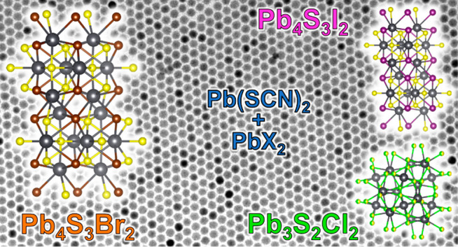
We report the colloidal synthesis of a series of surfactant-stabilized lead chalcohalide nanocrystals. Our work is mainly focused on Pb4S3Br2, a chalcohalide phase unknown to date that does not belong to the ambient-pressure PbS–PbBr2 phase diagram. The Pb4S3Br2 nanocrystals herein feature a remarkably narrow size distribution (with a size dispersion as low as 5%), a good size tunability (from 7 to ∼30 nm), an indirect bandgap, photoconductivity (responsivity = 4 ± 1 mA/W), and stability for months in air. A crystal structure is proposed for this new material by combining the information from 3D electron diffraction and electron tomography of a single nanocrystal, X-ray powder diffraction, and density functional theory calculations. Such a structure is closely related to that of the recently discovered high-pressure chalcohalide Pb4S3I2 phase, and indeed we were able to extend our synthesis scheme to Pb4S3I2 colloidal nanocrystals, whose structure matches the one that has been published for the bulk. Finally, we could also prepare nanocrystals of Pb3S2Cl2, which proved to be a structural analogue of the recently reported bulk Pb3Se2Br2 phase. It is remarkable that one high-pressure structure (for Pb4S3I2) and two metastable structures that had not yet been reported (for Pb4S3Br2 and Pb3S2Cl2) can be prepared on the nanoscale by wet-chemical approaches. This highlights the important role of colloidal chemistry in the discovery of new materials and motivates further exploration into metal chalcohalide nanocrystals.
Introduction
Over the past decade, lead chalcogenides first and lead-halide perovskites later have been among the cornerstone materials in nanocrystal (NC) research.1−3 Nowadays, many fundamental questions on these materials have been answered, and as interest in them is progressively shifting toward their applications, the quest for a new generation of inorganic NCs with appealing optoelectronic properties is becoming more compelling. An interesting class of compounds, which has hardly been explored on the nanoscale to date, is that of metal chalcohalides.4−7 These materials offer a rich solid-state chemistry8 and structural diversity,9,10 and they have proven to be useful for applications ranging from solar energy conversion to thermoelectrics, hard radiation detection, and superconductivity.11−14 Among them, lead chalcohalides have been investigated in the past, up to the complete determination of the atmospheric pressure PbY–PbX2 binary phase diagrams (Y = S, Se; X = Cl, Br, I),8 a search that led to the discovery and structural characterization of two stable (Pb5S2I6 and Pb7S2Br10) as well as some metastable chalcohalide structures (Pb4SCl6 and Pb4SeBr6).15,16 For the PbS–PbBr2 system, a few additional tentative stoichiometries have been identified.16−19 In various works, different compositions such as (PbBr)2S,17,18 “2PbS–PbCl2”, and “2PbS–PbBr2”16,19 have been reported and even partially characterized, with Rabenau et al. demonstrating that “2PbS–PbBr2” thermally decomposes into a mixture of Pb7S2Br10 and PbS.16 However, in the case of those latter phases the crystal structures were not determined, therefore precluding further investigations and leaving the door open to the possibility of identifying new lead chalcohalides. Indeed, Ni et al. recently synthesized in bulk two high-pressure phases, namely, Pb4S3I2 and Pb3Se2Br2, by means of a high-pressure solid-state reaction.20,21
In our attempt to synthesize colloidal lead sulfobromide NCs, we have discovered a phase that has not yet been reported, namely, Pb4S3Br2. We could prepare NCs of this material, which were roughly spherical in shape and had narrow size distributions, with an average size that was tunable from 7 to ∼30 nm. The NCs always exhibited an absorption onset at around 650 nm, which is compatible with the calculated bandgap of 1.98 eV (∼630 nm). We have been able to propose a structural model for this new material, based on single NC three-dimensional electron diffraction (3D-ED)22−25 and on X-ray powder diffraction (XRPD) data. Our findings were further supported by high-angle annular dark field scanning transmission electron microscopy (HAADF-STEM) tomography of an individual NC. Density functional theory (DFT) calculations confirmed an indirect bandgap, which explains the absence of an excitonic peak in the experimental optical absorption spectrum.
The structure we propose for the Pb4S3Br2 NCs shares close similarities with that of the recently published high-pressure (4 GPa) Pb4S3I2 phase,21 featuring the same space group and a comparable atomic layout. Differently from lead halide perovskites, and more akin to the case of lead chalcogenides, our Pb4S3Br2 NCs were colloidally stable in air and at room temperature for at least 2 months, a time span during which they did not undergo any structural, compositional, or optical changes. On the other hand, they thermally decomposed at temperatures above ∼250 °C, by forming a mixture of the thermodynamically stable PbS and Pb7S2Br10, which was consistent with what was already reported for other phases in the PbS–PbBr2 system.16 We also tested our Pb4S3Br2 NCs in photodetectors and solar cells, proving that these are indeed capable of both photoresponse and energy harvesting, even if with low efficiency in these initial attempts.
We could further extend our synthetic protocol to Pb4S3I2 and Pb3S2Cl2 NCs. The structure of the iodine-based NCs matches that of high-pressure bulk Pb4S3I2.21 The chloride-based NCs appear instead to be compatible with the stoichiometry and tentative X-ray pattern reported in 1969 by Rabenau et al. for a phase called “2PbS + PbCl2”, which, according to their report, they could neither purify nor fully characterize.16 Thanks to these clues, we discovered that the structure of our chlorine-based NCs closely resembles that of bulk Pb3Se2Br2, recently reported by Ni et al. as well,20 and we were able to adapt it in order to Rietveld fit our XRPD data.
We point out that none of these structures (Pb3S2Cl2, Pb4S3Br2, Pb4S3I2) belong to the ambient-pressure PbS–PbX2 phase diagrams.16 Hence, we find it remarkable that a colloidal chemistry approach has enabled us to prepare stable NCs of an entirely new group of metastable structures which in the bulk were obtained only under high-pressure conditions (Pb4S3I2) or in traces (Pb3S2Cl2) or that were never obtained at all to date (Pb4S3Br2).
Experimental Section
Chemicals
Lead thiocyanate (Pb(SCN)2, 99.5%), lead bromide (PbBr2, ≥98%), lead iodide (PbI2, 99%), lead chloride (PbCl2, 98%), oleylamine (OLAM, 70%), oleic acid (OA, 90%), 1-octadecene (ODE, 90%), NH4SCN (≥97.5%), Zn(CH3COO)2·2H2O (≥99%), Al(NO3)3·9H2O (≥98%), 1-ethyl-3-methylimidazolium iodide (EMII, 97%), methanol (MeOH, anhydrous, 99.8%), ethanol (≥99.5%), ethyl acetate (99.8%), and toluene (TOL, anhydrous, 99.8%) were purchased from Sigma-Aldrich. All chemicals were used without further purification (lead salts were stored under nitrogen).
Synthesis of Pb4S3Br2 NCs
All the syntheses of Pb4S3Br2 NCs were performed in air, without predrying chemicals or solvents, via a heat-up synthetic approach similar to the one developed by us for the synthesis of ultrathin PbS nanosheets.26 Briefly, 0.2 mmol of PbBr2 and 0.2 mmol of Pb(SCN)2 were dissolved in a mixture of 10 mL of ODE and 250 μL of OLAM and OA at 120 °C in a 25 mL three-necked flask. Then, the solution was quickly heated (∼20 °C/min) and started turning from light yellow to blood red above 150 °C, while the NCs nucleated and grew. The reaction was quenched by cooling the flask in a water bath; size control was achieved by varying the maximum temperature reached before quenching. Additionally, the NCs could be grown further by dropwise addition of a precursors solution over several hours at a constant temperature of 170 °C, as described in the discussion. Depending on their size, the NCs were recovered by simple centrifugation or by ethyl-acetate-assisted precipitation followed by centrifugation (6000 rpm for 5 min in both cases). Additional details on the synthesis are provided in the Supporting Information (SI, Section S.a).
Synthesis of Pb4S3I2 and Pb3S2Cl2 NCs
The Pb4S3I2 and Pb4S2Cl2 NCs were prepared by adapting the synthetic protocol developed for Pb4S3Br2. Simply, PbBr2 was replaced with an equimolar amount of the desired lead halide. For the synthesis of Pb4S3I2, since PbI2 was more soluble than PbBr2 in the reaction mixture, the synthesis could proceed as in the Pb4S3Br2 NC case without any further modification. However, a crystalline impurity, most likely PbI2 nanosheets or flakes, formed together with Pb4S3I2 NCs and could not be removed from the final product. For the synthesis of Pb3S2Cl2, as PbCl2 was less soluble than PbBr2 in the reaction mixture, longer times were needed for the solubilization (up to 1 h). We also performed a filtration with a 0.2 μm PTFE filter (Sartorius) to remove any undissolved residual before performing the heating step. The product was often contaminated by large-size PbS NCs, which could be removed by simple centrifugation, while the smaller Pb3S2Cl2 NCs remained suspended in the reaction batch and could be later recovered by ethyl acetate-assisted precipitation, as described for the Pb4S3Br2 NC case. Additional details on the syntheses are provided in the SI (Sections S.c,d).
Preliminary Characterization of the NCs
Absorption spectra from colloidal suspensions of NCs in toluene or hexane were recorded using a Cary300 spectrophotometer. The absence of any photoluminescence (PL) in the vis–IR region was probed using an Edinburgh FLS920 spectrofluorometer equipped with a Xe lamp and vis-PMT (up to 850 nm) and NIR-PMT detectors (liquid-N2-cooled housing, up to 1700 nm) by exciting at 400–450–500 nm. Low-magnification transmission electron microscopy (TEM) images were acquired on a JEOL JEM-1011 microscope equipped with a thermionic gun at an accelerating voltage of 100 kV. The samples were prepared by drop-casting diluted NC suspensions onto 200 mesh carbon-coated copper grids. HAADF-STEM images were acquired with a probe-corrected Thermo Fisher Scientific Titan microscope operating at 300 kV, with a semiconvergence angle of 20 mrad. Thermogravimetric analyses (TGA) were carried out on a TA Instruments TGA Q500 in an inert atmosphere (N2, 50 mL/min), first equilibrating the sample at 30 °C for 5 min and then heating at a constant rate of 10 °C/min up to 900 °C. Energy dispersive X-ray spectroscopy (EDX) was performed on a JEOL JSM-6490LA scanning electron microscope (SEM). The NCs were washed in ethyl acetate to remove the excess organics and unreacted precursors and drop-cast on a silicon wafer. TEM-EDX compositional analysis was performed on a Zeiss Libra TEM operating at 120 kV and equipped with a Bruker XFlash6T-60 detector.
3D Electron Diffraction Experiments on Individual NCs and Ab Initio Structure Solution
3D-ED22,23 data were collected on a Zeiss Libra TEM operating at 120 kV and equipped with a LaB6 source. Data acquisitions were performed in STEM mode after defocusing the beam to achieve a parallel illumination of the sample. A beam size of about 150 nm in diameter was obtained by inserting a 5 μm C2 condenser aperture. An extremely mild illumination was adopted to avoid any alteration or amorphization of the sample and to slow down the accumulation of organic contaminants. 3D-ED data were recorded with an ASI Timepix detector,27 which is able to register the arrival of single electrons and deliver a pattern that is virtually background-free. The camera length was 180 mm, with a theoretical resolution limit of 0.75 Å. 3D-ED data were taken from three roughly spherical NCs of ∼30 nm in diameter and four platelet-shaped NCs with lateral sizes of ∼30 × 80 nm. Both morphologies were found in the same synthetic batch (see details in the Results and Discussion section). 3D-ED data from the spherical NCs were collected with a stationary electron beam, while the sample was tilted in fixed steps of 1° for a total range up to 115°. Diffraction data acquired when the electron beam was precessed were blurred and therefore were not suitable for the 3D reconstruction. 3D-ED data from nanoplatelets were instead collected with a precessing beam obtained by a Nanomegas DIGISTAR P1000 device, while the sample was tilted in fixed steps of 1° for a total range up to 70°.28,29 The data were analyzed using ADT3D30 and PETS31 for cell and space group determination. The intensity integration for the structure determination was performed with PETS, using the standard integration and interpolation options. The ab initio structure solution was obtained using direct methods implemented in the software SIR2014.32 Data were treated within the kinematical approximation Ihkl ∝ Fhkl2.
Real-Space Atomic Resolution Electron Tomography of a Single NC
A tilt series of atomically resolved projection images was acquired on a single NC from −70° to +70°, with a tilt increment of 2°, using a Thermo Fisher Scientific Titan microscope operating at 300 kV with a semiconvergence angle of 20 mrad. To minimize the drift and compensate for scanning distortions during the acquisition, a series of images with a short dwell time was acquired at each tilt angle. Therefore, data restoration and registration were necessary before the tilt series could be aligned with respect to a common tilt axis. The first step in the calculation of the projection image was restoring the individual images of the time series by using a convolutional neural network.33 Next, these images were used as an input for a rigid and nonrigid average registration procedure.33 After an iterative alignment based on the phase correlation method, the tilt series was reconstructed using the simultaneous iterative reconstruction technique (SIRT) algorithm.34 The so-obtained reconstruction yielded atomic resolution data, which were converted into a 3D representation of the reciprocal space by calculating a Fourier transform (FT). From this 3D-FT, a 3D mask matching with the 3D-ED diffraction pattern corresponding to the NC was built, from which the unit cell parameters were extracted.
X-ray Powder Diffraction: Data Collection, Ab Initio Structure Solution, and Rietveld Refinement
XRPD analysis was performed in θ:2θ scan mode on a Panalytical Empyrean diffractometer, equipped with a 1.8 kW Cu Kα ceramic anode working at 45 kV–40 mA and a PIXcel3D detector. XRPD data were acquired on samples in the form of dry powders; the measurements were carried out in air at room temperature using a zero-diffraction silicon substrate. The ab initio structure solution by powder diffraction data was carried out using EXPO2014,35 a package able to perform all the necessary steps of the process, i.e., indexing, space group determination, full pattern decomposition, structure solution, and structure model optimization. Due to the broadening of peaks in the powder diffraction pattern, some of the above steps (i.e., indexing and space group determination) were carried out taking into account the information provided by 3D electron diffraction data. The indexing was performed using the software N-TREOR09,36 which is implemented in EXPO2014. The full pattern decomposition process in EXPO2014 alternates the application of the Le Bail algorithm to least-squares cycles that minimize the residual between the calculated and experimental profiles; the unit cell parameters belong to the set of refined variables. To reduce the errors on the integrated intensities estimates, a nondefault full pattern decomposition process was applied, exploiting the prior information on the positivity of the Patterson function. The integrated intensities were automatically supplied to direct methods (DM)37 to carry out the structure solution step, and an automatic procedure able to explore all the 20 stored DM sets of phases was executed, providing the corresponding 20 candidate structure models. Among them, the most plausible one, i.e., the one satisfying the main crystallochemical rules, was recognized by visual inspection via the user-friendly graphical tools of EXPO2014, allowing an easy check of the local chemical environment of the Pb atoms and of the crystal packing. Once the most reliable structural model had been identified and selected, it was further improved via the EXPO2014 graphic tools. Additional details concerning the ab initio structure solution steps by XRPD are provided in the SI (Section S.h).
Rietveld fits of the XRPD profiles were performed with the FULLPROF suite;38 the peak shape was described with a Thompson–Cox–Hastings pseudo-Voigt profile. The refined parameters were (according to the need of each fit): scale factor, multiple-point linear interpolation background, unit cell parameters, isotropic or anisotropic crystallite size (spherical harmonics), atomic coordinates, and thermal factors (isotropic normally, anisotropic if needed). The instrumental resolution function for the diffractometer was obtained by fitting the XRPD pattern of a LaB6 standard.39
Density Functional Theory Calculations
Band structure calculations were performed using the VASP package.40 The exchange–correlation potential was approximated by the PBE exchange–correlation functional,41 with the further inclusion of the spin–orbit coupling within the noncollinear approximation. We used a k mesh grid of 4 × 4 × 4 for the Brillouin zone integration. The atomic positions were relaxed until the forces were smaller than 0.001 hartree/angstrom. We used a kinetic energy cutoff of 400 eV.
3D Representation of Crystal Structures
All the visual representations of crystal structures in this work were created with the software EXPO2014,35 VESTA,42 or Mercury.43
X-ray and Ultraviolet Photoelectron Spectroscopy (XPS and UPS)
Samples for XPS and UPS investigations were prepared on Au-coated (50 nm) silicon substrates, by either drop-casting or following the same layer-by-layer method described later for the device fabrication (by spin-coating and solid ligand exchange procedures) in a N2-filled glovebox. Measurements were performed with a Kratos Axis Ultra DLD spectrometer. For XPS analysis, high-resolution spectra were acquired at a pass energy of 10 eV using a monochromatic Al Kα source (15 kV, 20 mA). The UPS measurements were performed using a He I (21.22 eV) discharge lamp, on an area of 55 μm in diameter, at a pass energy of 5 eV and with a dwell time of 100 ms. The work function (namely, the position of the Fermi level with respect to the vacuum level) was measured from the threshold energy for the emission of secondary electrons during He I excitation. A −9.0 V bias was applied to the sample to precisely determine the low-kinetic-energy cutoff, as discussed by Helander et al.44 Then, the position of the valence band maximum (VBM) versus the vacuum level was estimated by measuring its distance from the Fermi level.45
Fourier Transform Infrared Spectroscopy (FTIR)
We carried out attenuated total reflection–FTIR (ATR-FTIR) measurements under vacuum in a Bruker Vertex 70v on a 4000–550 cm–1 range and 100 repetition scans in order to evaluate the ligands present at the NC surface and their removal for the device fabrication. We performed the measurements by drop-casting 10 μL of NC colloidal suspensions directly on the diamond crystal. We analyzed both the suspension in toluene originally used for the devices preparation and that obtained from the redispersion in toluene of the scratched ligand-exchanged NC films (three layers, see also the following section on device preparation).
Photodetector and Solar Cell Fabrication and Characterization
The silicon/SiO2 (300 nm thermally grown, University Wafer) or the ITO/glass substrates (Ossila, 14–16 Ω/square) were first cleaned in an ultrasonic bath with acetone, followed by isopropanol (8 min each step), and finally dried by N2 flow. Then, N2 plasma treatment was carried out at 100 W for 2 min. The films (thickness ∼90 nm for the photodetectors, ∼160 nm for the solar cells, measured by a Veeco Dektak profilometer) were prepared via layer-by-layer deposition in four and seven consecutive steps, respectively. Each layer was deposited by spin-coating and ligand exchange procedures in a N2-filled glovebox. The removal of ligands from the surface of the NCs was evaluated by ATR-FTIR measurements. For each deposition step, the NC dispersion (50 mg/mL in toluene, filtered with a 0.2 μm PTFE Sartorius filter membrane) was spin-coated at 2500 rpm for 20 s (5 s ramp). Then, the substrate was dipped in a NH4SCN (1.2 mg/mL, for photodetectors) or a 1-ethyl-3-methylimidazolium iodide (EMII, 7 mg/mL, for solar cells) solution in MeOH for 20 s and rinsed by dipping in a beaker with MeOH before spin-coating again at 2500 rpm for 20 s for drying. To ensure the complete solvent evaporation, we stored the films in a N2-filled box overnight before carrying out the buffer layer or contact evaporation. For the solar cell, the buffer layer (MoO3, 12 nm, from Puratronic, 99.9995%, Alfa Aesar) and the Au top-metal contacts (80 nm, from EvoChem, 99.99%) were deposited onto the film by using a thermal evaporator inside a glovebox (rate 0.5 Å/s) with the help of a shadow mask (0.03 cm2 circular pads). The Al-doped zinc oxide (AZO) electron transporting layer was prepared in a two-step procedure by spin-coating at 2500 rpm for 30 s (5 s ramp) and subsequent annealing (140 °C for 10 min, 1 h ramp in a Nabertherm P330 furnace) of a precursor solution in ethanol. This step was carried out twice to reach a final AZO compact layer with a thickness of ∼50 nm. The precursor solution was prepared adapting an established protocol.46 Briefly, 1 g of Zn(CH3COO)2·2H2O and 18 mg of Al(NO3)3·9H2O were mixed in 8 mL of ethanol at 80 °C during 2.5 h and subsequently, still warm, filtered through a 0.2 μm PTFE filter membrane (Sartorius). The precursor solution was again filtered through a 0.2 μm PTFE filter membrane just before the spin-coating. For the photoconductor, the NC film was spin-coated onto a SiO2/Si substrate with prepatterned interdigitated electrodes (Ti/Au, 10/50 nm). The electrodes were prepared via standard photolithography and had an interelectrode gap of 1 μm.
SEM imaging of the films and devices was performed on a Helios Nanolab 600 DualBeam microscope (Thermo Fisher), using 5 kV and 0.2 nA as measurement parameters. Focused ion beam (FIB) was used to prepare cross-sections of the solar cell samples for evaluating the thickness of the layers forming the stack.
Photoconductivity Measurements
The photoelectrical characterization was performed in air, using a Keithley 2612 source meter connected to a KarlSuss–Microtech probe station in a two-probe configuration. As a light source, we used a mounted nine-array matrix of white-light-emitting diodes (LEDs, ILH-ON09-VA) from Intelligent LED Solutions with emission wavelength in the 400–750 nm range with a power density of 100 mW/cm2. Current–voltage and current–time (at fixed voltage) measurements were acquired during on/off light cycles.
Solar Cell Characterization
Current density–voltage (J–V) curves were recorded in air without device encapsulation using a Keithley 2400 source meter under 100 mW/cm2 (AM1.5G) illumination, provided by a LOT-Oriel LSH601/LSZ163 solar simulator. The light intensity was calibrated with a Newport 91150V reference cell. To test the shelf life, we stored the solar cells in the dark under ambient atmosphere.
Results and Discussion
Synthesis and Size Control of NCs
The Pb4S3Br2 NCs were prepared by modifying the heat-up synthetic approach described in our previous work on PbS nanosheets, which relies on the thermal decomposition of SCN– ions as a source of S2–, in the presence of Pb2+ and Br– ions.26 Our approach yielded nearly monodisperse polyhedral (roughly spherical) NCs, with an average diameter that was tunable between 7 and 16 nm. We were able to control the diameter by varying the maximum temperature reached before quenching the reaction (up to the limit of 190 °C). For example, quenching at 180 °C produced 14.2 ± 0.7 nm particles (Figure 1a and related inset). During the reaction, the originally formed nuclei grew as more and more S2– was released by the SCN– decomposition. The progress of the reaction could be tracked through monitoring any changes in the color of the solution or by examining the evolution of the absorption spectrum: the growth kinetics were explored by quenching several aliquots of the reaction batch at different temperatures and measuring the absorption spectra and particle size for each aliquot (Figure 1b, see also Figures S1–S4 and Table S1 of the SI). Heating above ∼190 °C caused the formation of a crystalline impurity, which contaminated the product. Based on the similarity of its XRPD pattern with that of PbI2 flakes (Figure S5) and on previous reports in the literature about the precipitation of PbBr2 in similar synthetic conditions,47 we suspect it is formed by a PbBr2 layered polymorph. Despite this, it was still possible to obtain larger particles and avoid the impurity precipitation, while also retaining a narrow size distribution, by further accreting a smaller batch of NCs at a lower temperature. Briefly, the crude reaction mixture of a synthesis quenched at 170 °C was reheated to the same constant temperature, and a PbBr2 + Pb(SCN)2 solution (prepared as in a standard heat-up synthesis) was added dropwise at a rate of 5 mL/h with a syringe pump. This enabled us to grow particles up to ∼30 nm in diameter (30 mL addition over 6 h, Figure S6), which were used for the 3D-ED experiments. As a side effect, NCs developed sharp facets, which were absent before the accretion process (Figure S6). Furthermore, nanoplatelets with essentially the same composition, as determined by EDX analysis, appeared as a side product, eventually becoming a consistent fraction (Figure S7 and Table S2). Most of them could be removed by decanting the reaction product in 40 mL of toluene and disposing the nanoplatelet-rich supernatant multiple times until the sample purity was satisfactory.
Figure 1.

Synthesis and characterization of Pb4S3Br2 NCs. (a) TEM image of Pb4S3Br2 NCs prepared by quenching the synthesis at 180 °C (Gaussian fit of their size distribution: 14.2 ± 0.7 nm, inset on the left). (b) Absorption spectrum of the sample reported in Figure 1a, along with a photograph of several aliquots of the same synthetic batch quenched at increasing temperatures (inset, T reported on labels in °C). As shown in Figure S3, the spectral profile is not dependent on the particle size, and the color difference depends only on the concentration increment. (c) XRPD pattern of Pb4S3Br2 NCs compared with that of PbS (ICSD-38293) and Pb7S2Br10 (ICSD-21041), evidencing that there is no match with these most obvious candidates.
Compositional and Structural Characterization
We first determined the stoichiometry of our NCs via XPS, which yielded an atomic elemental ratio of Pb:S:Br = 43:32:25. This was consistent with the proposed Pb4S3Br2 stoichiometry (Pb:S:Br = 44.4:33.4:22.4) after the instrumental errors and crystal termination effects had been considered (Figure S8 and Table S3). A similar stoichiometry was also measured on a film of NCs via SEM-EDX analysis (Pb:S:Br = 43:30:27, see Figure S9a,b and Table S4). We also verified that Pb, S, and Br were uniformly distributed in the NCs through STEM-EDX analysis (Figure S9c–f). Until now, no compound with such a stoichiometry has been reported, and the XRPD pattern could not be assigned to any known structure (Figure 1c): this was the first hint that we had obtained a new crystalline phase. To gain a better insight into the stoichiometry of this new material, we investigated our NCs by a combination of thermogravimetry and XRPD analyses. A sample that had been washed with ethyl acetate to remove the excess of ligands and unreacted precursors was decomposed in an N2 atmosphere on a 10 °C/min thermal ramp up to 900 °C, evidencing three mass losses at around 250, 500, and 800 °C (Figure 2a).
Figure 2.
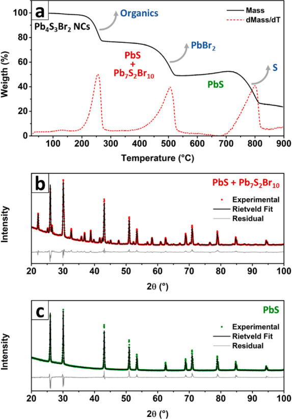
Thermal stability and decomposition of Pb4S3Br2 NCs. (a) TGA curve of a Pb4S3Br2 NC sample, showing the three distinct weight losses that the material undergoes upon heating. (b) Rietveld fit of the product of the first mass loss (∼350 °C), demonstrating that what is left after this step is a mixture of PbS and Pb7S2Br10. (c) Rietveld fit of the XRPD pattern for the product of the second mass loss (∼600 °C), demonstrating that only PbS is left.
XRPD patterns were acquired before the analysis and after the first two mass loss steps, demonstrating that the sample first decomposed to a mixture of Pb7S2Br10 and PbS (Figure 2b), then further degraded to pure PbS (Figure 2c). The first step was found to be heavily sample-dependent in terms of mass loss and occurred in a temperature range (up to ∼250 °C in Figure 2a) that was compatible with the desorption of organic molecules (solvent and ligands, see SI Section S.d).48 Concomitantly with this organic mass loss, the inorganic fraction recrystallized into a mixture of Pb7S2Br10 and PbS. The second mass loss (up to 500 °C), instead, occurred due to the loss of PbBr2, which is known to be a rather volatile compound in its molecular form.49,50 This is consistent with the fact that the only product left after the second mass loss was PbS. Hence, in this second step, the following decomposition reaction took place:
We exploited the results from TGA and XRPD to calculate the initial composition of our material and obtained atomic elemental ratios for Pb:S:Br equal to 44.5:33.5:22.1 (based on four TGA analyses on four different NC samples, see Table S5). These ratios are in excellent agreement with the XPS measurements and with the proposed Pb4S3Br2 stoichiometry (see Figures S10–S12 and Table S5 for details). Finally, the third mass loss (Figure 2a) is compatible with the decomposition of PbS and sublimation of S.51
Before proceeding with the collection of structural data (summarized in Figure 3), we inspected some individual NCs via HAADF-STEM imaging (Figure 4a). The NCs proved to be single-crystalline and homogeneous, with no evident differences between the core and the surface regions. Neither the STEM images nor their corresponding FTs could be matched with known phases, reinforcing the idea that our NCs had a structure that was unknown to date. During the analysis, some degree of electron beam damage was observed upon scanning: the outer surface of the NCs amorphized. Furthermore, several high-contrast crystalline particles (∼5 nm), which were identified as Pb and PbS, based on their crystal structure, were formed (Figure S13). The nucleation and growth of metallic Pb clusters upon beam-induced halide sublimation is not surprising, as it has been observed before when investigating lead halide perovskite NCs.52,53 On the other hand, the presence of PbS is consistent with our observations on the decomposition of this metastable material through the TGA-XRPD analysis discussed earlier.
Figure 3.

3D-ED and 3D-FT on Pb4S3Br2 NCs. (a) TEM image of the large faceted Pb4S3Br2 NCs obtained via the accretion process described in the discussion and investigated via 3D-ED and (b–d) 3D ED reciprocal space of a NC oriented along the main reciprocal directions. (e) 3D electron tomography reconstruction of one spherical Pb4S3Br2 NC and (f–h) the corresponding 3D-FT projected along the main reciprocal directions (before application of the mask, see details in the text).
Figure 4.

HAADF-STEM and 3D-FT of Pb4S3Br2 NCs; 3D-ED and XRPD structural models for Pb4S3Br2. (a) Atomic resolution images of Pb4S3Br2 NCs evidencing their single-crystalline nature. Insets: Corresponding FT. (b) Two projections of the calculated 3D-FT, oriented so that the reciprocal cell base vectors are clearly recognizable. (c) The models obtained from 3D-ED and from XRPD converge to the same structure upon DFT relaxation. (d) Pb4S3Br2 NC crystal structure as obtained at the end of the workflow described in the main text, together with (e) the coordination polyhedra for the three nonequivalent lead crystallographic sites. (f) Rietveld refinement of the XRPD pattern based on the structure shown in panel d.
In order to gain insight on this new crystal structure, we performed 3D-ED experiments on the largest polyhedral NCs that we could synthesize (∼30 nm, Figure 3a–d). We identified an orthorhombic cell with parameters a = 8.2(2) Å, b = 14.6(3) Å, c = 8.1(2) Å. Unfortunately, our experimental setup cannot collect precession data from NCs smaller than 50 nm; therefore we could not directly acquire robust information about the symmetry and the atomic positions.54 Precession 3D-ED data could instead be obtained from the nanoplatelets (Figure S14) that were found as byproducts in the same batch, and these delivered slightly different cell parameters, a = 8.0(2) Å, b = 15.5(3) Å, c = 7.9(2) Å. The crystallographic c axis was found to be always parallel to the main direction of growth of the platelets, while the b axis was orthogonal to the main platelet facet. The space group was unambiguously determined as Pnma (#62) via systematic extinction analysis, and the structure could be reliably solved ab initio on the basis of 3D-ED data (Table S6). Assuming the same space group for the spherical NCs, a tentative yet comparable ab initio structure was also obtained with nonprecessed data collected from the spherical NCs, suggesting a very close structural resemblance between the two types of NC morphologies (namely, the roughly spherical NCs and the nanoplatelets, Figure S15). Consequently, we assumed as a first description of the NC structure a hybrid cell, featuring the unit cell parameters of the spherical NC and the atomic coordinates of the nanoplatelets.
In the attempt to confirm the structural model obtained from the 3D-ED data, we acquired the direct-space atomic resolution 3D tomography of a single ∼16 nm spherical NC. Upon the acquisition of the first HAADF-STEM images, we again observed immediate electron beam damage and amorphization at the outer atomic layers of the NC. However, during the rest of the experiment the damage did not progress further, and consequently the inner part of the 3D reconstruction could be used for further analyses (Figures 3e and S16, Movie_S1). We did not succeed in extracting the atomic coordinates from the tomography data, due to the high structural complexity and most likely also due to the beam damage. However, we could compute its 3D-Fourier transform (3D-FT, Figure 3b), which produced a 3D map of the NC reciprocal space, which is comparable to that obtained by 3D-ED (Figure 3f–h). The data were cleaned from noise and interferences by applying a mask built on the base of the proposed unit cell (Figures 4b and S17, Movies_S2 and S3), which correctly fitted the data and allowed us to extract an orthorhombic cell with lattice parameters a = 8.3 Å, b = 15.1 Å, c = 8.2 Å, in close agreement with that from the 3D-ED.
Hence, by combining data from 3D-ED and 3D-FT we could confirm the unit cell of the spherical NCs. In order to check the atomic coordinates as well, we attempted an independent ab initio structure solution from XRPD using the software EXPO2014.35 The first and most critical step of the XRPD-based structural solution, especially in the case of nanomaterials, is the indexing process. The broad and largely overlapped peaks characteristic of NC XRPD prevented the indexing procedure from identifying the cell parameters with high confidence and by a default run (see SI).55 For the same reason, the automatic space group determination failed due to the unavoidable errors on the integrated intensities. The selection of the unit cell was therefore guided by the information provided by the analysis of 3D-ED, and the space group Pnma was considered for carrying out the ab initio structure solution. At the end of the solution process, the structural model determined on NCs by XRPD (Figure S18 and Table S7) was found to be very similar to the one determined by 3D-ED. The two structures are characterized by a root-mean-square deviation (RMSD) equal to 0.534 Å, where RMSD = sqrt(∑idi2/Nau), i.e., the square root of the averaged squared distances between couples of corresponding atoms in the two compared models, with Nau the number of atoms in the asymmetric unit (Figure S19). The unit cell parameters refined from XRPD by EXPO2014 (a = 8.22592 Å, b = 14.70843 Å, c = 8.13988 Å) were in good agreement with the ones of the 3D-ED procedure as well. In order to further confirm the equivalence of the models obtained independently by 3D-ED and XRPD, we relied on DFT calculations to relax both structures, by minimizing the interatomic forces. We kept the cell parameters fixed to the more precise values extracted from the XRPD data. The two structures relaxed to the same model: this confirmed that they are equivalent, and, since they came from independent data sets and techniques, we consider this agreement a good proof of their reliability (Figure 4c, see also Figure S20). It is also worth noting that the 3D-ED-derived model was the one closer to the relaxed structure.
The structure we propose for Pb4S3Br2 at the end of this multiple-technique workflow (Figure 4d,e, see also Figure S21) is orthorhombic; it belongs to the Pnma (#62) space group and has unit cell parameters a = 8.226 Å, b = 14.708 Å, c = 8.140 Å. Lead atoms are involved in three different coordination environments. Every lead atom is octacoordinated, with two Pb sites surrounded by 4 S + 4 Br and one Pb site surrounded by 6 S + 2 Br. Sulfur is found in two nonequivalent crystallographic sites, both with a distorted octahedral coordination (as found in PbS), while bromine occupies a heptacoordinated pentagonal bipyramidal site. We want to point out that the unit cell parameters were independently confirmed by three different techniques (3D-ED, XRPD, atomic resolution electron tomography) and are most likely correct. The Rietveld refinement of the structure based on the XRPD pattern confirmed the values (a = 8.202 Å, b = 14.707 Å, c = 8.165 Å, Figure 4f, Figure S22 and Table S8) and had a minor impact on the atomic coordinates, which were almost unchanged as well. The residual curve however highlights some minor discrepancies, probably arising from a combination of factors, such as the struggle of the Rietveld method to correctly fit the many broad overlapping reflections and the presence of strain or distortions.
There are striking similarities between the Pb4S3Br2 phase we propose for our NCs and the recently discovered Pb4S3I2, which was obtained at high pressures and temperatures (4 GPa, 600 °C) in the form of bulk crystals.21 Both phases have the same Pb4S3X2 stoichiometry, crystallize in the same space group, and have an equivalent atomic layout (Figure S21). For example, in both structures the Pb atoms form layers along the b axis, while the anions are alternated in sulfur-only and mixed sulfur–bromine layers.18 This evidence confirms that we have discovered a structural variation in a yet underexplored family of compounds: our hypothesis is that Pb4S3Br2 is a kinetically trapped high-pressure metastable structure as well. First, the reader should be reminded that the room-pressure pseudobinary phase diagram PbS–PbBr2 contemplates only PbS, PbBr2, and Pb7S2Br10 as stable phases.16 This is consistent with what we observed in our TGA-XRPD experiments: thermally annealing the NCs at temperatures above 250 °C causes their transition into a mixture of the thermodynamically stable PbS and Pb7S2Br10 phases. Second, if compared to the published Pb4S3I2 model, the Pb4S3Br2 structure appears to be contracted along the b axis (−5.5%), while the a and c axes retain basically the same length (a = +1.2; c = −0.5%), suggesting some sort of anisotropic structural relaxation. Furthermore, the hypothesis of Pb4S3Br2 being itself a metastable high-pressure phase is consistent with the morphology-dependent structural relaxation that we observed in our samples.
We discussed above that NCs and nanoplatelets feature closely related structures, distinguished only by the length of the b parameter and by a minor rearrangement of the atomic positions. To gain insight on this peculiar behavior, we again relaxed our 3D-ED and XRPD structural models by DFT calculations, this time letting the unit cell parameters a, b, and c to vary. Remarkably, both models converged to a structure that was close to that obtained ab initio from 3D-ED data for the nanoplatelets, especially in terms of unit cell parameters (3D-ED a = 8.0 Å, b = 15.5 Å, c = 7.9 Å; DFT a = 8.14 Å, b = 15.42 Å, c = 8.08 Å, Figure S20). This suggests that the latter represents the relaxed form of the otherwise kinetically trapped high-pressure phase found in the spherical NCs. It is worth noting that the b axis, which is the one varying the most from nanoplatelets to NCs, is perpendicular to the nanoplatelet surface, a possible indication that the relaxation prevents the accretion of the crystal in the relaxed direction, while at the same time allowing the lateral growth (along the a and c directions). The different cell parameters observed for the two nanoparticle morphologies and the impossibility of growing pseudospherical NCs larger than ∼30 nm in diameter suggest a critical size transition in cell parameters. We hypothesize therefore that a sort of high-pressure phase is possible only for the smaller NCs, most likely as a result of an overall energy balance in which the surface energy term plays an important role.
Optoelectronic Properties
Pb4S3Br2 NCs feature a strong absorption in the visible, starting from an intermediate region between that of the white wide-bandgap lead bromide (∼4 eV in bulk)56 and of the black small-bandgap lead sulfide (0.59 eV for 10 nm NCs, 0.41 eV in bulk).57,58 The absorption decreases toward lower energies and becomes negligible after ∼650 nm (1.91 eV), causing the material to appear red in a concentrated solution (Figure 1b). Interestingly, we observed that the absorption spectrum remains unchanged while varying the size of NCs in our tunability range (7–16 nm), thus suggesting that quantum confinement effects are negligible for Pb4S3Br2 (Figure S3). Also, no photoluminescence was detected in the range 500–1700 nm. The observed spectral features are consistent with the ones predicted by computing the band structure: calculations were performed at the DFT/PBE level of theory, which included spin–orbit coupling (SOC), on both the cell-relaxed and the cell-fixed structures (respectively corresponding to the spherical Pb4S3Br2 NCs and nanoplatelets). Noteworthily, the results of the simulations do not change drastically, as in both cases an indirect bandgap of ∼1.5 eV is predicted (Figure 5a, see also Figure S23). However, the PBE functional is known to underestimate the bandgap for extended systems, due to a strongly localized hole.59 In this case, the spin-free bandgap value for lead sulfide systems is a better approximation to the experimental bandgap as a consequence of error cancellation.60 For comparison, we thus computed the bandgap without SOC (Figure S23), which lies at 1.98 eV, closer to the absorption onset of 1.91 eV (650 nm) estimated from the experimental spectrum. The density of states calculation highlights that the two elements, Pb and S, mainly contribute to the band-edge states, while the Br-related states are mainly located deeper below the valence band edge (Figure 5b).
Figure 5.
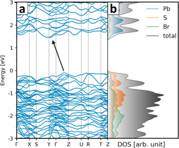
Pb4S3Br2 NCs’ band structure. The band structure was calculated at the DFT/PBE+SOC level of theory on the model shown in Figure 4d. The band structure features an indirect bandgap. The density of states diagram shows that the elements mostly contributing to the band-edge states are S for the valence and Pb for the conduction band, while Br-related states fall deeper in the valence band.
Stability, Ligand Exchange, and Testing of Pb4S3Br2 NCs in Devices
The electronic structure of this material, together with its chemical affinity with the optically active lead-bromide perovskites and lead chalcogenides, suggests a potential exploitation of Pb4S3Br2 NCs as an active layer in photosensitive devices. In the perspective of applications, we performed basic temporal stability tests. NCs were stored at room temperature in the dark both as a diluted colloidal suspension in toluene and as a dry powder. The absorption spectra and XRPD patterns were compared with that of the fresh samples after two months, and no difference was found (Figure S24). Encouraged by these results, we fabricated both photodetector and solar cell test devices. The Pb4S3Br2 NCs for the devices fabrication were prepared by quenching the reaction at 170 °C, centrifuging at 6000 rpm for 5 min, discarding the precipitate, and then recovering the NCs in the supernatant via ethyl-acetate-assisted precipitation, which also partially washed the excess of organics from the synthesis.
Prior to the device fabrication, we tested two ligand exchange procedures directly on NC films, in order to replace the long molecules on the NC surface with shorter ligands and thus improve the film conductivity (additional details can be found in the Experimental Section). In the FTIR spectrum of the as-prepared NCs (Figure S25, top spectrum) one can observe main bands located at 2953/2924/2853 cm–1 together with features at 1466/1412 cm–1, which corresponds respectively to the CH3 and CH2 stretching and CH2 bending of the alkyl chains from oleic acid and/or oleylamine.26,61 Moreover, the appearance of a band at 1520 cm–1 corresponding to the C=O stretching confirms the presence of Pb-bound oleate at the NC surface.61 A broad band at 2040 cm–1 (S=C=N stretching) and features at 1312/1266 cm–1 (C–N stretching), which can be attributed to SCN– and to oleylamine attached at the NC surface, respectively, were present as well.26,62 Hence, we concluded that the surface passivation of the as-synthesized NCs comprises various ligand molecules. However, after ligand exchange using NH4SCN or EMII all the long-chain ligands coming from the synthesis were removed, as indicated by the disappearance of the corresponding FTIR bands (Figure S25, middle and bottom spectra) and confirmed by XPS analysis, where the peaks related to carbon and oxygen were absent after the exchange (Figure S26, see also Figures S27 and S28 for UPS analyses).
We tested the response of Pb4S3Br2 NCs in a photoconductor device fabricated by layer-by-layer spin-coating the NC dispersion onto Si/SiO2 substrates with prepatterned interdigitated electrodes (Figure 6a,b). The layer-by-layer deposition, followed by ligand exchange with thiocyanate (using NH4SCN as a SCN– source), was repeated four times to produce a compact film (thickness ∼90 nm, Figure 6a). When measured in the dark, the devices produced low current (<pA at 20 V). Then, under white light (400–750 nm, 100 mW/cm2), the device immediately responded, with a current of ∼10 nA, as shown in Figure 6c.
Figure 6.

Pb4S3Br2 NCs photoconductor and solar cell characterization. (a) Section of the Pb4S3Br2 NC film on a photodetector (SEM). (b) Optical microscope image of the photodetector with interdigitated electrodes. (c) Current response during light on/light off cycles of a device with interdigitated electrodes. (d) SEM image of a solar cell stack cross-section. (e) Energy level alignment in the stack (Pb4S3Br2 values measured by UPS; ITO, AZO, MoOx, and Au values from the literature, see refs (46), (68)–71, respectively). (f) Current–voltage curve under AM1.5G illumination for a solar cell with the stack shown in panel c. Inset: Photo of a representative sample.
The responsivity R = Iphoto/Popt (Iphoto = photocurrent, Popt = optical power on the device) was measured on four different devices to be R = 4 ± 1 mA/W (best device 5 mA/W), The detectivity was (3 ± 1) × 108 Jones, estimated from the noise power density spectrum of a time trace acquired in the dark (Figure S29).63 We also evaluated the normalized photocurrent to dark current ratio NPDR = R/Idark (Idark = dark current), a suitable figure of merit in the case of devices with very low dark current.64 In our case, we measured NPDR = (8.5 ± 2.8) × 105 mW–1. For the solar cell tests, we prepared a layered stack on an ITO/glass substrate comprising AZO (as electron transport layer, ETL), the photoactive Pb4S3Br2 NCs layer, MoOx as a buffer layer, and Au as top contact (Figure 6d). In order to make the Pb4S3Br2 NCs layer conductive, a ligand exchange was performed with iodine (using EMII as a I– source), as described earlier. The suitability of the energy level alignment resulting from the ligand exchange in the layered stack was verified by UPS measurements (Figure 6e, see also SI Section S.o for details regarding XPS and UPS analyses). With this configuration, the nonencapsulated best solar cell showed a PCE of 0.21 ± 0.02% (average from four different devices), Jsc = 1.2 mA cm–2 (1.09 ± 0.07 mA/cm2), and Voc= 0.57 V (0.58 ± 0.03 V) under a standard AM1.5G illumination in air (Figure 6f). The solar cells demonstrated a good long-term stability under ambient atmosphere, retaining 60% of the PCE after more than 2 months of storage (Figure S30). The performance showed by our devices (R = 4 ± 1 mA/W or PCE = 0.21%), in comparison with state-of-the-art for NC-based devices, is not reaching the common figures of merit of responsivity or PCE. Responsivity in photoconductors built with lead halide perovskites exceeds 106 A/W, and even early results with CdX (X = S, Se, Te) reached 200 mA/W (see, for example, refs (65)–67).
We compared the NPDR of our photodetectors with that of metal/semiconductor/metal devices and found that our system performs well in comparison, for example, with semiconductor/CNT72 or semiconductor/graphene73 systems, typically featuring values of ∼104 mW–1, or nanostructured silicon74 (∼104 mW–1) and is comparable with nanomembrane-enhanced Ge detectors;75 our configuration offers nonetheless a simpler fabrication protocol. We could reach these results thanks to the very low dark current, which also suggests that these devices can operate with low power consumption. Instead, regarding the performance of the solar cell and comparing it with systems absorbing in the visible range, the PCE obtained is far from the results achieved with CsPbI3 (13.4%)76 or CdTe quantum dots (11.6%).77 Considering the results from the photoconductor and solar cell, we could envision for our material a role in multilayer stacks operating as a charge transport layer with some additional photogeneration62,63 rather than as the main active layer, whose band alignment can be favorably tuned by surface chemistry (SI Section S.o). Indeed, our material reaches a responsivity comparable to the ones of polymers (0.2–0.7 mA/W),54 which are commonly used as charge transport layers.
Preliminary Investigation of Iodide and Chloride-Based NCs
Driven by the strong analogy between the structure of our NCs and that of the reported high-pressure phase Pb4S3I2, we tried to prepare NCs of other chalcohalides by using PbI2 and PCl2 in place of PbBr2 as halide precursors in the synthesis: in both attempts we obtained colloidal nanoparticles. In the case of Pb4S3I2, the NCs were larger than for the Pb4S3Br2 case discussed above (up to hundreds of nm and polydisperse) and had the shape of elongated prisms or rods (Figure 7a, see also Figure S31). The color was slightly different from that of Pb4S3Br2, tending to brown, most probably due to the scattering caused by the large size of obtained NCs. We confirmed the crystal structure by Rietveld fitting the XRPD pattern on the base of the structure published by Ni et al.,21 discovering at the same time the presence of a byproduct identified by some residual peaks, which we suspect to be PbI2 nanosheets or flakes on the basis of the match with published XRPD data (Figure S32 and Table S9).78,79 We take the remarkable resemblances between the XRPD patterns of Pb4S3I2 and Pb4S3Br2 as an additional proof of the close similarity of the two structures.
Figure 7.

Characterization of Pb4S3I2 and Pb3S2Cl2 NCs. TEM images of (a) Pb4S3I2 and (b) Pb3S2Cl2 NCs. (c) XRPD patterns of the three NC samples (Pb4S3I2, Pb4S3Br2, Pb3S2Cl2) and related Rietveld fits (Tables S3, S4, and S9). The red asterisks in the Pb4S3I2 pattern highlight the peaks coming from an impurity, most likely PbI2 nanosheets or flakes. (d) Optical absorption spectra of the three samples. The almost perfect overlap suggests that, despite the different composition, stoichiometry, and structure, the halides play a very minor role in the optical properties of this class of nanomaterials. The only appreciable trend is visible at the onset of the spectrum (inset).
The chlorine-based NCs we prepared were instead smaller than the Pb4S3Br2 NCs prepared under comparable conditions (7.0 ± 0.8 nm when quenched at 170 °C), but they featured a very similar shape (roughly spherical, Figure 7b and Figure S33a). The synthesis often produced PbS NCs as a byproduct, which could however be removed by simple centrifugation due to their larger size (see Figure S33b). The color of the purified product was almost identical to that of Pb4S3Br2 NCs. Thus, we were surprised to discover that the XRPD pattern of the two phases, namely, the Cl-based NCs (Figure 7c, green pattern) and the Pb4S3Br2 NCs (Figure 7c, blue pattern) were remarkably different. A close match with the XRPD lines reported in 1969 by Rabenau et al. for the tentative “2PbS + PbCl2” phase first made us suspect that we had obtained the same compound.16 By XPS compositional analysis we measured Pb:S:Cl ratios corresponding to 42.5:23.9:33.6, which are consistent with the proposed Pb3S2Cl2 stoichiometry (Pb:S:Cl = 42.9:28.6:28.6) if measurement errors and crystal termination effects are considered. Driven by this finding, we searched the literature for comparable structures and found that Ni et al. recently reported the bulk synthesis (4 GPa, 700 °C) and complete structural characterization of the high-pressure phase Pb3Se2Br2.20 Given the resemblances of stoichiometries and XRPD patterns, our hypothesis was that we had found an isostructural compound: to confirm it, we Rietveld fitted the XRPD pattern of Pb3S2Cl2 NC with a model adapted from that published by Ni et al. by replacing Se with S and Br with Cl, and we found a good match (Figure S34 and Table S10). The slight misplacement of the peaks is probably due to a slight deformation of the originally cubic unit cell, but the excessive broadening of the reflections due to the small size of NCs prevented us from gaining a better insight of the material structure. We plan to investigate this aspect in further, more focused studies. We found it remarkable that atoms in Pb3S2Cl2 show the same coordination environment found in the other two isostructural materials we reported (Pb = octacoordinated, Cl, S = deformed octahedral), suggesting that the structural variety in this class of lead chalcohalides may arise mainly from a different arrangement of the fundamental structural units (Figure S21).
Surprisingly, despite the major compositional and structural differences among the three stoichiometries, their absorption spectra are almost identical (Figure 7d). The only appreciable trend regards the onset of the spectra, which exhibit a weak red-shift on going from the chloride to the bromide and then to the iodide-based NCs, suggesting a slightly variable bandgap. Another key element to understand the electronic properties of this class of materials is, as we already mentioned, the absence of size dependency in the optical spectra of Pb4S3Br2 NCs. The same is likely true also for Pb4S3I2 and Pb3S2Cl2, as the remarkable overlap of the three spectra would be an astonishing coincidence otherwise. Finally, we observed that the contribution of the halide to the band-edge states of Pb4S3Br2 is negligible (Figure 5b). A very similar trend was predicted, through DFT calculations, also for Pb4S3I2 and Pb3S2Cl2 (Figure S35). The calculations additionally confirmed the halide-dependent shift of the bandgap (Pb3S2Cl2 = 2.02 eV, Pb4S3Br2 = 1.98 eV, Pb4S3I2 = 1.76 eV), indirect for all of them, which is in good agreement with the experiments. Considering all these observations, our conclusion is that the optical properties of these materials are probably dominated by localized Pb–S interactions. The main effect of the halides is to cause this localization: PbS has an exciton Bohr radius of 18 nm, and most of our NCs are well below this size threshold.80,81 The mild, halide-dependent shift in the absorption onset is probably due to the local alteration of the electron density surrounding the lead atoms.
As a note, we want to highlight that the formation of these lead chalcohalide phases must be taken into account when performing the synthesis of PbS NCs, as they often exploit lead halide salts as precursors and are normally conducted under conditions similar to what we reported.82,83 Furthermore, recent work has demonstrated that PbS NCs synthesized from PbCl2 have a PbCl2-rich surface, leading to improved photoluminescence quantum yield and chemical stability, which might be related to the passivation by a layer of the hereby reported Pb3S2Cl2 phase.84−86 This hypothesis may stimulate further studies aiming at a more detailed characterization of those systems.
Conclusions
In conclusion, we have reported the synthesis of colloidal NCs of a previously unknown, metastable phase belonging to the PbS–PbBr2 system, namely, Pb4S3Br2. Our synthetic protocol delivers NCs with a narrow size distribution and size tunability over the range 7 to ∼30 nm. We were able to solve its structure by a combination of 3D electron diffraction, high-resolution HAADF-STEM tomography, and powder XRD diffraction, demonstrating that Pb4S3Br2 is a metastable structural analogue of the recently reported high-pressure Pb4S3I2 phase. Our material is an indirect 1.98 eV bandgap semiconductor and exhibits photoresponse and photoharvesting capabilities, which were tested in a photodetector and a solar cell. Finally, we applied the same synthetic protocol to prepare NCs of the high-pressure Pb4S3I2 phase and of a new Pb3S3Cl2 chalcohalide phase. Both are indirect bandgap semiconductors (1.76 and 2.02 eV, respectively). We expect that the discovery of these new lead chalcohalide NCs will encourage the exploration of other metal chalcohalides, a group of materials that to date has been vastly untapped at the nanoscale.
Acknowledgments
We would like to thank Dr. A. Toma for the access to the IIT clean room facilities’ SEM/FIB and evaporators, the Smart Materials group (IIT) for the access to the ATR-FTIR equipment, S. Marras for the support during XRPD measurements, G. Pugliese for help with the TGA measurements, M. Campolucci for help with the experiments on NC growth kinetics, S. Lauciello for help with the SEM-EDX analyses, and D. Baranov and R. Brescia for the helpful discussions. We also acknowledge funding from the Programme for Research and Innovation Horizon 2020 (2014–2020) under the Marie Skłodowska-Curie Grant Agreement COMPASS No. 691185. I.I. acknowledges the Dutch NWO for financial support under the Vidi scheme (Grant No. 723.013.002). S.B. acknowledges support by means of the ERC Consolidator Grant No. 815128 REALNANO. E.M. and M.G acknowledge the Regione Toscana for funding the purchase of the Timepix detector through the FELIX project (Por CREO FESR 2014–2020 action).
Supporting Information Available
The Supporting Information is available free of charge at https://pubs.acs.org/doi/10.1021/jacs.0c03577.
Crystal structure of Pb4S3Br2 NCs as obtained from 3D-ED/XRPD + DFT relaxation (CIF)
Crystal structure of Pb4S3Br2 NCs as obtained after Rietveld refinement (CIF)
Crystal structure of Pb3S2Cl2 (adapted from the published Pb3Se2Br2) after Rietveld fit (CIF)
Experimental procedures for the synthesis of Pb4S3Br2, Pb4S3I2, and Pb3S2Cl2 NCs; XPS, EDX, TGA, UPS, FTIR, HAADF-STEM analyses on Pb4S3Br2 NCs; 3D electron tomography and 3F-FT of Pb4S3Br2 NCs; 3D-ED and XRPD-based structure solution for Pb4S3Br2 NCs; proposed crystal structures for Pb4S3Br2, Pb4S3I2, and Pb3S2Cl2 NCs; Rietveld fits of Pb4S3Br2, Pb4S3I2, and Pb4S3Cl2 NC XRPD patterns; DFT relaxation of Pb4S3Br2 NC structural models; DFT calculations of Pb4S3Br2, Pb4S3I2, and Pb3S2Cl2 NC band structures; temporal stability tests on Pb4S3Br2 NCs; complementary characterization for Pb4S3Br2 NC-based devices (PDF)
Graphical representations of the 3D electron tomography of one Pb4S3Br2 NC (AVI)
Graphical representation of Pb4S3Br2 NC’s computed 3D-FT before the application of a 3D-ED-based mask (AVI)
Graphical representation of Pb4S3Br2 NC’s computed 3D-FT after the application of a 3D-ED-based mask (AVI)
Author Present Address
▽ Department of Chemistry and Applied Biosciences, ETH Zürich, Vladimir Prelog Weg 1, CH-8093 Zürich, Switzerland.
Author Present Address
⬡ CIC nanoGUNE, Tolosa Hiribidea, 76, E-20018 Donostia, San Sebastian, Spain.
Author Present Address
△ IHP–Leibniz-Institut für Innovative Mikroelektronik, Material Research Semiconductor Optoelectronics, Frankfurt (Oder), Germany.
Author Present Address
○ School of Materials, Sun Yat-sen University, Guangzhou, 510275, China.
Author Contributions
▲ S. Toso, Q. A. Akkerman, and B. Martín-García contributed equally.
The authors declare no competing financial interest.
Supplementary Material
References
- Akkerman Q. A.; Rainò G.; Kovalenko M. V.; Manna L. Genesis, Challenges and Opportunities for Colloidal Lead Halide Perovskite Nanocrystals. Nat. Mater. 2018, 17 (5), 394–405. 10.1038/s41563-018-0018-4. [DOI] [PubMed] [Google Scholar]
- Lu H.; Carroll G. M.; Neale N. R.; Beard M. C.. Infrared Quantum Dots: Progress, Challenges, and Opportunities. ACS Nano; 2019, 939–953, 10.1021/acsnano.8b09815. [DOI] [PubMed] [Google Scholar]
- Mcdonald S. A.; Konstantatos G.; Zhang S.; Cyr P. W.; Klem E. J. D.; Levina L.; Sargent E. H. Solution-Processed PbS Quantum Dot Infrared Photodetectors and Photovoltaics. Nat. Mater. 2005, 4 (2), 138–142. 10.1038/nmat1299. [DOI] [PubMed] [Google Scholar]
- Mihailovic D.Inorganic Molecular Wires: Physical and Functional Properties of Transition Metal Chalco-Halide Polymers. Progress in Materials Science; Pergamon, 2009; pp 309–350. 10.1016/j.pmatsci.2008.09.001. [DOI] [Google Scholar]
- Wlaźlak E.; Blachecki A.; Bisztyga-Szklarz M.; Klejna S.; Mazur T.; Mech K.; Pilarczyk K.; Przyczyna D.; Suchecki M.; Zawal P.; Szaciłowski K. Heavy Pnictogen Chalcohalides: The Synthesis, Structure and Properties of These Rediscovered Semiconductors. Chem. Commun. 2018, 54 (86), 12133–12162. 10.1039/C8CC05149F. [DOI] [PubMed] [Google Scholar]
- Nowak M.; Jesionek M.; Mistewicz K.. Fabrication Techniques of Group 15 Ternary Chalcohalide Nanomaterials. In Nanomaterials Synthesis; Elsevier, 2019; pp 337–384. 10.1016/b978-0-12-815751-0.00010-9. [DOI] [Google Scholar]
- Kunioku H.; Higashi M.; Abe R. Lowerature Synthesis of Bismuth Chalcohalides: Candidate Photovoltaic Materials with Easily, Continuously Controllable Band Gap. Sci. Rep. 2016, 6 (1), 1–7. 10.1038/srep32664. [DOI] [PMC free article] [PubMed] [Google Scholar]
- Fenner J.; Rabenau A.; Trageser G. Solid-State Chemistry of Thio-, Seleno-, and Tellurohalides of Representative and Transition Elements. Adv. Inorg. Chem. Radiochem. 1980, 23 (C), 329–425. 10.1016/S0065-2792(08)60096-5. [DOI] [Google Scholar]
- Davies D. W.; Butler K. T.; Skelton J. M.; Xie C.; Oganov A. R.; Walsh A. Computer-Aided Design of Metal Chalcohalide Semiconductors: From Chemical Composition to Crystal Structure. Chem. Sci. 2018, 9 (4), 1022–1030. 10.1039/C7SC03961A. [DOI] [PMC free article] [PubMed] [Google Scholar]
- Xiao J. R.; Yang S. H.; Feng F.; Xue H. G.; Guo S. P.. A Review of the Structural Chemistry and Physical Properties of Metal Chalcogenide Halides. Coordination Chemistry Reviews; Elsevier B.V., 2017; pp 23–47. 10.1016/j.ccr.2017.06.010. [DOI] [Google Scholar]
- Johnsen S.; Liu Z.; Peters J. A.; Song J. H.; Nguyen S.; Malliakas C. D.; Jin H.; Freeman A. J.; Wessels B. W.; Kanatzidis M. G. Thallium Chalcohalides for X-Ray and γ-Ray Detection. J. Am. Chem. Soc. 2011, 133 (26), 10030–10033. 10.1021/ja202540t. [DOI] [PubMed] [Google Scholar]
- Shi H.; Ming W.; Du M. H.. Bismuth Chalcohalides and Oxyhalides as Optoelectronic Materials. Phys. Rev. B: Condens. Matter Mater. Phys. 2016, 93 ( (10), ), 10.1103/PhysRevB.93.104108. [DOI] [Google Scholar]
- Li C.; Feng K.; Tu H.; Yao J.; Wu Y. Four New Chalcohalides, NaBa2SnS4Cl, KBa2SnS4Cl, KBa2SnS4Br and CsBa2SnS4Cl: Syntheses, Crystal Structures and Optical Properties. J. Solid State Chem. 2015, 227, 104–109. 10.1016/j.jssc.2015.03.013. [DOI] [Google Scholar]
- Khan W.; Hussain S.; Minar J.; Azam S. Electronic and Thermoelectric Properties of Ternary Chalcohalide Semiconductors: First Principles Study. J. Electron. Mater. 2018, 47 (2), 1131–1139. 10.1007/s11664-017-5884-z. [DOI] [Google Scholar]
- Krebs B. Die Kristallstrukturen von Pb4SeBr6, Pb5S2J6 Und Pb7S2Br10. Z. Anorg. Allg. Chem. 1973, 396 (2), 137–151. 10.1002/zaac.19733960203. [DOI] [Google Scholar]
- Rabenau A.; Rau H. Über Sulfidhalogenide Des Bleis Und Das Pb4SeBr6. Z. Anorg. Allg. Chem. 1969, 369 (3–6), 295–305. 10.1002/zaac.19693690319. [DOI] [Google Scholar]
- Karaoglanov Z. Ursachen Für Die Verunreinigung von Niederschlägen. II. Fällungsvorgänge, an Denen Sich Bleiverbindungen Beteiligen. Fresenius' Z. Anal. Chem. 1936, 106 (7–8), 262–272. 10.1007/BF01395088. [DOI] [Google Scholar]
- Karaoglanov Z. Empfindlichkeit Des Nachweises von Blei- Und Sulfid-Ion Als Bleisulfobromid [(PbBr)2S]. Fresenius' Z. Anal. Chem. 1939, 118 (9–10), 311–322. 10.1007/BF01358439. [DOI] [Google Scholar]
- Lenher V. The Sulphohalides of Lead. J. Am. Chem. Soc. 1901, 23, 680–682. 10.1021/ja02035a008. [DOI] [Google Scholar]
- Ni D.; Guo S.; Powderly K. M.; Zhong R.; Cava R. J.. A High-Pressure Phase with a Non-Centrosymmetric Crystal Structure in the PbSe-PbBr2 System. J. Solid State Chem. 2019, 280, 120982. 10.1016/j.jssc.2019.120982. [DOI] [Google Scholar]
- Ni D.; Guo S.; Yang Z. S.; Powderly K. M.; Cava R. J. Pb4S3I2 -A High-Pressure Phase in the PbS-PbI2 System. Solid State Sci. 2019, 91, 49–53. 10.1016/j.solidstatesciences.2019.03.012. [DOI] [Google Scholar]
- Yun Y.; Zou X.; Hovmöller S.; Wan W. Three-Dimensional Electron Diffraction as a Complementary Technique to Powder X-Ray Diffraction for Phase Identification and Structure Solution of Powders. IUCrJ 2015, 2, 267–282. 10.1107/S2052252514028188. [DOI] [PMC free article] [PubMed] [Google Scholar]
- Gemmi M.; Mugnaioli E.; Gorelik T. E.; Kolb U.; Palatinus L.; Boullay P.; Hovmöller S.; Abrahams J. P. 3D Electron Diffraction: The Nanocrystallography Revolution. ACS Cent. Sci. 2019, 5 (8), 1315–1329. 10.1021/acscentsci.9b00394. [DOI] [PMC free article] [PubMed] [Google Scholar]
- Kaiukov R.; Almeida G.; Marras S.; Dang Z.; Baranov D.; Petralanda U.; Infante I.; Mugnaioli E.; Griesi A.; De Trizio L.; Gemmi M.; Manna L. Cs3Cu4In2Cl13 Nanocrystals: A Perovskite-Related Structure with Inorganic Clusters at A Sites. Inorg. Chem. 2020, 59 (1), 548–554. 10.1021/acs.inorgchem.9b02834. [DOI] [PMC free article] [PubMed] [Google Scholar]
- Mugnaioli E.; Gemmi M.; Tu R.; David J.; Bertoni G.; Gaspari R.; De Trizio L.; Manna L. Ab Initio Structure Determination of Cu2-xTe Plasmonic Nanocrystals by Precession-Assisted Electron Diffraction Tomography and HAADF-STEM Imaging. Inorg. Chem. 2018, 57 (16), 10241–10248. 10.1021/acs.inorgchem.8b01445. [DOI] [PubMed] [Google Scholar]
- Akkerman Q. A.; García B. M.; Buha J.; Almeida G.; Toso S.; Marras S.; Bonaccorso F.; Petralanda U.; Infante I.; Manna L.. Ultrathin Orthorhombic PbS Nanosheets. Chem. Mater. 2019, 31, 8145. 10.1021/acs.chemmater.9b02914. [DOI] [Google Scholar]
- Gemmi M.; Lanza A. E. 3D Electron Diffraction Techniques. Acta Crystallogr., Sect. B: Struct. Sci., Cryst. Eng. Mater. 2019, 75 (4), 495–504. 10.1107/S2052520619007510. [DOI] [PubMed] [Google Scholar]
- Vincent R.; Midgley P. A. Double Conical Beam-Rocking System for Measurement of Integrated Electron Diffraction Intensities. Ultramicroscopy 1994, 53 (3), 271–282. 10.1016/0304-3991(94)90039-6. [DOI] [Google Scholar]
- Mugnaioli E.; Gorelik T.; Kolb U. Ab Initio” Structure Solution from Electron Diffraction Data Obtained by a Combination of Automated Diffraction Tomography and Precession Technique. Ultramicroscopy 2009, 109 (6), 758–765. 10.1016/j.ultramic.2009.01.011. [DOI] [PubMed] [Google Scholar]
- Kolb U.; Krysiak Y.; Plana-Ruiz S. Automated Electron Diffraction Tomography - Development and Applications. Acta Crystallogr., Sect. B: Struct. Sci., Cryst. Eng. Mater. 2019, 75 (4), 463–474. 10.1107/S2052520619006711. [DOI] [PMC free article] [PubMed] [Google Scholar]
- Palatinus L.; Brázda P.; Jelínek M.; Hrdá J.; Steciuk G.; Klementová M. Specifics of the Data Processing of Precession Electron Diffraction Tomography Data and Their Implementation in the Program PETS2.0. Acta Crystallogr., Sect. B: Struct. Sci., Cryst. Eng. Mater. 2019, 75 (4), 512–522. 10.1107/S2052520619007534. [DOI] [PubMed] [Google Scholar]
- Burla M. C.; Caliandro R.; Carrozzini B.; Cascarano G. L.; Cuocci C.; Giacovazzo C.; Mallamo M.; Mazzone A.; Polidori G. Crystal Structure Determination and Refinement via SIR2014. J. Appl. Crystallogr. 2015, 48 (1), 306–309. 10.1107/S1600576715001132. [DOI] [Google Scholar]
- Altantzis T.; Lobato I.; De Backer A.; Béché A.; Zhang Y.; Basak S.; Porcu M.; Xu Q.; Sánchez-Iglesias A.; Liz-Marzán L. M.; Van Tendeloo G.; Van Aert S.; Bals S. Three-Dimensional Quantification of the Facet Evolution of Pt Nanoparticles in a Variable Gaseous Environment. Nano Lett. 2019, 19 (1), 477–481. 10.1021/acs.nanolett.8b04303. [DOI] [PMC free article] [PubMed] [Google Scholar]
- Gilbert P. Iterative Methods for the Three-Dimensional Reconstruction of an Object from Projections. J. Theor. Biol. 1972, 36 (1), 105–117. 10.1016/0022-5193(72)90180-4. [DOI] [PubMed] [Google Scholar]
- Altomare A.; Cuocci C.; Giacovazzo C.; Moliterni A.; Rizzi R.; Corriero N.; Falcicchio A. EXPO2013: A Kit of Tools for Phasing Crystal Structures from Powder Data. J. Appl. Crystallogr. 2013, 46 (4), 1231–1235. 10.1107/S0021889813013113. [DOI] [Google Scholar]
- Altomare A.; Campi G.; Cuocci C.; Eriksson L.; Giacovazzo C.; Moliterni A.; Rizzi R.; Werner P. E. Advances in Powder Diffraction Pattern Indexing: N-TREOR09. J. Appl. Crystallogr. 2009, 42 (5), 768–775. 10.1107/S0021889809025503. [DOI] [Google Scholar]
- Giacovazzo C.Phasing in Crystallography: A Modern Perspective; Oxford University Press, 2014. [Google Scholar]
- Rodriguez-Carvajal J.Abstracts of the Satellite Meeting on Powder Diffraction of the XV Congress of the IUCr. In A Program for Rietveld Refinement and Pattern Matching Analysis; 1990; pp 127–128.
- Giannini C.; Ladisa M.; Altamura D.; Siliqi D.; Sibillano T.; De Caro L.. X-Ray Diffraction: A Powerful Technique for the Multiple-Length-Scale Structural Analysis of Nanomaterials. Crystals; MDPI; AG, 2016; p 87. 10.3390/cryst6080087. [DOI] [Google Scholar]
- Kresse G.; Furthmüller J. Efficient Iterative Schemes for Ab Initio Total-Energy Calculations Using a Plane-Wave Basis Set. Phys. Rev. B: Condens. Matter Mater. Phys. 1996, 54 (16), 11169–11186. 10.1103/PhysRevB.54.11169. [DOI] [PubMed] [Google Scholar]
- Perdew J. P.; Burke K.; Ernzerhof M. Generalized Gradient Approximation Made Simple. Phys. Rev. Lett. 1996, 77 (18), 3865–3868. 10.1103/PhysRevLett.77.3865. [DOI] [PubMed] [Google Scholar]
- Momma K.; Izumi F. VESTA: A Three-Dimensional Visualization System for Electronic and Structural Analysis. J. Appl. Crystallogr. 2008, 41 (3), 653–658. 10.1107/S0021889808012016. [DOI] [Google Scholar]
- MacRae C. F.; Sovago I.; Cottrell S. J.; Galek P. T. A.; McCabe P.; Pidcock E.; Platings M.; Shields G. P.; Stevens J. S.; Towler M.; Wood P. A. Mercury 4.0: From Visualization to Analysis, Design and Prediction. J. Appl. Crystallogr. 2020, 53 (1), 226–235. 10.1107/S1600576719014092. [DOI] [PMC free article] [PubMed] [Google Scholar]
- Helander M. G.; Greiner M. T.; Wang Z. B.; Lu Z. H. Pitfalls in Measuring Work Function Using Photoelectron Spectroscopy. Appl. Surf. Sci. 2010, 256 (8), 2602–2605. 10.1016/j.apsusc.2009.11.002. [DOI] [Google Scholar]
- Calloni A.; Abate A.; Bussetti G.; Berti G.; Yivlialin R.; Ciccacci F.; Duò L. Stability of Organic Cations in Solution-Processed CH3NH3PbI3 Perovskites: Formation of Modified Surface Layers. J. Phys. Chem. C 2015, 119 (37), 21329–21335. 10.1021/acs.jpcc.5b05422. [DOI] [Google Scholar]
- Stubhan T.; Litzov I.; Li N.; Salinas M.; Steidl M.; Sauer G.; Forberich K.; Matt G. J.; Halik M.; Brabec C. J. Overcoming Interface Losses in Organic Solar Cells by Applying Low Temperature, Solution Processed Aluminum-Doped Zinc Oxide Electron Extraction Layers. J. Mater. Chem. A 2013, 1 (19), 6004–6009. 10.1039/c3ta10987a. [DOI] [Google Scholar]
- Almeida G.; Goldoni L.; Akkerman Q.; Dang Z.; Khan A. H.; Marras S.; Moreels I.; Manna L. Role of Acid-Base Equilibria in the Size, Shape, and Phase Control of Cesium Lead Bromide Nanocrystals. ACS Nano 2018, 12 (2), 1704–1711. 10.1021/acsnano.7b08357. [DOI] [PMC free article] [PubMed] [Google Scholar]
- Palazon F.; Dogan S.; Marras S.; Locardi F.; Nelli I.; Rastogi P.; Ferretti M.; Prato M.; Krahne R.; Manna L. From CsPbBr3 Nano-Inks to Sintered CsPbBr3-CsPb2Br5 Films via Thermal Annealing: Implications on Optoelectronic Properties. J. Phys. Chem. C 2017, 121 (21), 11956–11961. 10.1021/acs.jpcc.7b03389. [DOI] [PMC free article] [PubMed] [Google Scholar]
- Knowles L. M. Thermal Analysis of the System PbBr2-PbO. J. Chem. Phys. 1951, 19 (9), 1128–1130. 10.1063/1.1748489. [DOI] [Google Scholar]
- Iizuka A.; Shibata E.; Sato M.; Nakamura T. Vapor Pressure Measurements of PbBr2 by the Knudsen Effusion Method and Identification of Its Vapor Species. Thermochim. Acta 2015, 622, 103–106. 10.1016/j.tca.2015.10.014. [DOI] [Google Scholar]
- Nafees M.; Ikram M.; Ali S. Thermal Stability of Lead Sulfide and Lead Oxide Nano-Crystalline Materials. Appl. Nanosci. 2017, 7 (7), 399–406. 10.1007/s13204-017-0578-7. [DOI] [Google Scholar]
- Tong Y.; Bladt E.; Aygüler M. F.; Manzi A.; Milowska K. Z.; Hintermayr V. A.; Docampo P.; Bals S.; Urban A. S.; Polavarapu L.; Feldmann J. Highly Luminescent Cesium Lead Halide Perovskite Nanocrystals with Tunable Composition and Thickness by Ultrasonication. Angew. Chem., Int. Ed. 2016, 55 (44), 13887–13892. 10.1002/anie.201605909. [DOI] [PubMed] [Google Scholar]
- Dang Z.; Shamsi J.; Palazon F.; Imran M.; Akkerman Q. A.; Park S.; Bertoni G.; Prato M.; Brescia R.; Manna L. In Situ Transmission Electron Microscopy Study of Electron Beam-Induced Transformations in Colloidal Cesium Lead Halide Perovskite Nanocrystals. ACS Nano 2017, 11 (2), 2124–2132. 10.1021/acsnano.6b08324. [DOI] [PMC free article] [PubMed] [Google Scholar]
- Palatinus L.; Corrêa C. A.; Steciuk G.; Jacob D.; Roussel P.; Boullay P.; Klementová M.; Gemmi M.; Kopeček J.; Domeneghetti M. C.; Cámara F.; Petříček V. Structure Refinement Using Precession Electron Diffraction Tomography and Dynamical Diffraction: Tests on Experimental Data. Acta Crystallogr., Sect. B: Struct. Sci., Cryst. Eng. Mater. 2015, 71 (6), 740–751. 10.1107/S2052520615017023. [DOI] [PubMed] [Google Scholar]
- Giannini C.; Holy V.; De Caro L.; Mino L.; Lamberti C. Watching Nanomaterials with X-Ray Eyes: Probing Different Length Scales by Combining Scattering with Spectroscopy. Prog. Mater. Sci. 2020, 112, 100667. 10.1016/j.pmatsci.2020.100667. [DOI] [Google Scholar]
- Plekhanov V. G. Investigation of the Reflectance Spectra of PbCl2 and PbBr2 Single Crystals with Orthorhombic Structure. Phys. Status Solidi B 1975, 68 (1), K35–K38. 10.1002/pssb.2220680155. [DOI] [Google Scholar]
- Saran R.; Curry R. J.. Lead Sulphide Nanocrystal Photodetector Technologies. Nat. Photonics 2016, 81–92, 10.1038/nphoton.2015.280. [DOI] [Google Scholar]
- Moreels I.; Justo Y.; De Geyter B.; Haustraete K.; Martins J. C.; Hens Z. Size-Tunable, Bright, and Stable PbS Quantum Dots: A Surface Chemistry Study. ACS Nano 2011, 5 (3), 2004–2012. 10.1021/nn103050w. [DOI] [PubMed] [Google Scholar]
- Baerends E. J. Density Functional Approximations for Orbital Energies and Total Energies of Molecules and Solids. J. Chem. Phys. 2018, 149 (5), 054105. 10.1063/1.5026951. [DOI] [PubMed] [Google Scholar]
- Giansante C.; Infante I.; Fabiano E.; Grisorio R.; Suranna G. P.; Gigli G. darker-than-Black” PbS Quantum Dots: Enhancing Optical Absorption of Colloidal Semiconductor Nanocrystals via Short Conjugated Ligands. J. Am. Chem. Soc. 2015, 137 (5), 1875–1886. 10.1021/ja510739q. [DOI] [PubMed] [Google Scholar]
- Bala T.; Prasad B. L. V.; Sastry M.; Kahaly M. U.; Waghmare U. V. Interaction of Different Metal Ions with Carboxylic Acid Group: A Quantitative Study. J. Phys. Chem. A 2007, 111 (28), 6183–6190. 10.1021/jp067906x. [DOI] [PubMed] [Google Scholar]
- Koh W. K.; Saudari S. R.; Fafarman A. T.; Kagan C. R.; Murray C. B. Thiocyanate-Capped PbS Nanocubes: Ambipolar Transport Enables Quantum Dot Based Circuits on a Flexible Substrate. Nano Lett. 2011, 11 (11), 4764–4767. 10.1021/nl202578g. [DOI] [PubMed] [Google Scholar]
- Rosina I.; Martin-Garcìa B.; Davide S.; Dang Z.; Gariano G.; Marras S.; Prato M.; Krahne R.; De Trizio L.; Manna L.. Metastable CdTe@HgTe Core@shell Nanostructures Obtained by Partial Cation Exchange Evolve into Sintered CdTe Films Upon Annealing, under Revision in Chemistry of Materials. Chem. Mater. 2020, 32, 2978. 10.1021/acs.chemmater.9b05281. [DOI] [PMC free article] [PubMed] [Google Scholar]
- Chui C. O.; Okyay A. K.; Saraswat K. C. Effective Dark Current Suppression with Asymmetric MSM Photodetectors in Group IV Semiconductors. IEEE Photonics Technol. Lett. 2003, 15 (11), 1585–1587. 10.1109/LPT.2003.818683. [DOI] [Google Scholar]
- Wang H.; Kim D. H.. Perovskite-Based Photodetectors: Materials and Devices. Chem. Soc. Rev. 2017, 5204–5236, 10.1039/c6cs00896h. [DOI] [PubMed] [Google Scholar]
- García De Arquer F. P.; Armin A.; Meredith P.; Sargent E. H.. Solution-Processed Semiconductors for next-Generation Photodetectors. Nat. Rev. Mater. 2017, 10.1038/natrevmats.2016.100. [DOI] [Google Scholar]
- Wang Y.; Song L.; Chen Y.; Huang W. Emerging New-Generation Photodetectors Based on Low-Dimensional Halide Perovskites. ACS Photonics 2020, 7 (1), 10–28. 10.1021/acsphotonics.9b01233. [DOI] [Google Scholar]
- Brown P. R.; Kim D.; Lunt R. R.; Zhao N.; Bawendi M. G.; Grossman J. C.; Bulović V. Energy Level Modification in Lead Sulfide Quantum Dot Thin Films through Ligand Exchange. ACS Nano 2014, 8 (6), 5863–5872. 10.1021/nn500897c. [DOI] [PubMed] [Google Scholar]
- Brown P. R.; Lunt R. R.; Zhao N.; Osedach T. P.; Wanger D. D.; Chang L. Y.; Bawendi M. G.; Bulović V. Improved Current Extraction from ZnO/PbS Quantum Dot Heterojunction Photovoltaics Using a MoO3 Interfacial Layer. Nano Lett. 2011, 11 (7), 2955–2961. 10.1021/nl201472u. [DOI] [PubMed] [Google Scholar]
- Bi Y.; Pradhan S.; Akgul M. Z.; Gupta S.; Stavrinadis A.; Wang J.; Konstantatos G. Colloidal Quantum Dot Tandem Solar Cells Using Chemical Vapor Deposited Graphene as an Atomically Thin Intermediate Recombination Layer. ACS Energy Lett. 2018, 3 (7), 1753–1759. 10.1021/acsenergylett.8b00675. [DOI] [Google Scholar]
- Liu F.; Shao S.; Guo X.; Zhao Y.; Xie Z. Efficient Polymer Photovoltaic Cells Using Solution-Processed MoO3 as Anode Buffer Layer. Sol. Energy Mater. Sol. Cells 2010, 94 (5), 842–845. 10.1016/j.solmat.2010.01.004. [DOI] [Google Scholar]
- Behnam A.; Johnson J. L.; Choi Y.; Ertosun M. G.; Okyay A. K.; Kapur P.; Saraswat K. C.; Ural A.. Experimental Characterization of Single-Walled Carbon Nanotube Film-Si Schottky Contacts Using Metal-Semiconductor-Metal Structures. Appl. Phys. Lett. 2008, 92 ( (24), ), 243116. 10.1063/1.2945644. [DOI] [Google Scholar]
- An Y.; Behnam A.; Pop E.; Ural A.. Metal-Semiconductor-Metal Photodetectors Based on Graphene/p-Type Silicon Schottky Junctions. Appl. Phys. Lett. 2013, 102 ( (1), ), 013110. 10.1063/1.4773992. [DOI] [Google Scholar]
- Das M.; Sarmah S.; Sarkar D. UV-Visible Optical Photo-Detection from Porous Silicon (PS) MSM Device. Superlattices Microstruct. 2017, 101, 228–235. 10.1016/j.spmi.2016.11.052. [DOI] [Google Scholar]
- Xia Z.; Song H.; Kim M.; Zhou M.; Chang T. H.; Liu D.; Yin X.; Xiong K.; Mi H.; Wang X.; Xia F.; Yu Z.; Ma Z.; Gan Q.. Single-Crystalline Germanium Nanomembrane Photodetectors on Foreign Nanocavities. Sci. Adv. 2017, 3 ( (7), ), e1602783. 10.1126/sciadv.1602783. [DOI] [PMC free article] [PubMed] [Google Scholar]
- Sanehira E. M.; Marshall A. R.; Christians J. A.; Harvey S. P.; Ciesielski P. N.; Wheeler L. M.; Schulz P.; Lin L. Y.; Beard M. C.; Luther J. M. Enhanced Mobility CsPbI3 Quantum Dot Arrays for Record-Efficiency, High-Voltage Photovoltaic Cells. Sci. Adv. 2017, 3 (10), eaao4204 10.1126/sciadv.aao4204. [DOI] [PMC free article] [PubMed] [Google Scholar]
- Zhang H.; Kurley J. M.; Russell J. C.; Jang J.; Talapin D. V. Solution-Processed, Ultrathin Solar Cells from CdCl3–-Capped CdTe Nanocrystals: The Multiple Roles of CdCl3– Ligands. J. Am. Chem. Soc. 2016, 138 (24), 7464–7467. 10.1021/jacs.6b03240. [DOI] [PubMed] [Google Scholar]
- Lin D. Y.; Guo B. C.; Dai Z. Y.; Lin C. F.; Hsu H. P. PbI2 Single Crystal Growth and Its Optical Property Study. Crystals 2019, 9 (11), 589. 10.3390/cryst9110589. [DOI] [Google Scholar]
- Wang R.; Li S.; Wang P.; Xiu J.; Wei G.; Sun M.; Li Z.; Liu Y.; Zhong M. PbI2 Nanosheets for Photodetectors via the Facile Cooling Thermal Supersaturation Solution Method. J. Phys. Chem. C 2019, 123 (14), 9609–9616. 10.1021/acs.jpcc.9b01322. [DOI] [Google Scholar]
- Kang I.; Wise F. W. Electronic Structure and Optical Properties of PbS and PbSe Quantum Dots. J. Opt. Soc. Am. B 1997, 14 (7), 1632. 10.1364/JOSAB.14.001632. [DOI] [Google Scholar]
- Okuno T.; Lipovskii A. A.; Ogawa T.; Amagai I.; Masumoto Y. Strong Confinement of PbSe and PbS Quantum Dots. J. Lumin. 2000, 87, 491–493. 10.1016/S0022-2313(99)00220-3. [DOI] [Google Scholar]
- Yuan L.; Patterson R.; Cao W.; Zhang Z.; Zhang Z.; Stride J. A.; Reece P.; Conibeer G.; Huang S. Air-Stable PbS Quantum Dots Synthesized with Slow Reaction Kinetics via a PbBr2 Precursor. RSC Adv. 2015, 5 (84), 68579–68586. 10.1039/C5RA13499D. [DOI] [Google Scholar]
- Zhang J.; Gao J.; Miller E. M.; Luther J. M.; Beard M. C. Diffusion-Controlled Synthesis of PbS and PbSe Quantum Dots with in Situ Halide Passivation for Quantum Dot Solar Cells. ACS Nano 2014, 8 (1), 614–622. 10.1021/nn405236k. [DOI] [PubMed] [Google Scholar]
- Winslow S. W.; Liu Y.; Swan J. W.; Tisdale W. A. Quantification of a PbClx Shell on the Surface of PbS Nanocrystals. ACS Mater. Lett. 2019, 1 (2), 209–216. 10.1021/acsmaterialslett.9b00200. [DOI] [Google Scholar]
- Green P. B.; Li Z.; Wilson M. W. B. PbS Nanocrystals Made with Excess PbCl2 Have an Intrinsic Shell That Reduces Their Stokes Shift. J. Phys. Chem. Lett. 2019, 10 (19), 5897–5901. 10.1021/acs.jpclett.9b01841. [DOI] [PubMed] [Google Scholar]
- Brittman S.; Colbert A. E.; Brintlinger T. H.; Cunningham P. D.; Stewart M. H.; Heuer W. B.; Stroud R. M.; Tischler J. G.; Boercker J. E. Effects of a Lead Chloride Shell on Lead Sulfide Quantum Dots. J. Phys. Chem. Lett. 2019, 10 (8), 1914–1918. 10.1021/acs.jpclett.9b00786. [DOI] [PubMed] [Google Scholar]
Associated Data
This section collects any data citations, data availability statements, or supplementary materials included in this article.