Abstract
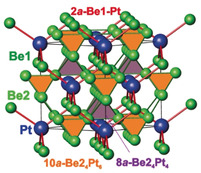
Semiconducting substances form one of the most important families of functional materials. However, semiconductors containing only metals are very rare. The chemical mechanisms behind their ground‐state properties are only partially understood. Our investigations have rather unexpectedly revealed the semiconducting behaviour (band gap of 190 meV) for the intermetallic compound Be5Pt formed at a very low valence‐electron count. Quantum‐chemical analysis shows strong charge transfer from Be to Pt and reveals a three‐dimensional entity of vertex‐condensed empty Be4 tetrahedrons with multi‐atomic cluster bonds interpenetrated by the framework of Pt‐filled vertex‐condensed Be4 tetrahedrons with two‐atomic polar Be−Pt bonds. The combination of strong Coulomb interactions with relativistic effects results in a band gap.
Keywords: beryllium, chemical bonding, intermetallic compounds, platinum, semiconductors
Progressive metals: Be5Pt is a rare representative of semiconductors that are formed by metallic elements only. The gap in the band structure appears due to both relativistic effects and a unique chemical‐bonding situation with polar two‐atom and multi‐atom Pt–Be interactions.
Introduction
From the first PbS rectifier to the Si‐based field‐effect transistor and light‐emitting diodes, semiconducting materials were crucial for the development of electronic devices, paving the way to the modern information age.[ 1 , 2 ] The continuous interest in new semiconducting materials is fuelled by the discovery of unexpected properties, which have led to emerging applications from thermoelectric materials with large Seebeck coefficients[ 3 , 4 ] to flexible electronics. [5] On the contrary, temperature‐driven semiconductor‐to‐metal transitions attract the interest of basic research. [6] Semiconducting behaviour in crystalline solids, caused by the existence of an energy gap at the Fermi level, can be rooted in several mechanisms. From the chemical point of view, the occurrence of semiconducting behaviour among intermetallic compounds relies heavily on i) the combination of elements, ii) the adopted crystal structure, and iii) the valence‐electron count. Since its discovery in the 1940s, [7] Mg2Sn represents this rather rare case. From the very beginning, its study has led to significant contributions to the scientific understanding of metals, alloys, and semiconductors.[ 8 , 9 , 10 , 11 ] The mechanism of gap formation is closely coupled to the type and spatial organisation of chemical bonding.
Most common semiconductors can be assigned to the group of so‐called tetrahedral structures, where all constituting atoms are fourfold (tetrahedrally) coordinated. Notable examples are the elemental semiconductors Si and Ge, with a diamond‐type crystal structure, and the thereof derived binary III–V and II–VI semiconductors GaAs, CdTe, ZnSe with sphalerite‐ or wurtzite‐type structures (Supporting Information, Table S1). In these “electron‐precise” compounds, an average count of four valence electrons per atom allows the formation of a three‐dimensional network of fourfold bonded atoms connected by two‐centre‐two‐electron covalent (polar) bonds.
Reduction of the average number of electrons below four may have different consequences, depending on the electronegativity difference between the components.[ 12 , 13 ] For large differences, intermetallic semiconductors follow the bonding scenario by Zintl.[ 14 , 15 ] Here, the cationic components donate their valence electrons to form two‐centre‐two‐electron covalent bonds only in the anionic sublattices of fourfold bonded (including lone pairs) atoms extended in three (intermetallic clathrates at appropriate compositions[ 16 , 17 , 18 , 19 ]), pseudo‐two (SrSi2), or zero (BaSi2) dimensions (Table S1). Ternary semiconductors with the CaAl2Si2‐type structure follow the Zintl scheme, for example, CaMn2Bi2 and CaCd2Sb2, although for the transition metals, only the s electrons are counted (Table S1). In all these substances, which typically contain Group 13–15 (p‐block) elements in the anionic part, the ionic interaction between the electron donors and the anionic sublattice completes the chemical bonding picture and supports the gap formation.
The appearance of a band gap in intermetallic compounds of the main‐group elements with XYZ composition and MgAgAs‐type crystal structure (half‐Heusler phases) can be described from the bonding point of view in three ways. Depending on the electronegativities of the components, it may either be ionic interaction between all three components as in LiMgN, or a Zintl‐like bonding picture as in LiAlSi, or a combination of non‐polar and polar characters of interactions still allowing the application of the Pearson 8−N rule. [20] In all cases, the cubic coordination of one of the components points to a more complex bonding picture. It can be described by a combination of polar three‐ and five‐centre interactions becoming evident for the half‐Heusler phases of transition metals, [21] for example, TiNiSn and TiCoSb (Table S1). As a general rule in half‐Heusler compounds, the Fermi level falls into the band gap at counts of 18 electrons per formula unit, assuming a closed‐shell configuration for the component in the cubic coordination. [22]
Another important group of semiconducting intermetallic compounds is formed by transition metals and Group 13–15 (p‐block) elements: MoSi2, CrSi2, RuGa2, OsAl2, MnCoAl4, as well as the Nowotny‐Chimney‐Ladder (NCL) phases Ru2Si3, Fe2Ge3, and ReGaSi (see Table S1). Characteristic for these substances is a relatively small electronegativity difference between the components, suggesting the formation of polar bonds. Indeed, despite the p‐block elements making up the majority of the composition, the direct interactions are mainly found between the transition‐metal and the p‐block atoms, for example, in ZrBi1.62. [23] For a valence‐electron count of 14 per formula unit with one transition metal, these compounds show distinct stabilization and are often found to be semiconducting. [24] Some intermetallic compounds with low average electron count and small electronegativity differences follow neither the 18‐ nor the 14‐electron count but are nevertheless (narrow‐gap) semiconductors: FeGa3, RuGa3, OsGa3, ZnSb, CdSb, or FeSi (Table S1). Here, the appearance of the gap is interpreted as the formation of several three‐centre interactions among the majority of two‐centre ones. [25]
In the case of large electronegativity difference and reduced average electron count, the formation of a band gap was observed when electron transfer formally leads to closed‐shell configurations for both partners, as in the semiconductors Mg2Si, Mg2Ge, and Mg2Sn which obey the Zintl count (Table S1). This exceptional behaviour also appears for combinations of the most electronegative with the most electropositive metals, with examples given by CsAu, RbAu, and Cs2Pt (Table S1). The charge transfer and the resultant presence of auride ions Au− ([Xe]6s24f145d10) was confirmed by photoemission and Mössbauer experiments.[ 26 , 27 ] Up to now, such behaviour was only reported for intermetallic semiconductors containing alkaline metals. Recently, strong charge transfer was observed in the Be‐rich complex intermetallic compound Be21Pt5. Its band structure already shows a small pseudo‐gap slightly above the Fermi level. [28] This was the motivation to search for semiconducting materials in the beryllium‐rich part of the Be–Pt system. The chemical challenge here is that the formed compounds challenge conventional valence‐counting rules due to the very low number of valence electrons per atom. The present work describes the interplay of two‐centre polar and multicentre covalent bonding which gives rise to the experimentally observed semiconducting ground state for the intermetallic compound Be5Pt (first observed in ref. [29] ) only when relativistic effects (already at the level of scalar‐relativistic treatment) are taken into account.
Results and Discussion
The compound Be5Pt adopts a crystal structure of the Be5Au type (space group F 3m, a=5.9710(3) Å) as observed from the X‐ray single‐crystal diffraction data (Figure 1, left, and Tables S1 and S2). The X‐ray powder‐diffraction pattern of the prepared product (Figure S1) confirms its single‐phase character. The lattice parameters of the Be5Pt phase in the samples with the off‐stoichiometric compositions are equal within three estimated standard deviations, which indicates a negligible homogeneity range.
Figure 1.
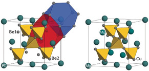
Crystal structures of Be5Pt (left) and MgCu2 (right). The Be2/Cu atoms (small grey spheres) form a network of vertex‐condensed tetrahedra (yellow). The Be1 atoms in Be5Pt replace half of the Mg positions in MgCu2, the second half (at the origin) is occupied by Pt atoms. Coordination polyhedra of Pt (large dark‐blue spheres) and Be1 (small grey spheres) are shown in blue and red, respectively (left).
The structural arrangement of Be5Au can be derived from the cubic one of the Laves phase MgCu2 (space group Fd m, Figure 1, right) by ordered occupation of the Mg positions (Wyckoff site 8a in Fd m) by Pt (site 4a in F 3m) and Be1 (site 4c in F 3m), respectively. From the structural point of view, Be5Pt does not reveal similarity to any specific family of semiconducting intermetallic compounds mentioned in the introduction. On the one hand, it does not show tetrahedral heteroatomic coordination for all atoms like in the classical III–V and II–VI semiconductors (while Pt and Be1 are fourfold coordinated by heteroatoms, Be2 has only 3 Pt atoms at the closest distance). On the other hand, it also does not contain isolated, zero‐, one‐, or two‐dimensional polyanions, characteristic for the Zintl phases or compounds like Mg2Si, CsAu, or Cs2Pt. Analysis of the interatomic distances suggests the formation of one substructure built of Pt tetrahedrally coordinated by Be1 at a distance of 2.59 Å (atomic radii of Pt and Be are 1.38 Å and 1.133 Å, respectively). Another substructure is formed by homo‐coordinated Be2 atoms, forming vertex‐condensed tetrahedra with relatively short distances of 2.09 Å (3×) and 2.13 Å (3×) with next‐nearest Pt atoms at 2.48 Å (in analogy to the Laves phases). Usually, the presence of such short distances in both substructures should be a fingerprint of covalent two‐centre interactions. The separation between the substructures—the Be1–Be2 distance of 2.48 Å—is larger than the Be2–Be2 distance and the distance of 2.08 Å in elemental beryllium, signalling a diversification of chemical interactions in Be5Pt. How justified the negligence or consideration of Be1–Be2 contacts is, will be discussed further in the context of chemical‐bonding analysis. The combination of high CN values (9 and 16) together with the very low number of valence electrons per atom signals diversification of chemical interactions in Be5Pt on the one hand and makes it an unlikely candidate for a semiconductor on the other hand.
The calculated electronic density of states (DOS) of Be5Pt reveals, quite unexpectedly, a narrow band gap of E g=85 meV (Figure 2) pointing towards semiconducting behaviour. The Pt 5d states dominate the valence band of Be5Pt between −7 and −4 eV. A special feature is the strong structuring of the Pt 5d contributions with several local maxima. The DOS within 3 eV below the Fermi level E F is dominated by Be 2p states.
Figure 2.
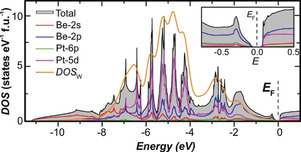
Calculated electronic density of states (DOS, fully relativistic treatment) for Be5Pt: total DOS, partial atomic contributions, and sum of the partial DOS weighted by photoionization cross‐sections and broadened for accounting for life‐time effects (DOSW) are shown as coloured lines; the inset shows details of the DOS around the Fermi level.
In contrast to the calculation results, the electrical resistivity measured on a bulk sample of Be5Pt shows a metal‐like temperature dependence (Figure 3 a). However, the microstructure of the sample (Figure 3 b) reveals small inclusions of elemental beryllium on the grain boundaries and within the grains, likely due to the peritectic formation of Be5Pt and existence of the Be–Be5Pt eutectic. Obviously, these metallic inclusions distort the results of the bulk measurement. In order to obtain information about the intrinsic conductivity, a microscale specimen was cut off from the single‐phase grain of the bulk sample with the focused‐ion‐beam technique [30] and provided with contacts to make a microdevice (Figure 3 c). The so‐measured electrical resistivity of Be5Pt decreases monotonically with increasing temperature, corresponding to a semiconducting behaviour inferred from the band‐structure calculations (Figure 3 d). The size of the band gap was estimated applying the Arrhenius relation ln ρ(T)=ρ 0 exp(−E g/2 k B T). A linear fit of ln ρ vs. 1/T in the temperature range from 335 K to 400 K (inset in Figure 3 D) yields a value of E g=190 meV for the energy gap. This is in a good agreement with results of the band‐structure calculations, particularly considering the typical underestimation of the band gap within the local‐density approximation.
Figure 3.
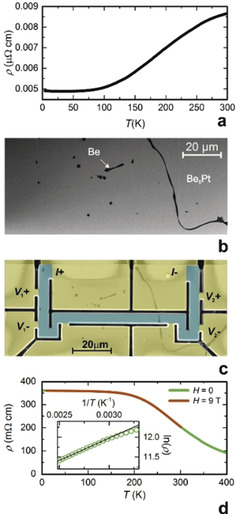
Electrical resistivity of Be5Pt: a) temperature dependence of electrical resistivity for the bulk sample; b) microstructure of the bulk sample showing inclusions of elemental beryllium; c) shape of the microscale device used for measurement (V and I are contacts for voltage and current, respectively); d) temperature dependence of electrical resistivity for the microscale samples; the inset shows an Arrhenius plot of ln ρ vs. 1/T with a linear fit (black line).
To substantiate the reasons behind the appearance of the band gap from a chemical point of view, analysis of chemical bonding was performed by applying quantum‐chemical techniques in position space. The calculated electron density was evaluated according to the quantum theory of atoms in molecules (QTAIM [31] ). In contrast to many other intermetallic compounds, the electron density in Be5Pt reveals two types of maxima. The “usual” maxima are located at the nuclei of the Pt and Be atoms, giving rise to the atomic basins (Figure 4 a). The so‐called non‐nuclear maxima (NNM) are located within the Be2 tetrahedra (Figure S2). Appearance of NNM was also observed for elemental lithium, [32] beryllium, [33] and some of their compounds. They were considered not as an exception, but as a normal evolution step of the chemical‐bonding picture in homonuclear groups with decreasing interatomic distances. [34] Fortunately for the further analysis, the basins of the NNM in Be5Pt have common surfaces mainly with those of Be2 atoms (Figure S2), that is, the Be2 atoms make the largest contribution to the population of the NNM basins. Thus, for the charge evaluation, the populations of the NNM basins were considered together with basins of Be2. Integration of the electron density within the QTAIM basins yields their electronic populations and after subtraction of the atomic numbers, the effective charges are obtained. These amount to −4.00 for Pt and +1.36 and +0.66 for Be1 and Be2 (Figure 4 a), respectively. This confirms the charge transfer from Be to Pt and the difference in the effective charge between Be species as identified by HAXPES (see below).
Figure 4.
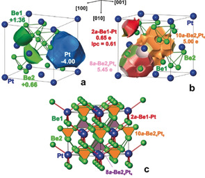
Chemical bonding in Be5Pt: a) shape of the atomic QTAIM basins and effective charges; b) bonding basins for the 2at Be1–Pt (red), multi‐atomic (10at) Be24Pt6 (orange), and 8at Be24Pt4 (light pink) interactions with their populations; lpc is the polar character of the 2at bond; c) general bonding picture in Be5Pt with the interpenetrating networks of multi‐atomic (Be2–Pt, green‐orange‐pink) and polar two‐atomic (Be1–Pt, red) interactions.
Further details of atomic interactions in Be5Pt were obtained from the topological analysis of the electron localisability indicator (ELI) in its ELI‐D representation (YD).[ 35 , 36 ] ELI‐D has recently developed into a powerful quantum‐chemical tool for the analysis of chemical bonding, particularly for intermetallic compounds.[ 20 , 21 , 36 , 37 ] The ELI‐D distribution reveals three types of bonding interactions in Be5Pt, visualised by three different types of attractors (ELI‐D maxima; Figures 4 b and S3). Two sets of ELI‐D attractors are located at the centres of the tetrahedra formed by Be2. The basins of attractors, centred at ( , , ) and ( , , ), have common surfaces with 8 and 14 atomic‐core basins. Having populations of 5.45 and 5.00 electrons, respectively, they represent multi‐atomic cluster bonds resulting from the low valence‐electron concentration, similar to the ones discovered recently in Be21Pt5. From the intersection analysis, the contribution of Be1 to the cluster bond pinned at ( , , ) is quite small (0.08 electrons, Table S4), so this cluster bond is considered as ten‐atomic (10a) instead of the 14‐atomic one, as it was found for Be21Pt5. [28] The basin of the cluster bond at ( , , ) does not reveal any contributions from the six neighbouring Be1 atoms, thus the interaction is an eight‐atomic (8a) one. The cluster bonds in Be5Pt interlink the (Be2)4 tetrahedrons with anionic Pt species.
A second type of interaction is visualised by the ELI‐D attractors located on the bond line between Pt and Be1 (basin population of 0.65 e−, Figure 4 b and Table S4). Their basins have only contributions from Pt (0.51 e−) and Be1 (0.12 e−) with negligible amount of 0.02 e− from six Be2, so it is a two‐atomic (2a) interaction. The polar character lpc of 0.61 for this bond qualifies it as a strongly polar one (lpc=0 represents a non‐polar bond, lpc=1 reflects a fully polar (closed‐shell) interaction [22] ). Charge transfer from Be to Pt, caused by this interaction, leads to filling and energy lowering of the Pt 5d states[ 26 , 27 ] (see the findings of the HAXPES experiments below). These polar 2a‐Be1−Pt bonds stretch the substructure with tetrahedrally bonded platinum and beryllium atoms.
Interestingly, there are no special topological features in the ELI‐D distribution between Be1 and Be2 in Be5Pt (Figure S4). Such behaviour is characteristic of a non‐bonding interaction caused by the repulsion of the positively charged beryllium species due to the strong bond polarity of Be–Pt interactions.
Aside from the charge transfer, relativistic effects were suggested to support the opening of the gap in the DOS for polar intermetallic compounds. [38] In order to investigate this issue, fully, scalar‐, and non‐relativistic calculations were performed for Be5Pt, Be5Pd, and hypothetical Be5Ni. However, only the relativistic calculation for Be5Pt yields the narrow band gap (Figures 2 and S7). Accounting for relativistic effects increases the charge transfer (Figure S5), increases the population of the 2a‐Be1–Pt interaction, and reduces the populations of both multi‐centre cluster bonds (Figure S6, Table S4), that is, the bonding appears to be more covalent in the relativistic approximation which leads to band narrowing and an opening of the gap. This effect is much smaller for Be5Pd and practically disappears for the hypothetical Be5Ni. The most striking effect of relativity is on the interactions between Be1 and Be2. In the semiconducting Be5Pt, the Be1 contributions to the cluster bonds and the Be2 contributions to the 2a‐Be1–Pt bonds are negligible. When going from Be5Pt to Be5Ni and from relativistic to non‐relativistic treatments, the Be1 participation in the cluster bonds increases (Table S4), implying more attractive interactions between Be1 and Be2 species. Further confirmation was provided by the presence of semiconducting behaviour and increase of the band gap up to 0.44 eV in Be5MgPt—a hypothetical composition with a larger component‐electronegativity difference than in Be5Pt (Figure S8). In contrast, the electronic structure of the prototype Be5Au is typical for a metal (Figure S10).
To shed more light on the reasons for the appearance of semiconducting behaviour in Be5Pt, the electronic structure of the valence‐band and core levels was investigated by hard X‐ray photoelectron spectroscopy (HAXPES). The valence‐band spectrum of Be5Pt (Figure 5 a) is in good agreement with the calculated density of states weighted by photoionization cross‐sections DOSW (Figure 2). The localised Pt 5d levels are shifted well below E F compared to Pt metal. Around the Fermi level, the HAXPES spectrum shows a strongly reduced intensity and a clear shift of the onset compared to Pt metal, confirming the absence of occupied states (insets in Figures 5 a and 2). The Pt 4f core levels in Be5Pt are shifted to higher binding energies E bind by +2.12 eV compared to Pt metal (Figure 5 b). Concomitantly, the peak shape changes from an asymmetric one in Pt metal to a symmetric one in Be5Pt, in line with a transition from metallic to semiconducting behaviour. From electronegativity (EN) arguments (on the Pauling scale: EN(Pt)=2.2, EN(Be)=1.57 [39] ) and the quantum‐chemical calculations (see above), a charge transfer from Be to Pt is expected. The more complete filling of the Pt 5d valence shell enhances the shielding of the core hole on Pt and reduces relaxation from the valence band. In metals, this effect is of a similar magnitude to the chemical shift, hindering straightforward deduction of charge transfer from core‐level shifts. [40] Additionally, the filling of Pt 5d states shifts the core levels to higher binding energies. Thus, this does not equate to a chemical shift due to a positive charge on Pt but supports the notion of filling of the Pt 5d states, analogous to the effect observed in Ga–Pd intermetallic compounds. [41] In the HAXPES spectra of the Be 1s core level, unexpectedly, two lines were observed which are separated by ΔE bind=1.68 eV (Figure 5 c). Both lines are shifted to higher binding energies, compared to Be metal (E bind=111.3 eV [42] ). The s‐character of both lines was confirmed by the line‐intensity variation between spectra recorded with the electron analyser in parallel and perpendicular orientation relative to the polarization plane of the incident beam (for details, see the Materials and Methods section in the Supporting Information). The peak‐area ratio of the two lines at 113.86 eV and 112.18 eV is approximately 1:4.3. This corresponds closely to the atomic ratio of the Be1 (fourfold site) and Be2 (sixteenfold site) in the crystal structure of Be5Pt. Electronic structure calculations reproduced the separation of the Be1 and Be2 core levels, yielding a ΔE bind of 1.55 eV (well in agreement with the experimental value above). This is strong evidence for a vastly different atomic environment and chemical bonding of Be1 and Be2 (see the crystal structure and chemical‐bonding analysis above). Assuming that final‐state effects are comparable for both sites, the higher binding energy on Be1 may be interpreted as a more positive effective charge on Be1 than on Be2 (see the QTAIM results above). All in all, the good agreement of the experimental valence‐band spectrum of Be5Pt (Figure 5 a) with the calculated density of states weighted by photoionization cross‐sections DOSW (Figure 2) as well as the correct explanation of the Pt and Be core levels justifies the reliability of the calculation results and, indirectly, confirms the presence of the negatively charged platinum species in the structure as obtained from the analysis of chemical bonding above.
Figure 5.
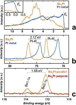
Hard‐X‐ray photoelectron spectra of Be5Pt: a) valence band (orange) in comparison with Pt metal (blue), the inset shows a detailed view around E F; b) Pt 4f core levels (orange) in comparison with Pt metal (blue); c) polarization‐dependent Be 1s core‐level spectra of the Be1 and Be2 positions recorded in parallel (orange) and perpendicular (pink) detector geometry.
Conclusion
The binary compound Be5Pt is a rare representative of semiconductors that are formed by metallic elements only. The appearance of the gap in the band structure is a consequence of the relativistic effects and the unique chemical‐bonding situation in the compound characterised by polar two‐atomic Pt–Be1 and multi‐atomic Pt–Be2 bonds. In fact, the combination of charge transfer caused by the electronegativity difference between the components and relativistic effects controls the semiconducting behaviour.
Conflict of interest
The authors declare no conflict of interest.
Supporting information
As a service to our authors and readers, this journal provides supporting information supplied by the authors. Such materials are peer reviewed and may be re‐organized for online delivery, but are not copy‐edited or typeset. Technical support issues arising from supporting information (other than missing files) should be addressed to the authors.
Supplementary
Acknowledgements
The authors acknowledge Andrew P. Mackenzie and Frank R. Wagner for valuable discussions. The HAXPES measurements were facilitated by the Max Planck‐POSTECH Hsinchu Centre for Complex Phase Materials. Open access funding enabled and organized by Projekt DEAL.
A. Amon, E. Svanidze, A. Ormeci, M. König, D. Kasinathan, D. Takegami, Y. Prots, Y.-F. Liao, K.-D. Tsuei, L. H. Tjeng, A. Leithe-Jasper, Y. Grin, Angew. Chem. Int. Ed. 2019, 58, 15928.
References
- 1. Bose J. C., Proc. R. Soc. London 1900, 65, 166–172. [Google Scholar]
- 2. Venema L., Nature 2011, 479, 309–309. [DOI] [PubMed] [Google Scholar]
- 3. Bentien A., Johnsen S., Madsen G. K. H., Iversen B. B., Steglich F., Europhys. Lett. 2007, 80, 17008. [Google Scholar]
- 4. Sales B. C., May A. F., McGuire M. A., Stone M. B., Singh D. J., Mandrus D., Phys. Rev. B 2012, 86, 235136. [Google Scholar]
- 5. Shi X., Chen H., Hao F., Liu R., Wang T., Qiu P., Burkhardt U., Grin Y., Chen L., Nat. Mater. 2018, 17, 421–427; [DOI] [PubMed] [Google Scholar]; Shi X., Chen H., Hao F., Liu R., Wang T., Qiu P., Burkhardt U., Grin Y., Chen L., Nat. Mater. 2019, 18, 652. [DOI] [PubMed] [Google Scholar]
- 6. Anisimov V. I., Ezhov S. Y., Elfimov I. S., Solovyev I. V., Rice T. M., Phys. Rev. Lett. 1996, 76, 1735–1738. [DOI] [PubMed] [Google Scholar]
- 7. Robertson W. D., Uhlig H. H., Trans. Am. Inst. Min. Metall. Eng. 1948, 180, 345–355. [Google Scholar]
- 8. Mott N. F., Jones H., Theory of Metals and Alloys Clarendon Press, Oxford, 1936. [Google Scholar]
- 9. Welker H., Physica 1954, 20, 893–909. [Google Scholar]
- 10. Welker H., Ergeb. Exakten Naturwiss. 1956, 29, 275–343. [Google Scholar]
- 11. Mooser E., Pearson W. B., Acta Crystallogr. 1959, 12, 1015–1022. [Google Scholar]
- 12. Lin Q., Miller G. J., Acc. Chem. Res. 2018, 51, 49–58. [DOI] [PubMed] [Google Scholar]
- 13. Grin Y., Comprehensive Inorganic Chemistry II, Vol. 2, Elsevier, Oxford, 2013, pp. 359–373. [Google Scholar]
- 14. Zintl Phases: Principles and Recent Developments (Structure and Bonding) (Ed.: Fässler T. F.), Springer, Heidelberg, 2011. [Google Scholar]
- 15. Chemistry, Structure, and Bonding of Zintl Phases and Ions (Ed.: Kauzlarich S.), Wiley, New York, 1996. [Google Scholar]
- 16. Kovnir K. A., Shevelkov A. V., Russ. Chem. Rev. 2004, 73, 923–938. [Google Scholar]
- 17. Nolas G. S., Cohn J. L., Slack G. A., Schujman S. B., Appl. Phys. Lett. 1998, 73, 178–180. [Google Scholar]
- 18. Ormeci A., Grin Y., J. Thermoelectr. 2015, 6, 16–32. [Google Scholar]
- 19. Bhattacharya A., Carbogno C., Böhme B., Baitinger M., Grin Y., Scheffler M., Phys. Rev. Lett. 2017, 118, 236401. [DOI] [PubMed] [Google Scholar]
- 20. Wagner F. R., Bende D., Grin Y., Dalton Trans. 2016, 45, 3236–3243. [DOI] [PubMed] [Google Scholar]
- 21. Bende D., Grin Y., Wagner F. R. in Heusler Alloys (Eds.: Felser C., Hirohata A.), Springer, Heidelberg, 2016, p. 133. [Google Scholar]
- 22. Graf T., Felser C., Parkin S. S. P., Prog. Solid State Chem. 2011, 39, 1–50. [Google Scholar]
- 23. Boström M., Lind H., Lidin S., Niewa R., Grin Y., Solid State Sci. 2006, 8, 1173–1180. [Google Scholar]
- 24. Fredrickson D. C., Lee S., Hoffmann R., Inorg. Chem. 2004, 43, 6159–6167. [DOI] [PubMed] [Google Scholar]
- 25. Wang S., Yang J., Wu L., Wei P., Yang J., Zhang W., Grin Y., Chem. Mater. 2015, 27, 1071–1081. [Google Scholar]
- 26. Jansen M., Solid State Sci. 2005, 7, 1464–1474. [Google Scholar]
- 27. Jansen M., Chem. Soc. Rev. 2008, 37, 1826–1835. [DOI] [PubMed] [Google Scholar]
- 28. Amon A., Ormeci A., Bobnar M., Akselrud L., Avdeev M., Gumeniuk R., Burkhardt U., Prots Y., Hennig Ch., Leithe-Jasper A., Grin Y., Acc. Chem. Res. 2018, 51, 214–222. [DOI] [PubMed] [Google Scholar]
- 29. von Batchelder F. W., Raeuchle F., Acta Crystallogr. 1958, 11, 122. [Google Scholar]
- 30. Moll P. J. W., Kushwaha P., Nandi N., Schmidt B., Mackenzie A. P., Science 2016, 351, 1061–1064. [DOI] [PubMed] [Google Scholar]
- 31. Bader R. F. W., Atoms in Molecules—A Quantum Theory, Oxford, Clarendon Press, 1995. [Google Scholar]
- 32. Luaña V., Mori-Sánchez P., Costales A., Blanco M. A., Martin-Pendás A., J. Chem. Phys. 2003, 119, 6341–6350. [Google Scholar]
- 33. Martin-Pendás A., Blanco M. A., Costales A., Mori-Sánchez P., Luaña V., Phys. Rev. Lett. 1999, 83, 1930–1933. [Google Scholar]
- 34. Kohout M., Faraday Discuss. 2007, 135, 43–54. [DOI] [PubMed] [Google Scholar]
- 35. Wagner F. R., Bezugly V., Kohout M., Grin Y., Chem. Eur. J. 2007, 13, 5724–5741. [DOI] [PubMed] [Google Scholar]
- 36. Bende D., Wagner F. R., Sichevych O., Grin Y., Angew. Chem. Int. Ed. 2017, 56, 1313–1318; [DOI] [PubMed] [Google Scholar]; Angew. Chem. 2017, 129, 1333–1338. [Google Scholar]
- 37. Wagner F. R., Cardoso-Gil R., Boucher B., Wagner-Reetz M., Sichelschmidt J., Gille P., Baenitz M., Grin Y., Inorg. Chem. 2018, 57, 12908–12919. [DOI] [PubMed] [Google Scholar]
- 38. Pyykkö P., Annu. Rev. Phys. Chem. 2012, 63, 45–64. [DOI] [PubMed] [Google Scholar]
- 39. Emsley J., The Elements, Oxford University Press, Oxford, 1999. [Google Scholar]
- 40. Wertheim G. K., Buchanan D. N. E., Wernick J. H., Phys. Rev. B 1989, 40, 5319–5324. [DOI] [PubMed] [Google Scholar]
- 41. Armbrüster M., Schlögl R., Grin Y., Sci. Technol. Adv. Mater. 2014, 15, 034803. [DOI] [PMC free article] [PubMed] [Google Scholar]
- 42. Höchst H., Steiner P., Hüfner S., Phys. Lett. A 1977, 60, 69–71. [Google Scholar]
Associated Data
This section collects any data citations, data availability statements, or supplementary materials included in this article.
Supplementary Materials
As a service to our authors and readers, this journal provides supporting information supplied by the authors. Such materials are peer reviewed and may be re‐organized for online delivery, but are not copy‐edited or typeset. Technical support issues arising from supporting information (other than missing files) should be addressed to the authors.
Supplementary


