

Abstract

The asymmetric n-type Ph-BTBT-C10 derivative 2-decyl-7-phenyl-[1]benzothieno[3,2-b][1]benzothiophene S,S,S′,S′-tetraoxide is structurally investigated in the thin film regime. After film preparation by spin coating and physical vapor deposition, a rather disordered structure is observed, with a strong change of its internal degree of order upon heating. At 95 °C, a transition into a layered structure of upright standing molecules without any in-plane order appears, and at 135 °C, crystallization takes place. This phase information is combined with surface morphological studies and charge carrier mobility measurements to describe the structure and thin film transistor applicability of this molecule.
Short abstract
The asymmetric n-type Ph-BTBT-C10 derivative 2-decyl-7-phenyl-[1]benzothieno[3,2-b][1]benzothiophene S,S,S′,S′-tetraoxide is structurally investigated in the thin film regime. A phase transition behavior during heating of BTBTOx2 thin films occurs. A two-step transition is described with cold crystallization occurring at 135°C.
Introduction
Since more than a decade, [1]benzothieno[3,2-b]benzothiophene (BTBT) derivatives are fueling hopes in the field of solution processable small molecule organic semiconductors showing record charge carrier mobilities, stability, and high solubility.1−3 With their low reorganization energies and large transfer integral in multiple directions, they have proven that molecules with an extended aromatic core and solubilizing long aliphatic chains have a favorable molecular design.4−6 Studies on the symmetrical C8-BTBT-C8 and C12-BTBT-C12 have shown impressive hole mobilities surpassing 5 cm2 V–1 s–1, further highlighting a common trait in organic semiconductors, i.e., a deep relation between structure and electrical properties.7−15 The arrangement of the molecules in the solid state and their relative orientation with respect to the substrate determine the π orbital overlap and thereby the electrical performance.13,16 While the investigation of rigid and symmetric molecules dominated earlier approaches, the focus has recently shifted toward asymmetric molecules.17−20 Ph-BTBT-C10, for example, has shown how a precise control of phase formation can isolate favorable herringbone structures, forming films with high p-type mobilities of 10 cm2 V–1 s–1, homogeneous morphology, and great thermal stability.21−26 Research on n-type organic semiconductors has been lagging behind the progress in p-type, although they are indispensable components for complementary integrated circuits. Electron-transporting molecules are relatively sophisticated to synthesize and often limited in stability under ambient conditions.27 Recently, the first unipolar n-type BTBT based device has been proposed and probed, showing a complex structure with relatively high electron mobilities of ∼0.6 cm2/(V s).28 We present here studies on another electron-transporting BTBT derivative, a substructure of Ph-BTBT-C10: 2-decyl-7-phenyl-[1]benzothieno[3,2-b][1]benzothiophene S,S,S′,S′-tetraoxide (BTBT-Ox2). The design of the molecule is based on recent evidence suggesting a transition from the p-type to the n-type regime in BTBT like structures during oxidation of the two sulfur atoms to sulphones.29 This study presents structural investigations on thin films prepared by different deposition methods and at different temperatures. A focus is proposed on the distinction of unique phases and the observation of their morphology and charge transport properties.
Experimental Section
The films for structural investigations were prepared by spin coating and Physical Vapor Deposition (PVD). Both methods involve processes far from equilibrium, favoring the formation of metastable states. As substrates, 1 × 1 cm2 Si wafers with a 150 nm thermal oxide layer were used. They underwent a cleaning routine, comprising ultrasonication in acetone for 10 min and subsequent rinsing with isopropanol to remove potential residues. According to contact angle measurements with different solvents, the surface energy after cleaning is 49.7 mJ m–2, with 25.3 mJ m–2 for the dissipative part and 24.4 mJ m–2 for the polar part, suggesting a hydrophilic surface.
BTBT-Ox2 was synthesized directly from Ph-BTBT-C10 by oxidation with m-chloroperbenzoic acid in a dichloromethane solution. The chemical structure of the molecule is shown in Figure 1. It features a phenyl group and a decyl chain in the 7- and 2-positions, respectively. The high oxidation state of the sulfur atoms confirms the n-type characteristic, i.e., its large electron affinity, of the molecule.29
Figure 1.

Chemical structure of the molecule BTBT-Ox2.
For spin coating, the molecule was dissolved into toluene, varying
the solute concentration between 0.5 and 5 g/L. The spin speed and
amount of solution used during spinning were fixed at 1000 rpm and
90 μL, respectively. Samples prepared by PVD were fabricated
in a tabletop evaporator inside an argon glovebox. The material was
heated in Wolfram evaporation boats at a base pressure of 10–6 mbar. Deposition rates were kept constant at 1 nm/min, monitored
by a quartz crystal microbalance located close to the substrate. The
deposition thickness was chosen between 24 and 307 Å.30 The films were characterized by four different
X-ray based methods: Specular X-ray Diffraction (XRD), specular X-ray
Reflectivity (XRR), Grazing X-ray Diffraction (GIXD) and synchrotron
powder diffraction measurements. The specular measurements (XRD and
XRR) were performed on a PANalytical Empyrean diffractometer operating
at a wavelength of λ = 1.542 Å. On the primary side, the
latter is equipped with a sealed cooper tube, together with a multilayer
mirror, to create a parallel beam. On the secondary side, it has a
receiving slit, a 0.02 rad Soller slit, and a PANalytical PIXcel 2D
detector. The angular measurements (2θ) were transformed to
reciprocal space using the formula  , with qz representing the scattering
vector perpendicular to the substrate.
The real space planes distance d depends on qz according to the formula
, with qz representing the scattering
vector perpendicular to the substrate.
The real space planes distance d depends on qz according to the formula  . The
XRR measurement data were fitted with
the Parratt formalism,31 incorporating
the surface roughness by the Névot and Croce approach.32
. The
XRR measurement data were fitted with
the Parratt formalism,31 incorporating
the surface roughness by the Névot and Croce approach.32
GIXD measurements took place at the Elettra synchrotron facility on two different beamlines, namely, the XRD1 and the SAXS beamlines.33 In both cases, the incidence angle αi was chosen at the critical angle of total external reflection αc to suppress the signal from the amorphous SiO2. At room temperature, the measurements were performed on the XRD1 beamline with an operating wavelength of 1.400 Å and beam dimension of 400 μm2. The beamline uses a stationary Dectris Pilatus 2M detector. At elevated temperatures, in situ variable temperature measurements were performed on the SAXS beamline with a wavelength of 1.54 Å and beam dimension of 400 μm2. The beamline is equipped with an Anton Paar DHS 1100 heating stage, enabling a precise temperature control during the measurements.34 A Dectris Pilatus 1M served as the detector. All GIXD measurement data were evaluated with the GIDVis software package,35 creating two-dimensional contour plots with a linearly scaled color code ranging from blue, representing low intensity, to yellow, representing high intensity. The powder diffraction measurements were performed at the XRD2 beamline of the Elettra Synchrotron.33 Polycrystalline thin films fragments were dipped in NHV oil and mounted on the goniometer head with kapton loops. The data sets were collected at room temperature by rotating the samples by 360° to achieve radially homogeneous powder patterns, without preferential orientations. A monochromatic wavelength of 0.620 Å was used onto a Pilatus 6M hybrid-pixel area detector at a working distance of 290 mm, using a 100 μm aperture. The powder diffraction patterns were integrated using the Fit2D program36,37 after calibrating the hardware setup with LaB6 standard reference powder (NIST 660a).
The atomic force microscopy (AFM) measurements at room temperature were performed on a Nanosurf Easyscan 2 modular scanning probe system. This system has a maximum scan range of 70 μm ± 15%, a maximum z-range of 14 μm, a drive resolution in z of 0.21 nm and in xy of 1.1 nm. AFM measurements were performed in tapping mode. The Easyscan 2 operates with a scan speed up to 60 ms/line at 128 data points/line. The sensing cantilever attached to the head was a PPP-NCLR silicon-spm-sensor tip. All AFM data were processed with the Gwyddion software package.38
The charge carrier mobility of the films
was evaluated by fabricating
bottom-gate field-effect transistors with bottom contacts. Si substrates
with a thermal oxide layer of 230 ± 10 nm and pre-patterned source
and drain gold electrodes were used. The charge mobility was extracted
from the measured transfer curves of the transistors, biased in the
saturation regime at a gate (Vg) and drain
(Vd) voltage of 60 V. From Vg, the drain current Id, the
channel length L and width W, and
the gate dielectric capacitance Cdiel,
the charge mobility was calculated using the formula  .39 All charge
carrier mobility measurements were performed at room temperature and
in an inert atmosphere, including measurements on the high temperature
phases, which were rapidly cooled down to 25 °C to preserve their
order.
.39 All charge
carrier mobility measurements were performed at room temperature and
in an inert atmosphere, including measurements on the high temperature
phases, which were rapidly cooled down to 25 °C to preserve their
order.
Results
Initially, as-deposited films at room temperature show a rather disordered phase.
The XRR curves in Figure 2a demonstrate the film formation for different spin-coating solute concentrations (blue) and PVD deposition thicknesses (light blue). The curves show oscillations, so-called Kiessig fringes, which are related to the homogeneity of the deposited film. While the spin-coated films grow at low concentrations with pronounced fringes that lose their characteristics toward 5 g/L, the PVD films form less pronounced ones throughout the growth. The curves were fitted (red curves) up to the point where the broad Bragg peak influences the reflectivity signal. Film density and film roughness values specific to each grown layer are given in Table 1, on the basis of single layer models. For the spin-coated samples, the density initially increases together with the layer thickness and roughness, and then decreases again toward 5 g/L. This suits very well an initial high coverage growth, with limited vacancies, at lower concentrations, with instead trenches at higher thicknesses, decreasing the coverage and layer density. PVD shows similar XRR fitting results but with a stronger roughening throughout the growth. At a low PVD thickness of 60 Å, the fit is similar to the coated layer at 0.7 g/L, with only the density hinting toward a reduced coverage. As the films get thicker, the difference gets stronger, especially in roughness. The fits suit to a strong island growth, where the island density at the surface increases toward higher thickness. Both cases are in accordance with the AFM images discussed later.
Figure 2.

X-ray scattering on BTBT-Ox2 thin films in the as-deposited state at 25 °C. (a) Specular X-ray reflectivity (XRR) of spin-coated films prepared with different solute concentrations and physical vapor deposited films with different film thicknesses. (b) Grazing incidence X-ray diffraction of a 5 g/L spin-coated film with an XRR thickness of 221 Å.
Table 1. X-ray Reflectivity Fitting Parameters of Thin Films Prepared by Different Spin-Coating Concentrations and PVD Deposition Thicknesses Together with the Roughness from the AFM Measurements σRMS and the Crystal Height from the XRD Peak Width Analysis.
| spin
coating | |||||
|---|---|---|---|---|---|
| concentration (g/L) | density (g/cm3) | thickness (Å) | roughness (Å) | crystal height (Å) | AFM σRMS (Å) |
| 0.7 | 1.0 | 25 | 8 | 6 | |
| 1 | 1.2 | 50 | 3 | 5 | |
| 2 | 1.2 | 93 | 15 | 10 | |
| 3 | 1.1 | 140 | 22 | 140 | |
| 5 | 1.0 | 221 | 30 | 200 | 63 |
| physical
vapor deposition | |||||
|---|---|---|---|---|---|
| nominal thickness (Å) | density (g/cm3) | thickness (Å) | roughness (Å) | crystal height (Å) | AFM σRMS (Å) |
| 60 | 0.7 | 24 | 4 | 26 | |
| 94 | 1.0 | 87 | 23 | 33 | |
| 133 | 1.0 | 115 | 45 | 51 | |
| 307 | 1.1 | 270 | 36 | 280 | 22 |
Another notable feature in the XRR curves is the broad Bragg peak at qz = 0.443 Å–1. It originates from the periodic packing of the molecules parallel to the surface, and its peak width includes information about the crystal size in the vertical direction. At 3 g/L, 5 g/L, and 307 Å, the peaks were fitted with the slit interference function, as shown in Figure 2a. The fittings return similar film thicknesses compared to the XRR measurements and are reported in Table 1 as the crystal height.
Despite the layer growth being significantly different for the two deposition methods, they create a comparable crystalline phase. Its characteristic features include the mentioned Bragg peak in the specular direction at qz = 0.443 Å–1 and intensities in the in-plane direction visible in the GIXD measurements in Figure 2b. The latter include a broad intensity spot at qxy = 0.95 Å–1/qz = 1.27 Å–1 elongated in qz by about 0.5 Å–1, as well as a Bragg rod at qxy = 0.86 Å–1 and a weaker one at qxy = 1.56 Å–1. These features are characteristic for 2D crystallites aligned parallel to the substrate surface.
Directly after deposition by spin coating and PVD at room temperature, the same disordered phase is observed with two different growth morphologies.
A phase transition occurs as the samples are heated above 95 °C. The new structure has strong and broad out-of-plane Bragg peaks at qz = 0.21 Å–1 and corresponding higher orders, as shown in Figure 3a, where data of in situ XRR measurements during heating at 95 °C are reported.
Figure 3.

X-ray based studies of BTBT-Ox2 thin films during heating at 95 °C. (a) Specular XRR measurement of a spin-coated and a physical vapor deposited film. (b) GIXD image of a film spin-coated with a concentration of 5 g/L.
This relates to a net-plane distance of 29.7 Å, which is about the long axis molecular length. The Kiessig fringes present at room temperature disappear completely. The in situ GIXD measurements during heating at 95 °C do not show clear peaks in the in-plane direction, neither for the spin-coated nor for the physical vapor deposited samples (Figure 3b). There is instead evidence of periodic order in the out-of-plane direction, with an interplanar distance corresponding to upright standing molecules, without any observable defined crystallographic order in the lateral direction. This evidence suits very well a structure in which the molecules stack forming defined layers, but do not arrange toward each other interplanarly within the layers. Short-range order arrangements however cannot be excluded.
A second phase transitions is observed after further increasing the temperature to 135 °C. The in situ XRR measurements at 135 °C shown in Figure 4a have pronounced Kiessig fringes at low angles, indicating the presence of defined layers. They were fitted (red) for the spin-coated sample to a layer of 55 Å, with a roughness of 6 Å, and for the PVD sample to a layer of 43 Å, with a roughness of 5 Å. In both cases, a crystalline order with sharp out-of-plane Bragg peaks and defined in-plane intensities is found, as illustrated in Figure 4.
Figure 4.

X-ray based characterization of BTBT-Ox2 thin films during heating at a temperature of 135 °C. (a) Specular XRR of a spin-coated and a physical vapor deposited film. (b) GIXD pattern of a film spin-coated at 5 g/L. The white circles indicate calculated peak positions and peak intensities of the solved crystal structure. (c) Packing of the molecules within the crystallographic unit cell. (d) Arrangement of the molecules relative to the substrate surface.
In the specular direction, a sharp Bragg peak is observed at qz = 0.57 Å–1, corresponding to an interplanar distance of 11 Å (Figure 4a). In situ GIXD measurements during heating at a temperature of 135 °C (Figure 4b) have defined intensities in the in-plane direction, with the strongest peak along qxy = 0.80 Å–1. This is indicative for crystalline order. The crystal structure solution proposed in Figure 4c has a noncentrosymmetric triclinic unit cell. Its parameters are given in Table 2. The structure suggests that the BTBT-Ox2 molecules pack in a compact phase with two independent molecules in the asymmetric unit, without any solvent molecule inclusions.
Table 2. Unit Cell Parameters of the Solved Crystal Structure Solution (CCDC 1999373).
| cell lengths (Å) | cell angles (deg) | ||
|---|---|---|---|
| a | 8.563(1) | α | 68.29(1) |
| b | 12.398(1) | β | 86.46(1) |
| c | 14.397(2) | γ | 77.21(1) |
| cell volume (Å3) | space group | ||
|---|---|---|---|
| 1384.5(3) | P1(1) |
The obtained crystal structure is able to index the peaks present in the thin film regime very well as shown in Figure 4b. The peak positions and intensities match with the measurements for a preferential growth of the 011 plane parallel to the substrate surface as illustrated in Figure 4d. This arrangement has a π–π stacking distance of ∼3.7 Å, with the aromatic cores inclined by ∼24.2° to the surface and slightly tilted toward each other by ∼7.3°.
Morphology
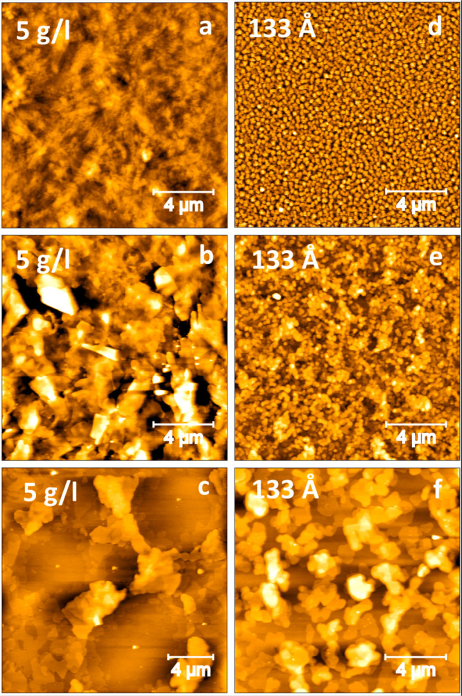
To gain topographic insight in the thin film morphology, AFM height measurements were performed. Representative micrographs after sample preparation at 25 °C are given in Figure 5 for different spin-coating concentrations and PVD thicknesses. Although they have identical crystalline order, the morphological differences are striking. The spin-coated samples have a strong coverage for the first two layers and a subsequent terrace like growth toward higher concentrations (a)–(d). This is in accordance with the XRR fits in Table 1 when considering that the density and roughness values are connected to the coverage visible in the AFM images. The spin-coated films show a mound growth in which the surface coverage and layer density first increase and then decrease due to strong roughening and the formation of trenches. The PVD samples, on the other hand, show a strong island growth with an increasing island density on the surface toward longer deposition times (e)–(h). This agrees with the XRR fits in which the layer density is initially low but increases rapidly with the thickness and roughness (Table 1).
Figure 5.

Morphological characterization of BTBT-Ox2 thin films by atomic force microscopy after deposition as prepared at 25 °C. (a–d) Spin-coated films in a concentration range from 0.5 to 2 g/L (z-scale ranging from 0 black to 8.3 nm white). (e–h) Physical vapor deposited films with thicknesses between 24 and 304 Å (z-scale ranging from 0 black to 17 nm white).
To measure the topography of the two elevated temperature phases, some samples were rapidly cooled down to room temperature after heating over the respective transition temperature of 95 and 135 °C. Thereby, the phase is stabilized to room temperature and the surface could be studied by AFM. The morphology changes significantly after the thermally induced transitions, as shown in Figure 6. For the spin-coated samples, the trenches close after the transition and the terraces join into more planar layers at 95 °C (b). The island size increases significantly. This trend continues for the second transition at 135 °C (c). The PVD samples undergo an island agglomeration into bigger structures when heated above 95 °C (e). After the second phase transition at 135 °C, the surface morphology changes even further (f), leaving several micrometer large structures spread over the surface.
Figure 6.
Morphological characterization by AFM before and after heat treatment: (a) Spin-coated with a concentration of 5 g/L at 25 °C as prepared. (b) Heated to 95 °C and then rapidly cooled to 25 °C. (c) Heated to 135 °C and then rapidly cooled to 25 °C. (d) PVD deposited samples at 25 °C as prepared. (e) Heated to 95 °C and then rapidly cooled to 25 °C. (f) Heated to 135 °C and then rapidly cooled to 25 °C (z-scale range from 0 black to 50 nm white).
Charge Carrier Mobility
The charge carrier mobility was investigated in field-effect transistors (FETs). The FET electrical characteristics of the room temperature phase, obtained directly after deposition, and of the phase obtained by annealing at 95 °C are below our measurement limit. As a consequence, a mobility cannot be assessed, and only a higher limit of 10–7 cm2 V–1 s–1 can be estimated. However, a clear field-effect current modulation is measured for the transistors where the channel is based on samples that underwent the phase transition at 135 °C. Measurements indicate an electron mobility of ∼10–5 cm2 V–1 s–1 (measured in the saturation regime of operation at Vd = Vg = 60 V). The thin film transistor turns on at an applied gate voltage Vg of about 20 V (Figure 7) with a reasonably low gate leakage (Ig) compared to the channel current (I). The transfer curve measurements suggest the presence of trapping effects at the interface with the dielectric or in the bulk layer. We investigated the possibility of reducing the influence of trapping sites at the dielectric interface by passivating the surface with a self-assembled monolayer of hexamethyldisilazane prior to the semiconductor deposition. No appreciable difference was detected in the latter case, compared to the case with an unpassivated surface. A rather limited in-plane connectivity of the crystals, grain boundaries, and other interfacial effects can be responsible for the modest electron mobility measured.
Figure 7.

Transfer characteristic curve and extracted charge carrier mobility for a heat-treated thin film of the molecule BTBT-Ox2 measured in a bottom gate – bottom contact FET configuration in the saturation regime at Vd = Vg = 60 V.
Discussion
BTBT-Ox2 grows with a very different morphology for the two deposition methods, while the crystallographic features and the phase transition behavior are comparable. Spin coating leads to an initial closed layer growth, followed by a moderate mound formation with vacant trenches in-between, while PVD induces a strong island growth starting from the first monolayer onward. Toward higher thicknesses, the island density increases, maintaining a strongly fragmented surface. The XRR fits and AFM measurements agree well when considering that the fitted layer density and roughness are connected to the layer coverage.
The prepared thin films have three different stable phases with distinct crystalline order involving two phase transitions at elevated temperatures. The first phase appears directly after deposition at room temperature, the second forms at 95 °C, and the third appears at 135 °C. Both elevated temperature phases were investigated at and after their phase transition temperature, as well as stabilized down to room temperature by rapid cooling to maintain their order and allowing further crystallographic and morphological studies (Figure S1). At room temperature, the broad in-plane and out-of-plane Bragg intensities indicate a disordered crystalline structure. The presence of a strong Bragg peak in the specular scan at qz = 0.443 Å–1 implies a stacking of defined layers, the broad spot at qxy = 0.95 Å–1/qz = 1.27 Å–1 shows certain in-plane order, and the Bragg rod along qxy = 0.86 Å–1 is indicative for 2D crystalites. The crystallographic features do not allow for a precise crystal structure solution. However, from the intensity positions and their qz and qxy components, a schematic packing model can be constructed. The specular peak corresponds to a layer stacking distance of 14 Å parallel to the surface, comparable to half of the molecular length. The broad intensity spot suits a π–π packing of aromatic units, with a plane distance of around 4 Å and an inclination angle of 35°. The Bragg rod fits an intermolecular 7 Å distance in the in-plane direction. The formation of such weakly ordered phases after deposition is not unlikely for deposition methods far from equilibrium like PVD and spin coating.40
The crystalline order changes at 95 °C, leaving behind a defined out-of-plane structure without any in-plane order. The specular peak at qz = 0.21 Å–1 corresponds to a plane distance of d = 29.7 Å, which is about equal to the long molecular axis length. In-plane order is however missing, suggesting that the molecules are standing upright, but do not arrange toward each other forming internally disordered layers. Such an intermediate phase has already been observed and described as a mesomorphic structure building an intermediate pre-ordering step with a lower activation energy.41−44 We can rationalize our observation by considering the room temperature phase as an energetically unfavorable frozen metastable state, and the added heat as a releaser.
As the temperature approaches 135 °C, crystalline order appears with clear in- and out-of-plane Bragg peaks. They are in a similar region but at a different position with respect to the room temperature features, indicating a new structure. The molecules crystallize into a triclinic unit cell in which they stack parallel to each other, but in a head to tail manner. During the transformation, the 011 plane orients parallel to the surface, giving the aromatic cores an inclination of ∼24° with a π–π stacking distance of ∼3.7 Å. This process of late crystallization at elevated temperatures is known as cold crystallization in polymer, liquid crystal, and pharmaceutical science and initiates when molecules get sufficiently mobile for crystallization to take place.45 It is described to occur during heating of short-range ordered structures that undergo a late crystallization with the induced energy.46,47 Cold crystallization has however rarely been observed for small molecules and is not yet well understood. It is assumed that asymmetrical and flexible molecules have a more favorable design to undergo such transitions.48−50
The presence of a disordered phase, with limited long-range order after deposition at room temperature, which undergoes a late crystallization at 135 °C with an intermediate mesomorphic pre-ordering step, is disclosable by cold crystallization.
Comparing the two deposition methods on the basis of all the data obtained, spin coating is identified as the slightly preferable deposition method. In terms of surface morphology, spin coating leads to more homogeneous films with a higher coverage and a lower roughness throughout the film formation. From the crystallographic standpoint, the visible Bragg peaks are sharper and slightly more intense, indicating bigger and better aligned crystallites.
The charge carrier mobility for each phase was assessed. No detectable field-effect behavior characterizes the room temperature phase and the 95 °C phase. The crystalline phase at 135 °C has an electron mobility of ∼10–5 cm2 V–1 s–1. Such a rather low value can originate from different causes. Besides a low intrinsic mobility in general, it can also strongly depend on the quality of interfacial contact regions and structural homogeneity, as well as the arrangement of the molecules in the film. Electron charge carrier mobility measurements are especially sensitive to trapping at the dielectric interface or trapping centers and to injection barriers for the contacts into the lowest unoccupied molecular orbital (LUMO) using low work function metals.39 The two deposition methods show no significant difference in measured charge carrier mobility.
Conclusion
Structural investigations during heating of BTBT-Ox2 thin films prepared by spin coating and PVD reveal a disordered phase after room temperature deposition that undergoes a two-step phase transition toward reaching ordered crystallinity at 135 °C. It involves an intermediate pre-ordering step at 95 °C with a defined out-of-plane structure but no in-plane order. At 135 °C, a late crystallization occurs, in a process similar to cold crystallization that is described to initiate when molecules get sufficiently mobile to crystallize. The film morphology and growth depend strongly on the deposition method. Spin coating is identified as the best deposition method leading to more homogeneous films with bigger and better aligned crystals. Field-effect transistor measurements indicate no measurable mobility for the room temperature and 95 °C phase but an electron mobility of ∼10–5 cm2 V–1 s–1 for the crystalline 135 °C phase. This fits to the general expectation that, with increasing structural order, charge carrier mobility increases as well.
Acknowledgments
Special thanks are given to Oliver Werzer who supported this work in multiple ways. Furthermore, Luisa Barba is to be mentioned for her excellent support at the Elettra XRD1 Beamline.
Supporting Information Available
The Supporting Information is available free of charge at https://pubs.acs.org/doi/10.1021/acs.cgd.0c01157.
Details about the maintenance of structure during rapid cooling and how the crystal structure was resolved (PDF)
Accession Codes
CCDC 1999373 contains the supplementary crystallographic data for this paper. These data can be obtained free of charge via www.ccdc.cam.ac.uk/data_request/cif, or by emailing data_request@ccdc.cam.ac.uk, or by contacting The Cambridge Crystallographic Data Centre, 12 Union Road, Cambridge CB2 1EZ, UK; fax: +44 1223 336033.
This project was financed by the Austrian Science Fund (project P30222).
The authors declare no competing financial interest.
Supplementary Material
References
- Ebata H.; Izawa T.; Miyazaki E.; Takimiya K.; Ikeda M.; Kuwabara H.; Yui T. Highly Soluble [1]Benzothieno[3,2- b ]Benzothiophene (BTBT) Derivatives for High-Performance, Solution-Processed Organic Field-Effect Transistors. J. Am. Chem. Soc. 2007, 129 (51), 15732–15733. 10.1021/ja074841i. [DOI] [PubMed] [Google Scholar]
- Izawa T.; Miyazaki E.; Takimiya K. Molecular Ordering of High-Performance Soluble Molecular Semiconductors and Re-Evaluation of Their Field-Effect Transistor Characteristics. Adv. Mater. 2008, 20 (18), 3388–3392. 10.1002/adma.200800799. [DOI] [Google Scholar]
- McCulloch I.; Heeney M.; Bailey C.; Genevicius K.; MacDonald I.; Shkunov M.; Sparrowe D.; Tierney S.; Wagner R.; Zhang W.; Chabinyc M. L.; Kline R. J.; McGehee M. D.; Toney M. F. Liquid-Crystalline Semiconducting Polymers with High Charge-Carrier Mobility. Nat. Mater. 2006, 5 (4), 328–333. 10.1038/nmat1612. [DOI] [PubMed] [Google Scholar]
- Takimiya K.; Shinamura S.; Osaka I.; Miyazaki E. Thienoacene-Based Organic Semiconductors. Adv. Mater. 2011, 23 (38), 4347–4370. 10.1002/adma.201102007. [DOI] [PubMed] [Google Scholar]
- Niebel C.; Kim Y.; Ruzié C.; Karpinska J.; Chattopadhyay B.; Schweicher G.; Richard A.; Lemaur V.; Olivier Y.; Cornil J.; Kennedy A. R.; Diao Y.; Lee W.-Y.; Mannsfeld S.; Bao Z.; Geerts Y. H. Thienoacene Dimers Based on the Thieno[3,2-b]Thiophene Moiety: Synthesis, Characterization and Electronic Properties. J. Mater. Chem. C 2015, 3 (3), 674–685. 10.1039/C4TC02158D. [DOI] [Google Scholar]
- Wang C.; Dong H.; Hu W.; Liu Y.; Zhu D. Semiconducting π-Conjugated Systems in Field-Effect Transistors: A Material Odyssey of Organic Electronics. Chem. Rev. 2012, 112 (4), 2208–2267. 10.1021/cr100380z. [DOI] [PubMed] [Google Scholar]
- Uemura T.; Hirose Y.; Uno M.; Takimiya K.; Takeya J. Very High Mobility in Solution-Processed Organic Thin-Film Transistors of Highly Ordered [1]Benzothieno[3,2-b]Benzothiophene Derivatives. Appl. Phys. Express 2009, 2 (11), 111501. 10.1143/APEX.2.111501. [DOI] [Google Scholar]
- Tsutsui Y.; Schweicher G.; Chattopadhyay B.; Sakurai T.; Arlin J.; Ruzié C.; Aliev A.; Ciesielski A.; Colella S.; Kennedy A. R.; Lemaur V.; Olivier Y.; Hadji R.; Sanguinet L.; Castet F.; Osella S.; Dudenko D.; Beljonne D.; Cornil J.; Samorì P.; Seki S.; Geerts Y. H. Unraveling Unprecedented Charge Carrier Mobility through Structure Property Relationship of Four Isomers of Didodecyl[1]Benzothieno[3,2- b ][1]Benzothiophene. Adv. Mater. 2016, 28 (33), 7106–7114. 10.1002/adma.201601285. [DOI] [PubMed] [Google Scholar]
- Dohr M.; Ehmann H. M. A.; Jones A. O. F.; Salzmann I.; Shen Q.; Teichert C.; Ruzié C.; Schweicher G.; Geerts Y. H.; Resel R.; Sferrazza M.; Werzer O. Reversibility of Temperature Driven Discrete Layer-by-Layer Formation of Dioctyl-Benzothieno-Benzothiophene Films. Soft Matter 2017, 13 (12), 2322–2329. 10.1039/C6SM02541B. [DOI] [PubMed] [Google Scholar]
- Minemawari H.; Yamada T.; Matsui H.; Tsutsumi J.; Haas S.; Chiba R.; Kumai R.; Hasegawa T. Inkjet Printing of Single-Crystal Films. Nature 2011, 475 (7356), 364–367. 10.1038/nature10313. [DOI] [PubMed] [Google Scholar]
- Schweicher G.; Lemaur V.; Niebel C.; Ruzié C.; Diao Y.; Goto O.; Lee W.; Kim Y.; Arlin J.; Karpinska J.; Kennedy A. R.; Parkin S. R.; Olivier Y.; Mannsfeld S. C. B.; Cornil J.; Geerts Y. H.; Bao Z. Bulky End-Capped [1]Benzothieno[3,2- b ]Benzothiophenes: Reaching High-Mobility Organic Semiconductors by Fine Tuning of the Crystalline Solid-State Order. Adv. Mater. 2015, 27 (19), 3066–3072. 10.1002/adma.201500322. [DOI] [PubMed] [Google Scholar]
- Roche G. H.; Tsai Y.-T.; Clevers S.; Thuau D.; Castet F.; Geerts Y. H.; Moreau J. J. E.; Wantz G.; Dautel O. J. The Role of H-Bonds in the Solid State Organization of [1]Benzothieno[3,2-b][1]Benzothiophene (BTBT) Structures: Bis(Hydroxy-Hexyl)-BTBT, as a Functional Derivative Offering Efficient Air Stable Organic Field Effect Transistors (OFETs). J. Mater. Chem. C 2016, 4 (28), 6742–6749. 10.1039/C6TC01814A. [DOI] [Google Scholar]
- Jones A. O. F.; Geerts Y. H.; Karpinska J.; Kennedy A. R.; Resel R.; Röthel C.; Ruzié C.; Werzer O.; Sferrazza M. Substrate-Induced Phase of a [1]Benzothieno[3,2- b ]Benzothiophene Derivative and Phase Evolution by Aging and Solvent Vapor Annealing. ACS Appl. Mater. Interfaces 2015, 7 (3), 1868–1873. 10.1021/am5075908. [DOI] [PubMed] [Google Scholar]
- Jones A. O. F.; Chattopadhyay B.; Geerts Y. H.; Resel R. Substrate-Induced and Thin-Film Phases: Polymorphism of Organic Materials on Surfaces. Adv. Funct. Mater. 2016, 26 (14), 2233–2255. 10.1002/adfm.201503169. [DOI] [Google Scholar]
- Janneck R.; Pilet N.; Bommanaboyena S. P.; Watts B.; Heremans P.; Genoe J.; Rolin C. Highly Crystalline C8-BTBT Thin-Film Transistors by Lateral Homo-Epitaxial Growth on Printed Templates. Adv. Mater. 2017, 29 (44), 1703864. 10.1002/adma.201703864. [DOI] [PubMed] [Google Scholar]
- Mas-Torrent M.; Rovira C. Role of Molecular Order and Solid-State Structure in Organic Field-Effect Transistors. Chem. Rev. 2011, 111 (8), 4833–4856. 10.1021/cr100142w. [DOI] [PubMed] [Google Scholar]
- Gbabode G.; Dohr M.; Niebel C.; Balandier J.-Y.; Ruzié C.; Négrier P.; Mondieig D.; Geerts Y. H.; Resel R.; Sferrazza M. X-Ray Structural Investigation of Nonsymmetrically and Symmetrically Alkylated [1]Benzothieno[3,2- b ]Benzothiophene Derivatives in Bulk and Thin Films. ACS Appl. Mater. Interfaces 2014, 6 (16), 13413–13421. 10.1021/am5015315. [DOI] [PubMed] [Google Scholar]
- He K.; Li W.; Tian H.; Zhang J.; Yan D.; Geng Y.; Wang F. Asymmetric Conjugated Molecules Based on [1]Benzothieno[3,2- b ][1]Benzothiophene for High-Mobility Organic Thin-Film Transistors: Influence of Alkyl Chain Length. ACS Appl. Mater. Interfaces 2017, 9 (40), 35427–35436. 10.1021/acsami.7b10675. [DOI] [PubMed] [Google Scholar]
- He Y.; Xu W.; Murtaza I.; Zhang D.; He C.; Zhu Y.; Meng H. Molecular Phase Engineering of Organic Semiconductors Based on a [1]Benzothieno[3,2-b][1]Benzothiophene Core. RSC Adv. 2016, 6 (97), 95149–95155. 10.1039/C6RA22999A. [DOI] [Google Scholar]
- Amin A. Y.; Khassanov A.; Reuter K.; Meyer-Friedrichsen T.; Halik M. Low-Voltage Organic Field Effect Transistors with a 2-Tridecyl[1]Benzothieno[3,2- b ][1]Benzothiophene Semiconductor Layer. J. Am. Chem. Soc. 2012, 134 (40), 16548–16550. 10.1021/ja307802q. [DOI] [PubMed] [Google Scholar]
- Iino H.; Usui T.; Hanna J. Liquid Crystals for Organic Thin-Film Transistors. Nat. Commun. 2015, 6 (1), 6828. 10.1038/ncomms7828. [DOI] [PMC free article] [PubMed] [Google Scholar]
- Cho J.; Mori T. Low-Temperature Band Transport and Impact of Contact Resistance in Organic Field-Effect Transistors Based on Single-Crystal Films of Ph-BTBT-C10. Phys. Rev. Appl. 2016, 5 (6), 064017. 10.1103/PhysRevApplied.5.064017. [DOI] [Google Scholar]
- Wang Y.-F.; Iino H.; Hanna J. Fabrication of Planarly-Oriented Polycrystalline Thin Films of Smectic Liquid Crystalline Organic Semiconductors. Soft Matter 2017, 13 (37), 6499–6505. 10.1039/C7SM01303E. [DOI] [PubMed] [Google Scholar]
- Iino H.; Hanna J. Liquid Crystalline Organic Semiconductors for Organic Transistor Applications. Polym. J. 2017, 49 (1), 23–30. 10.1038/pj.2016.101. [DOI] [Google Scholar]
- Inoue S.; Minemawari H.; Tsutsumi J.; Chikamatsu M.; Yamada T.; Horiuchi S.; Tanaka M.; Kumai R.; Yoneya M.; Hasegawa T. Effects of Substituted Alkyl Chain Length on Solution-Processable Layered Organic Semiconductor Crystals. Chem. Mater. 2015, 27 (11), 3809–3812. 10.1021/acs.chemmater.5b00810. [DOI] [Google Scholar]
- Minemawari H.; Tanaka M.; Tsuzuki S.; Inoue S.; Yamada T.; Kumai R.; Shimoi Y.; Hasegawa T. Enhanced Layered-Herringbone Packing Due to Long Alkyl Chain Substitution in Solution-Processable Organic Semiconductors. Chem. Mater. 2017, 29 (3), 1245–1254. 10.1021/acs.chemmater.6b04628. [DOI] [Google Scholar]
- Anthony J. E.; Facchetti A.; Heeney M.; Marder S. R.; Zhan X. N-Type Organic Semiconductors in Organic Electronics. Adv. Mater. 2010, 22 (34), 3876–3892. 10.1002/adma.200903628. [DOI] [PubMed] [Google Scholar]
- Usta H.; Kim D.; Ozdemir R.; Zorlu Y.; Kim S.; Ruiz Delgado M. C.; Harbuzaru A.; Kim S.; Demirel G.; Hong J.; Ha Y.-G.; Cho K.; Facchetti A.; Kim M.-G. High Electron Mobility in [1]Benzothieno[3,2- b ][1]Benzothiophene-Based Field-Effect Transistors: Toward n-Type BTBTs. Chem. Mater. 2019, 31 (14), 5254–5263. 10.1021/acs.chemmater.9b01614. [DOI] [Google Scholar]
- Mattioli G.; Mattiello S.; Sassi M.; Beverina L. Ab Initio Simulations of Interfaces between SAM-Modified Gold Electrodes and n-Type or p-Type Organic Semiconductors Based on the Benzothieno-Benzothiophene (BTBT) Architecture. J. Phys. Chem. C 2020, 124 (6), 3601–3609. 10.1021/acs.jpcc.9b09654. [DOI] [Google Scholar]
- Spreitzer H.; Kaufmann B.; Ruzié C.; Röthel C.; Arnold T.; Geerts Y. H.; Teichert C.; Resel R.; Jones A. O. F. Alkyl Chain Assisted Thin Film Growth of 2,7-Dioctyloxy-Benzothienobenzothiophene. J. Mater. Chem. C 2019, 7 (27), 8477–8484. 10.1039/C9TC01979K. [DOI] [Google Scholar]
- Parratt L. G. Surface Studies of Solids by Total Reflection of X-Rays. Phys. Rev. 1954, 95 (2), 359–369. 10.1103/PhysRev.95.359. [DOI] [Google Scholar]
- Névot L.; Croce P. Caractérisation Des Surfaces Par Réflexion Rasante de Rayons X. Application à l’étude Du Polissage de Quelques Verres Silicates. Rev. Phys. Appl. 1980, 15 (3), 761–779. 10.1051/rphysap:01980001503076100. [DOI] [Google Scholar]
- Lausi A.; Polentarutti M.; Onesti S.; Plaisier J. R.; Busetto E.; Bais G.; Barba L.; Cassetta A.; Campi G.; Lamba D.; Pifferi A.; Mande S. C.; Sarma D. D.; Sharma S. M.; Paolucci G. Status of the Crystallography Beamlines at Elettra. Eur. Phys. J. Plus 2015, 130 (3), 43. 10.1140/epjp/i2015-15043-3. [DOI] [Google Scholar]
- Resel R.; Tamas E.; Sonderegger B.; Hofbauer P.; Keckes J. A Heating Stage up to 1173 K for X-Ray Diffraction Studies in the Whole Orientation Space. J. Appl. Crystallogr. 2003, 36 (1), 80–85. 10.1107/S0021889802019568. [DOI] [Google Scholar]
- Schrode B.; Pachmajer S.; Dohr M.; Röthel C.; Domke J.; Fritz T.; Resel R.; Werzer O. GIDVis: A Comprehensive Software Tool for Geometry-Independent Grazing-Incidence X-Ray Diffraction Data Analysis and Pole-Figure Calculations. J. Appl. Crystallogr. 2019, 52 (3), 683–689. 10.1107/S1600576719004485. [DOI] [PMC free article] [PubMed] [Google Scholar]
- Hammersley A. P.; Svensson S. O.; Hanfland M.; Fitch A. N.; Hausermann D. Two-Dimensional Detector Software: From Real Detector to Idealised Image or Two-Theta Scan. High Pressure Res. 1996, 14 (4–6), 235–248. 10.1080/08957959608201408. [DOI] [Google Scholar]
- Hammersley A. P.FIT2D V9.129 Reference Manual V3.1; ESRF Internal Report; ESRF: Grenoble, France, 1998.
- Nečas D.; Klapetek P. Gwyddion: An Open-Source Software for SPM Data Analysis. Open Phys. 2012, 10 (1), 181–188. 10.2478/s11534-011-0096-2. [DOI] [Google Scholar]
- Lamport Z. A.; Haneef H. F.; Anand S.; Waldrip M.; Jurchescu O. D. Tutorial: Organic Field-Effect Transistors: Materials, Structure and Operation. J. Appl. Phys. 2018, 124 (7), 071101. 10.1063/1.5042255. [DOI] [Google Scholar]
- Ostrovskii B. I. Structure and Phase Transitions in Smectic A Liquid Crystals with Polar and Sterical Asymmetry. Liq. Cryst. 1993, 14 (1), 131–157. 10.1080/02678299308027308. [DOI] [Google Scholar]
- Lund R.; Alegría A.; Goitandía L.; Colmenero J.; González M. A.; Lindner P. Dynamical and Structural Aspects of the Cold Crystallization of Poly(Dimethylsiloxane) (PDMS). Macromolecules 2008, 41 (4), 1364–1376. 10.1021/ma702055b. [DOI] [Google Scholar]
- Strobl G. Crystallization and Melting of Bulk Polymers: New Observations, Conclusions and a Thermodynamic Scheme. Prog. Polym. Sci. 2006, 31 (4), 398–442. 10.1016/j.progpolymsci.2006.01.001. [DOI] [Google Scholar]
- Allegra G.; Meille S. V.. Pre-Crystalline, High-Entropy Aggregates: A Role in Polymer Crystallization? In Interphases and Mesophases in Polymer Crystallization III; Allegra G., Ed.; Advances in Polymer Science, Vol. 191; Springer-Verlag: Berlin, 2005; pp 87–135. 10.1007/12_009. [DOI] [Google Scholar]
- Sirota E. B. Polymer Crystallization: Metastable Mesophases and Morphology. Macromolecules 2007, 40 (4), 1043–1048. 10.1021/ma0615147. [DOI] [Google Scholar]
- Bao R.-Y.; Yang W.; Jiang W.-R.; Liu Z.-Y.; Xie B.-H.; Yang M.-B. Polymorphism of Racemic Poly(L -Lactide)/Poly(D -Lactide) Blend: Effect of Melt and Cold Crystallization. J. Phys. Chem. B 2013, 117 (13), 3667–3674. 10.1021/jp311878f. [DOI] [PubMed] [Google Scholar]
- Kolodziejczyk K.; Paluch M.; Grzybowska K.; Grzybowski A.; Wojnarowska Z.; Hawelek L.; Ziolo J. D. Relaxation Dynamics and Crystallization Study of Sildenafil in the Liquid and Glassy States. Mol. Pharmaceutics 2013, 10 (6), 2270–2282. 10.1021/mp300479r. [DOI] [PubMed] [Google Scholar]
- Boopathi A. A.; Sampath S.; Narasimhaswamy T. Isothermal and Non-Isothermal Cold Crystallization of Tetrabenzofluorene (TBF) Molecules. New J. Chem. 2019, 43 (24), 9500–9506. 10.1039/C8NJ06514D. [DOI] [Google Scholar]
- Iwase K.; Toyama Y.; Yoshikawa I.; Yamamura Y.; Saito K.; Houjou H. Insight into Structural Demand for Cold Crystallization of a Small Molecule. A Case Study for Schiff Base Compounds That Exhibit Prototropic Tautomerization. Bull. Chem. Soc. Jpn. 2018, 91 (4), 669–677. 10.1246/bcsj.20170386. [DOI] [Google Scholar]
- Tsujimoto Y.; Sakurai T.; Ono Y.; Nagano S.; Seki S. Cold Crystallization of Ferrocene-Hinged π-Conjugated Molecule Induced by the Limited Conformational Freedom of Ferrocene. J. Phys. Chem. B 2019, 123 (39), 8325–8332. 10.1021/acs.jpcb.9b06880. [DOI] [PubMed] [Google Scholar]
- Shirota Y. Organic Materials for Electronic and Optoelectronic Devices. J. Mater. Chem. 2000, 10 (1), 1–25. 10.1039/a908130e. [DOI] [Google Scholar]
Associated Data
This section collects any data citations, data availability statements, or supplementary materials included in this article.