

Abstract
We perform first principle density functional theory calculations to predict the substrate induced electronic phase transitions of CrI based 2-D heterostructures. We adsorb graphene and MoS on novel 2-D ferromagnetic semiconductor—CrI and investigate the electronic and magnetic properties of these heterostructures with and without spin orbit coupling (SOC). We find that when strained MoS is adsorbed on CrI, the spin dependent band gap which is a characteristic of CrI, ceases to remain. The bandgap of the heterostructure reduces drastically ( 70%) and the heterostructure shows an indirect, spin-independent bandgap of 0.5 eV. The heterostructure remains magnetic (with and without SOC) with the magnetic moment localized primarily on CrI. Adsorption of graphene on CrI induces an electronic phase transition of the subsequent heterostructure to a ferromagnetic metal in both the spin configurations with magnetic moment localized on CrI. The SOC induced interaction opens a bandgap of 30 meV in the Dirac cone of graphene, which allows us to visualize Chern insulating states without reducing van der Waals gap.
Subject terms: Materials science, Nanoscience and technology, Physics
Introduction
Magnetism in two dimensions has been a fulcrum for many theoretical1–3, experimental and technological studies4,5 in the recent past. This is due to the degree of control offered by 2-D heterostructures enabling engineered levels of strain, surface chemistry, opto-electronic manipulation and detection of spin6–10. In this regard, the first two 2-D ferromagnetic crystals reported were CrGeTe11 and CrI12, discovered in 2017. CrGeTe is a Heisenberg ferromagnet where the magnetic moments are oriented in all directions and has a very small magnetic anisotropy. CrI on the other hand is an Ising A type antiferromagnet where the magnetic moments are oriented perpendicular to the 2-D plane13. With spin fluctuations significantly enhanced due to the crystal topology, these materials open new avenues to study low dimension magnetism. In the last few years alone, apart from these two materials, several other magnetic 2-D crystals have been discovered such as : FePS14,15, VSe16 and MnSe17. In this study we have investigated the substrate induced effects on the electronic properties of the resulting 2-D heterostructures by adsorbing graphene and MoS on CrI.
Graphene18, a well studied two dimensional allotrope of carbon, is a non-magnetic semi-metal in its ground state and shows a negligible intrinsic spin-orbit coupling gap19,20. MoS21,22 on the other hand, shows significant influence to spin orbit coupling, a non-trivial semi-conducting bandgap and behaves as a topological insulator23. The study of the interfacial electronic and magnetic properties of graphene and MoS adsorbed on CrI offers the potential to design novel 2-D magnetic storage devices24. Typical magnetic storage devices include a ferromagnetic metal adsorbed on a heavy metal or a topological insulator25 with efficient spin-momentum locking and robust conversion of spin-current to charge current26,27. With spin fluctuations significantly enhanced due to the crystal topology, these 2-D heterostructures open new avenues to study low dimension magnetism28–33. In the case of CrI/MoTe, the heterostructure is modified to an intrinsic semiconducting ferromagnet with Curie temperature (T) of 60 K34. Further, the various emerging fields of technologies related to data storage35, energy generation36, water purification37 and biomedicine38, which were previously realized with bulk 3-D magnets, can now potentially be enhanced using 2-D magnetic heterostructures.
Apart from a host of fascinating fundamental properties that can be studied by these interfaces, there are various technological applications ranging from 2-D spintronics, magnonics and valleytronics39–41. The building block in the area of spintronics is a magnetic tunnel junction transistor where a very large tunneling magnetoresistance can be achieved by creating a sandwich of these heterostructures such as graphite-CrBr-graphite42. A spin field-effect transistor based on dual-gated graphene/CrI tunnel junctions are shown to be less susceptible to interface imperfections, allow spin injection, control and detection43. The study of magnons and spinorbitronics involves exciting magnons from these magnetic interfaces and if the spin-orbit coupling is large, one can efficiently convert these travelling magnons into charge current voltage44. Besides design of novel vdw heterostructures, adsorbants like hydrogen (H) and oxygen (O) on CrI is found to quench the magnetic moments of Cr atoms and introduce new dopant bands in the bandgap respectively45. Introducing periodic defects by adsorbing Lithium(Li) atoms on CrI monolayer modifies the electronic properties of CrI from a semiconductor to a half metal46. Multi-layered heterostructures such as monolayer WSe and bi/trilayer CrI showed layer-resolved magnetic proximity effects, where the field of proximity exchange is highly sensitive to the entire layered magnetic structure47. Despite these exceptional applications, there are several realistic challenges in magneto-electronic devices, particularly when designing spin-transfer torque magneto-resistive random-access memory. These include 2-D magnetism at room temperature, non-volatility and low power switching. Despite these challenges, 2-D heterostructure based magnetic memories are being researched extensively since 2017 as they offer better electronic control, perpendicular Ising anisotropy and efficient spin-torque magnetisation switching.
The motivation of this work is to understand the interfacial dynamics of CrI based 2-D heterostructures formed by adsorption of MoS and graphene. We perform ab initio Density Functional Theory (DFT) based calculations to determine the stable interfacial configurations and study the spin-dependent electronic and magnetic properties of the heterostructure. We further introduce spin orbit coupling in an attempt to further manipulate and engineer the electronic phase transitions. In the following section, we outline the computational methodology used. We then present our results and discuss them in the subsequent sections followed by the conclusion.
Simulation methods
We perform ab initio Density Functional Theory (DFT) calculations within the generalized gradient approximation (GGA)48 framework using Perdew-Burke-Ernzerhof (PBE)49 exchange correlation functional and a plane wave basis set as implemented within the Quantum Espresso platform50. For spin polarized and spin orbit coupled (SOC) calculations, an ultrasoft scalar relativistic pseudopotential and an ultrasoft fully relativistic pseudopotential is used respectively. The kinetic energy cutoff of 50 Ry and charge density cutoff of 460 Ry are considered for both the heterostructures. A centered Monkhorst-Pack51 k-grid for a CrI is used to sample the Brillouin zone and calculate the morphological and electronic structure relaxations. A denser centered k-grid for a CrI is chosen to visualize the spin-dependent density of states (DOS) and bandstructure. The structural parameters are optimized until the Hellmann-Feynman force on all atoms is lesser than 10 eV. A large vacuum space of at least 18 is considered along the aperiodic z-axis for all the cases in order to avoid interaction between images52. The convergence criterion for the total energy is set to 10 eV for spin-polarized calculations and 10 eV for SOC calculations. Van der waals interactions are expected to play an important role in the system stability52 and Grimme correction53 is employed for this purpose. In order to identify the individual atomic contributions on the electronic spin dependent states, we also perform k-resolved DOS projected onto these states: . Here are the wavefunctions centered around the individual atom types and used for Löwdin parametrization and runs over all the atoms of the heterostructure belonging to a particular atom type. and are the Kohn–Sham wavefunctions and Eigen energies respectively of the heterostructure. Here the wavefunctions are summed over the k points of the Brillouin zone surface to extract information regarding the contribution of individual atom types to the electronic bands which can be validated by atom type projected DOS as well. To check the validity of the electronic bands obtained using GGA method, we have also performed calculations using GGA+U54 and HSE0655 hybrid functional methods. The effective on-site Coulomb interaction U = 3 eV and exchange interaction J = 0.9 eV52 were added according to Dudarev’s56 method for the Cr d orbitals within the GGA+U method.
Results and discussions
We begin the study by investigating the most stable configurations of the two heterostructures by taking into account their translational and rotational symmetries. We calculate the adsorption energy of the system as . Here is the total energy of the heterostructure after adsorption of graphene/MoS. and are the total energies of isolated CrI and graphene/MoS respectively. The 2:1 MS/CrI system comprises of a MoS adsorbed on a CrI. Based on the crystalline symmetry, we find three probable stable morphologies for 2:1 MS/CrI case: Top, Hollow and Bridge configurations as summarized in Fig. 1 of supplementary information (SI)57. The supercell geometries are defined based on the position of the top-left Mo atom with respect to the CrI layer below (as visualized using Xcrysden58 and shown in Fig. 1a). The most stable configuration is when top-left Mo atom is at the center of the ring created by the I atoms of CrI (Hollow configuration) as shown in Fig. 1a,b. The adsorption energy value was found to be − 517 meV34 and the interlayer distance is 3.52 . The top and hollow configurations have very similar adsorption energies and interlayer distances. We therefore performed an additional relaxation calculation using fully non-local exchange correlation functional using localized basis set within SIESTA59 to confirm that the hollow configuration was the most stable one (by 0.002 eV). The adsorption energy values for the Top, Bridge and Hollow configurations are summarized in Supplementary Table 1 of SI57. The relaxed lattice constant of the supercell is 6.68 with a strain of 7% distributed on both the layers. The equilibrium interlayer distance is found to be 3.52 . The 3:1 G/CrI is a unit cell of graphene adsorbed on CrI. We identify four possible configurations based on the crystalline symmetry of the layers: Top, Hollow, Bridge and Top-y. The nomenclature used is with respect to the position of the central graphene ring (shown by the green atoms of Fig. 1c) and CrI lattice below. The top and the hollow configurations were found to be identical and the adsorption energies and relevant geometric parameters have been summarized in the SI57. The top configuration where the highlighted graphene ring shown in Fig. 1c is placed on top of Cr atom is found to be most stable with an adsorption energy value of − 677 meV52. The relaxed lattice constant is 7.194 and the interlayer distance is 3.49 . The supercell accounts for a uniform strain60 of 2.5% distributed on both layers.
Figure 1.
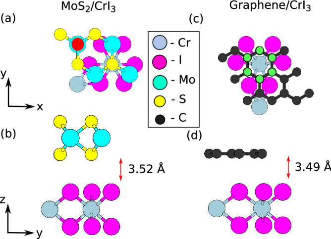
(a,b) The top and perspective view of the most stable configurations of 2:1 MoS on CrI respectively. The atom marked in red is the reference Mo atom with respect to which the various configurations have been named. (c,d) represent the same for 3:1 graphene on CrI. The graphene ring with respect to which we fix the nomenclature is highlighted by the green atoms.
Electronic structure of 2:1 MS/CrI
We now discuss the electronic and magnetic properties of 2:1 MS/CrI by calculating the spin dependent density of states (DOS) and bandstructure. We further introduce spin-orbit coupling to understand its influence on the electronic structure of the chosen heterostructure.
Figure 2a (Left panel) shows the spin-dependent DOS of pristine monolayer CrI and the system wavefunctions projected on individual atom types (Cr and I). A centered k-grid of and a Gaussian smearing of 0.004 eV has been used to visualize the DOS. The right panel of Fig. 2a shows the spin-dependent bandstructure of monolayer CrI along the k-path -K-M- spanning the first irreducible Brillouin zone. CrI is an indirect bandgap ferromagnetic semiconductor61 with a spin up bandgap of 1.24 eV and 2.11 eV for the spin-down states which is in agreement with other theoretical61 and experimental studies62. The bandgaps calculated using GGA+U method for the spin up and spin down states are 1.02 eV and 3.3 eV respectively which are in close agreement with reported values34,63. The bandgap value calculated using HSE06 is 2.12 eV52 and these values are compared and tabulated in Table 2 of SI57. The magnetic moment of Cr is 3 /atom and that of I is 0.06 /atom, which is consistent with the saturation magnetization of bulk CrI64. It is worth noting that spin-dependent nature of the bandgap for pristine CrI with the spin-up states close to the Fermi level have equal contributions from both Cr and I.
Figure 2.

Spin-polarized projected density of states (DOS) and bandstructure for (a) pristine monolayer of CrI (b) pristine (unstrained) monolayer of MoS (c) 2:1 MS/CrI (Hollow configuration) with MoS adsorbed on CrI. Gaussian smearing of 0.004 eV has been used to visualize the DOS.
The spin dependent DOS and bandstructure for unstrained MoS is shown in Fig. 2b. Pristine MoS is non-magnetic with a direct bandgap of 1.77 eV which is in good agreement with experimental65 and theoretical66 studies. Adsorption of MoS on CrI induces a strain of 7% on both the layers and has been uniformly distributed when constructing the supercell. The bandgap of monolayer strained MoS is found to exhibit a direct to indirect bandgap transition and the quantitative value of the bandgap is found to reduce with increasing values of uniaxial strain67. This is due to the phonon softening with increased strain which breaks the degeneracy of the E’ Raman modes of strained monolayer MoS67. Due to the weak van der Waals interaction at the interface of CrI and MoS, we observe a similar transition of MoS bands as seen in Fig. 2c.
In Fig. 2c, we have shown the total spin-dependent DOS, its projections on individual atom types (left panel) and bandstructure of 2:1 MS/CrI system for both its spin states (right panel). It can be observed from the DOS that the heterostructure remains magnetic with the magnetic moment largely localized on CrI. The magnetic moment on CrI remains relatively unchanged (with respect to its pristine counterpart) with 3 /atom on Cr and 0.06 /atom on I. This points to a weak van der Waals interaction between the interface inhibiting interlayer magnetic exchange. Mo and S have very negligible magnetization displaying atomic magnetic moments of 0.0005 /atom and 0.0004 /atom respectively. From the DOS shown in Fig. 2c, one can observe that the bandgap of the system reduces significantly (when compared to their pristine counterparts) to 0.53 eV for both the spin-up ad spin-down states. Above the Fermi level, the states of Mo primarily shift closer to the Fermi level and the states of Cr and I remain at relatively unchanged energies (between 0 and 1 eV). One can also observe a broadening of these states suggesting a weak interlayer hybridization. Below the Fermi level, we observe a relatively strong mixing of atomic states and a collective shift of these states closer to the Fermi level.
The electronic transition of a reduced indirect bandgap of 0.53 eV for both the spin-up and spin-down states as seen in the bandstructure of Fig. 2c can be attributed to two primary reasons: The presence of a strained MoS and the weak interlayer interaction with CrI. The bandgap values calculated using GGA+U are found to be similar with GGA approximations as tabulated in Table 2 of SI57. This can be further confirmed by performing Löwdin population analysis68 to quantify the interfacial charge transfer. It is found that MoS loses a negligible atomic charge of 0.051 electrons and CrI gains a similar value of electronic charge of 0.058 electrons. The detailed orbital projected DOS for 2:1 MS/CrI has been included in the SI57.
In Fig. 3, we show the k-resolved DOS projected onto the atomic states and this is particularly useful when the overlap and mixing of the states are high. In Fig. 3a,c,e,g we have plotted the spin resolved bands projected on Mo, S, Cr and I for 2:1 MS/CrI for the spin-up states respectively. The corresponding band projections on the spin-down states are shown in Fig. 3b,d,f,h respectively. The color scale has been normalized with respect to the maximum weight of an atomic state summed across the k-points of the Brillouin zone. The bands projected on atoms for the heterostructure system ideally shows the contribution of atom states (spin-up and down states) towards the total spin-polarized band structure shown in Fig. 2.
Figure 3.
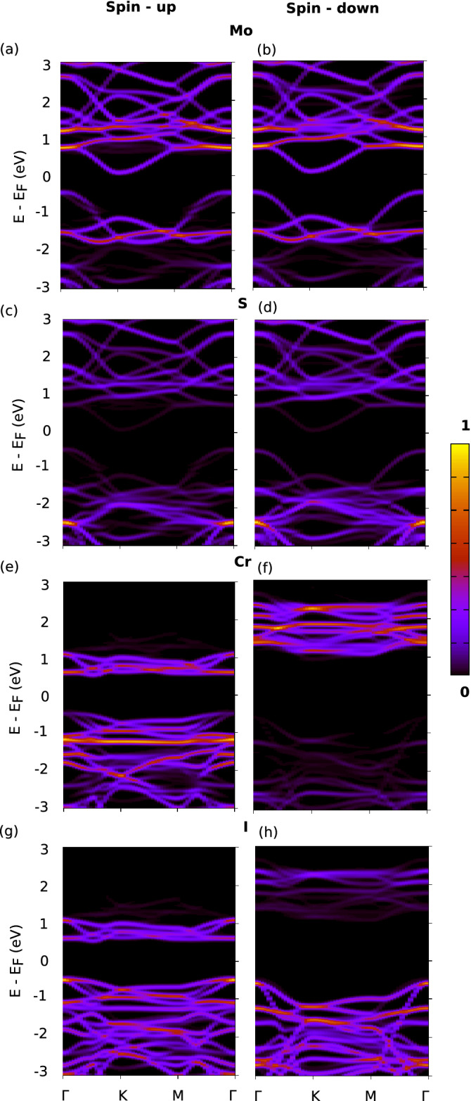
The k-resolved DOS projected on individual atom types (KDOS(k,E)) refer to “Simulation methods” section for details) is shown for (a,b) The spin up and spin down bands for 2:1 MS/CrI projected on Mo states respectively. (c,d) The spin up and spin down bands projected on S respectively. (e,f) The spin up and spin down bands projected on Cr respectively. (g,h) The spin up and spin down bands projected on I respectively. The color scale has been normalized with respect to the maximum value of the state localized around their respective atom type.
Figure 3a–d shows the KDOS projected on the spin up and spin down states of Mo and S respectively. One observes that Mo primarily contributes to the states above the Fermi level which weakly hybridize with CrI below. It is also clear that MoS remains non-magnetic upon adsoprtion. The feature regarding the reduced indirect bandgap of strained MoS is mainly due to the shift of Mo states closer to the Fermi level. This complements the results found and highlighted in the DOS projected on atoms (Fig. 2c). In Fig. 3e–h, the KDOS projected on the spin-up and spin-down states of Cr and I are shown respectively. The spin-up states just above the Fermi level (0–1 eV) show strongly hybridized Cr and I contributions and these states weakly hybridize with the Mo states of strained MoS. The spin-down states of MoS typically lie in the spin-down bandgap of CrI and remain non-interacting. This reconfirms that the strain of MoS lattice to accommodate the symmetry of CrI below and the weak interaction of the heterostructure results in the decreased spin-independent indirect bandgap for the resulting heterostructure.
The primary conclusion from examining the electronic structure of 2:1 MS/CrI would be the presence of a spin independent bandgap obtained for a ferromagnetic 2-D semiconductor. This, to our knowledge, has not been reported previously69,70. A phenomenological application of this system is realized in spin-resolved magnetic storage devices71, where the operating voltage across the two spin states would remain the same. This effect is further complemented by two aspects of this heterostructure: First is the reduced indirect band gap of 0.53 eV72 and second is its 2-D geometry which would allow higher density of spacial packing.
Electronic structure of 3:1 graphene/CrI
In this section we discuss the spin dependent electronic and magnetic properties of graphene adsorbed on monolayer of CrI. The stable configuration of this system is when the top-left graphene ring is on top of a Cr atom below and the subsequent electronic properties are studied for this configuration (3:1 G/CrI).
Figure 4a shows the spin-dependent DOS projected on individual atom types and bandstructure of pristine monolayer CrI. This has been discussed in the previous (“Electronic structure of 2:1 MS/CrI3” section) and included here for analytical completion of 3:1 G/CrI system. In Fig. 4b, we present the spin-dependent bandstructure and DOS of monolayer graphene73. It displays a non-magnetic behaviour74, exhibits no bandgap, and has a Dirac cone at K point of the Brillouin zone sampled across -K-M-75. When the periodicity of graphene is extended to a supercell within an ab initio platform using a plane wave basis set76, we find that the Dirac cone ( and ) bands exactly crosses at point due to an empirical 3N rule77.
Figure 4.

Spin-polarized projected density of states (DOS) and bandstructure for (a) pristine monolayer CrI with unit cell (b) pristine monolayer graphene with unit cell (c) 3:1 G/CrI (top configuration) with graphene adsorbed on CrI. Total DOS (grey) is magnified 2.5 times and DOS of C(dashed green) is magnified 5 times and Gaussian smearing of 0.004 eV has been used to visualize the DOS.
In Fig. 4c, we show the spin-polarized DOS and bandstructure of graphene adsorbed on CrI (3:1 G/CrI). The resulting heterostructure is found to be metallic and magnetic with the magnetic moments primarily localized on CrI52. The atomic magnetic moment of Cr is 3.07 /atom, I is 0.07575 /atom and graphene only becomes slightly magnetic with atomic magnetic moment as 0.0002 /atom. The spin-up states of CrI shift closer to the Fermi level and the Dirac cone of graphene shifts above the Fermi level. The detailed spin-resolved bands calculated with the GGA+U approximations for CrI, 2:1 MS/CrI and 3:1 G/CrI are plotted in Fig. 2 of SI57. This can be explained by Löwdin population analysis68 which quantify the interfacial charge transfer. From the Löwdin population analysis we find that graphene loses an atomic charge of 0.24 electrons and CrI gains an atomic charge of 0.24 electrons which is consistent with the shift in the electronic states as seen in Fig. 4c.
The I states are fully occupied and the Cr 3d states indicate why the heterostructure system is magnetic. But the orbitals of graphene remain unoccupied. To compensate electrons for the unoccupied orbitals of C atoms, all the spin-up and down states of Cr and I tend to move closer to the Fermi energy level where the deficient orbitals of C atoms exist. We can understand this further by comparing the C atomic states of pristine monolayer graphene and graphene states of 3:1 G/CrI. We find that the Dirac cone for the heterostructure system shifted away from the Fermi energy level by 0.075 eV. Similarly, we compared the Cr and I states of pristine CrI with its counterpart of the heterostructure system. We found that the states of Cr (3:1 G/CrI) shift towards the Fermi energy level by 0.45 eV for the states above the Fermi level. The Cr states below the Fermi level shift away from the Fermi energy level by 0.35 eV. In case of I atoms, the highest unoccupied energy levels shift towards the Fermi energy level by 0.45 eV and for the lowest occupied energy levels they shift away from the Fermi energy level by 0.26 eV. The d orbitals of Cr and p orbitals of I interact strongly with the orbitals of C atoms of graphene thereby modifying the Dirac cone of graphene only for the spin-up states for the heterostructure system. For the spin-down case, the Dirac cone falls in the band gap of the system and remains non-interacting. This suggests that there are no quantum anomalous hall (QAH) states78 present for this system in its pristine form.
In Fig. 5, we show the spin resolved bands projected in the atomic orbitals centered around the Löwdin functions for 3:1 G/CrI. The spin up and spin down bands of the system projected on the atomic orbitals of Cr have been shown in Fig. 5a,b respectively. The projections of the spin up and spin down bands on I are shown in Fig. 5c,d respectively and the same on graphene are shown in Fig. 5e,f respectively. Comparing Fig. 5a,c, it is clear that the spin up states close to the Fermi level is strongly hybridized with similar contributions from both Cr and I. The spin down states for both Cr and I lie well above the Fermi level and one would expect the interaction of graphene, close to the Fermi level, is with the spin up states of Cr and I. Although graphene remains relatively non-magnetic (pointing to a weak van der Waals’ interaction between the interfaces), the Dirac cone of the spin up states of graphene hybridize with the states of CrI. The spin-down Dirac cone is in the spin-down bandgap of CrI and does not show any hybridization. Thus we can conclude that graphene adsorbed CrI behaves as a ferromagnetic metal with graphene showing nascent Chern insulating properties. The two primary reasons for this is the interfacial charge transfer and the hybridization of graphene with the spin-up states of CrI.
Figure 5.
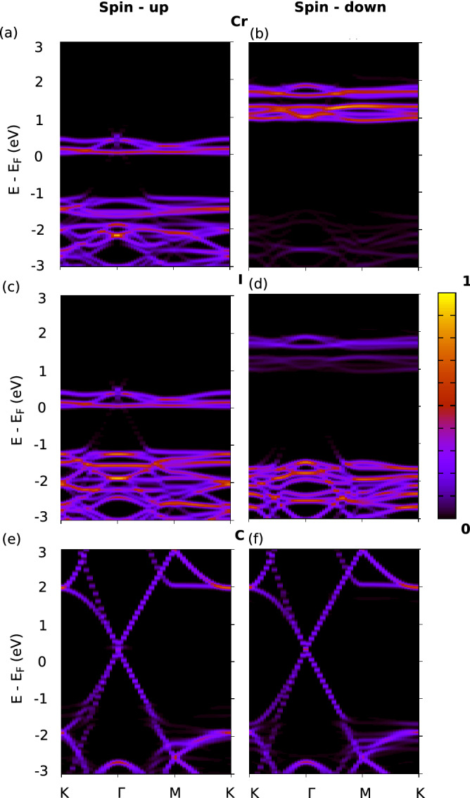
The k-resolved DOS projected on individual atom types (KDOS(k,E)) is shown for (a,b) The spin up and spin down bands for 3:1 G/CrI projected on Cr states respectively. (c,d) The spin up and spin down bands projected on I respectively. (e,f) The spin up and spin down bands projected on graphene respectively. The color scale has been normalized with respect to the maximum value of the state localized around their respective atom type.
Figure 6a shows the influence of Rashba spin-orbit coupling on the electronic properties of 2:1 MS/CrI and Fig. 6b shows the same for G/CrI heterostructure. It is observed in Fig. 6a that although the system remains an indirect bandgap semiconductor, the bandgap reduces to 0.47 eV. MoS is found to show a large energy level splitting in the presence of SOC due to matrix element effects79–81 in the order of 170 ± 2 meV corresponding to the valence band at K82. Since we consider a strained MoS weakly interacting with the substrate, the presence of SOC induces a band split of 0.01 eV corresponding to the valence band at the K point. The reduction in the bandsplitting is due to the strained MoS and substrate effects83. The conduction band energy level split corresponding to the K point is found to be 2 meV which is in agreement with other theoretical studies83. Comparing the spin-polarized bands of Fig. 3a,b with SOC bandstructure Fig. 6a, we find the valence bands shift closer by 0.29 eV towards the Fermi energy level and the conduction bands shift away by 0.23 eV from the Fermi energy level.
Figure 6.

Spin-orbit coupled (SOC) bandstructure of (a) 2:1 MS/CrI (b) 3:1 G/CrI heterostructures.
SOC plays a pivotal role in splitting energy levels of the 3:1 G/CrI heterostructure system as shown in Fig. 6b. The unoccupied conduction states of CrI shift to higher energies by 0.57 eV and graphene decouples from the substrate. The occupied SOC induced valence states of CrI shift to higher energies by a value 0.63 eV. Also these states split by an energy difference of 0.08 eV at the K point. The Dirac cone splits by 30 meV suggesting the possibility of SOC induced Chern insulating states84. Also the Dirac cone shifts up by 0.13 eV towards higher energy levels of unoccupied states.
We can therefore infer that the electronic structure of 3:1 G/CrI undergoes a transition to a ferromagnetic metal upon adsorption. We find that in the presence of spin-orbit coupling, the Dirac cone falls in the bandgap of CrI and the states begin to split. This indicates the existence of Chern insulator states which can be exaggerated by dopants or external dynamic effects52. This would play an important role in the design of spintronic devices with robust control over the spin-polarized electronic currents85.
Conclusion
We have studied the spin-dependent electronic and magnetic properties of graphene and MoS adsorbed on monolayer CrI. We find that when MoS is adsorbed on CrI, the resulting heterostructure behaves like a ferromagnetic semiconductor with a significantly reduced spin-independent, indirect bandgap of 0.53 eV. The reason for the reduced bandgap ( 70%) can be attributed to the presence of strained crystal symmetry of mono-layer MoS when grown on CrI and the weak interfacial van der Waals interactions. We attribute the reduction in the bandgap ( 70%) to the presence of strained crystal symmetry of mono-layer MoS when grown on CrI and the weak interfacial van der Waals interactions. Graphene adsorbed on CrI on the other hand was found to behave as a ferromagnetic metal and displays a significant interfacial charge transfer resulting in the shift of the graphene Dirac cone above the Fermi level. Introducing SOC for MoS/CrI results in further decrease of the indirect bandgap of the system from 0.53 to 0.47 eV. The band splitting of the conduction band Mo states (strained) was found to be 2 meV. Introducing SOC to graphene/CrI heterostructure results in the emergence of Chern insulating states with the Dirac cone splitting by 30 meV. The decoupling of the Dirac cone and the shift of the unoccupied CrI states is due to the interfacial charge transfer. These heterostructures can be used to design novel spintronic devices with efficient control over the spin channels.
Supplementary Information
Acknowledgements
This project received funding from the Science and Engineering Research Board (SERB), (Grant ID: SRG/2019/000175), Government of India under the Early Career Research grant and the authors are grateful for this.
Author contributions
S.C. performed all the numerical simulations assisted by A.R. A.R and S.C discussed the results and wrote the paper. Both the authors have reviewed the manuscript. S.C. performed all the numerical simulations assisted by A.R. A.R and S.C discussed the results and wrote the paper. Both the authors have reviewed the manuscript.
Competing interests
The authors declare no competing interests.
Footnotes
Publisher's note
Springer Nature remains neutral with regard to jurisdictional claims in published maps and institutional affiliations.
Supplementary Information
The online version contains supplementary material availlable at 10.1038/s41598-020-80290-5.
References
- 1.Lee PA, Nagaosa N, Wen X-G. Doping a Mott insulator: Physics of high-temperature superconductivity. Rev. Mod. Phys. 2006;78:17–85. doi: 10.1103/RevModPhys.78.17. [DOI] [Google Scholar]
- 2.Mermin ND, Wagner H. Absence of ferromagnetism or antiferromagnetism in one- or two-dimensional isotropic Heisenberg models. Phys. Rev. Lett. 1966;17:1133–1136. doi: 10.1103/PhysRevLett.17.1133. [DOI] [Google Scholar]
- 3.Hartmann P, Donko Z, Bakshi PM, Kalman GJ, Kyrkos S. Molecular dynamics studies of solid–liquid phase transition in 2-D yukawa systems. IEEE Trans. Plasma Sci. 2007;35:332–336. doi: 10.1109/TPS.2007.894438. [DOI] [Google Scholar]
- 4.Hellman F, et al. Interface-induced phenomena in magnetism. Rev. Mod. Phys. 2017;89:025006. doi: 10.1103/RevModPhys.89.025006. [DOI] [PMC free article] [PubMed] [Google Scholar]
- 5.Elmers H, Gradmann J. Critical behavior of the uniaxial ferromagnetic monolayer Fe(110) on W(110) Phys. Rev. B. 1996;54:15224–15233. doi: 10.1103/physrevb.54.15224. [DOI] [PubMed] [Google Scholar]
- 6.Park J-G. Opportunities and challenges of 2D magnetic van der Waals materials: Magnetic graphene? J. Phys. Condens. Matter. 2016;28:301001. doi: 10.1088/0953-8984/28/30/301001. [DOI] [PubMed] [Google Scholar]
- 7.Roldán R, Castellanos-Gomez A, Cappelluti E, Guinea F. Strain engineering in semiconducting two-dimensional crystals. J. Phys. Condens. Matter. 2015;27:313201. doi: 10.1088/0953-8984/27/31/313201. [DOI] [PubMed] [Google Scholar]
- 8.Zhong D, et al. Van der Waals engineering of ferromagnetic semiconductor heterostructures for spin and valleytronics. Sci. Adv. 2017;3:e1603113. doi: 10.1126/sciadv.1603113. [DOI] [PMC free article] [PubMed] [Google Scholar]
- 9.Cao Y, et al. Unconventional superconductivity in magic-angle graphene superlattices. Nature. 2018;556:43–50. doi: 10.1038/nature26160. [DOI] [PubMed] [Google Scholar]
- 10.Buscema M, et al. Photocurrent generation with two-dimensional van der Waals semiconductors. Chem. Soc. Rev. 2015;44:3691–3718. doi: 10.1039/C5CS00106D. [DOI] [PubMed] [Google Scholar]
- 11.Gong C, et al. Discovery of intrinsic ferromagnetism in two-dimensional van der Waals crystals. Nature. 2017;546:265–269. doi: 10.1038/nature22060. [DOI] [PubMed] [Google Scholar]
- 12.Huang B, et al. Layer-dependent ferromagnetism in a van der Waals crystal down to the monolayer limit. Nature. 2017;546:270–273. doi: 10.1038/nature22391. [DOI] [PubMed] [Google Scholar]
- 13.Gong C, Zhang X. Two-dimensional magnetic crystals and emergent heterostructure devices. Science. 2019;363:eaav4450. doi: 10.1126/science.aav4450. [DOI] [PubMed] [Google Scholar]
- 14.Lee J-U, et al. Ising-type magnetic ordering in atomically thin FePS3. Nano Lett. 2016;16:7433–7438. doi: 10.1021/acs.nanolett.6b03052. [DOI] [PubMed] [Google Scholar]
- 15.Wang X, et al. Raman spectroscopy of atomically thin two-dimensional magnetic iron phosphorus trisulfide (FePS3) crystals. TDM. 2016;3:031009. doi: 10.1088/2053-1583/3/3/031009. [DOI] [Google Scholar]
- 16.Bonilla M, et al. Strong room-temperature ferromagnetism in VSe2 monolayers on van der Waals substrates. Nat. Nanotechnol. 2018;13:289–293. doi: 10.1038/s41565-018-0063-9. [DOI] [PubMed] [Google Scholar]
- 17.O’Hara D, et al. Room temperature intrinsic ferromagnetism in epitaxial manganese selenide films in the monolayer limit. Nano Lett. 2018;18:3125–3131. doi: 10.1021/acs.nanolett.8b00683. [DOI] [PubMed] [Google Scholar]
- 18.Geim AK, Novoselov KS. The rise of graphene. Nat. Mater. 2007;6:183–191. doi: 10.1038/nmat1849. [DOI] [PubMed] [Google Scholar]
- 19.Sichau J, et al. Resonance microwave measurements of an intrinsic spin–orbit coupling gap in graphene: A possible indication of a topological state. Phys. Rev. Lett. 2019;122:046403. doi: 10.1103/PhysRevLett.122.046403. [DOI] [PubMed] [Google Scholar]
- 20.Bubnova O. Do-it-yourself thermoelectrics. Nat. Nanotechnol. 2019;14:194. doi: 10.1038/s41565-019-0411-4. [DOI] [Google Scholar]
- 21.Mak KF, Lee C, Hone J, Shan J, Heinz TF. Atomically thin : A new direct-gap semiconductor. Phys. Rev. Lett. 2010;105:136805. doi: 10.1103/PhysRevLett.105.136805. [DOI] [PubMed] [Google Scholar]
- 22.Chhowalla M, et al. The chemistry of two-dimensional layered transition metal dichalcogenide nanosheets. Nat. Chem. 2013;5:263–275. doi: 10.1038/nchem.1589. [DOI] [PubMed] [Google Scholar]
- 23.He Y, et al. Self-assembly of block copolymers into sieve-like particles with arrayed switchable channels and as scaffolds to guide the arrangement of gold nanoparticles. Nanoscale. 2017;9:15056–15061. doi: 10.1039/C7NR04923D. [DOI] [PubMed] [Google Scholar]
- 24.Duan J, et al. Solid-state batteries: Lithium–graphite paste: An interface compatible anode for solid-state batteries. Adv. Mater. 2019;31:1970068. doi: 10.1002/adma.201970068. [DOI] [PubMed] [Google Scholar]
- 25.Götte M, Joppe M, Dahm T. Pure spin current devices based on ferromagnetic topological insulators. Sci. Rep. 2016;6:1–9. doi: 10.1038/srep36070. [DOI] [PMC free article] [PubMed] [Google Scholar]
- 26.Qi X-L, Zhang S-C. Topological insulators and superconductors. Rev. Mod. Phys. 2011;83:1057–1110. doi: 10.1103/RevModPhys.83.1057. [DOI] [Google Scholar]
- 27.Fu L, Kane CL. Superconducting proximity effect and majorana fermions at the surface of a topological insulator. Phys. Rev. Lett. 2008;100:096407. doi: 10.1103/PhysRevLett.100.096407. [DOI] [PubMed] [Google Scholar]
- 28.Zak J, Moog ER, Liu C, Bader SD. Universal approach to magneto-optics. JMMM. 1990;89:107–123. doi: 10.1016/0304-8853(90)90713-Z. [DOI] [Google Scholar]
- 29.Arnold DP. Review of microscale magnetic power generation. IEEE Trans. Mag. 2007;43(11):3940–3951. doi: 10.1109/TMAG.2007.906150. [DOI] [Google Scholar]
- 30.Huang B, et al. Electrical control of 2D magnetism in bilayer CrI 3. Nat. Nanotechnol. 2018;13:544–548. doi: 10.1038/s41565-018-0121-3. [DOI] [PubMed] [Google Scholar]
- 31.Samarth N. Condensed-matter physics: Magnetism in flatland. Nature. 2017;546:216–218. doi: 10.1038/546216a. [DOI] [PubMed] [Google Scholar]
- 32.Lado, J.L. & Fernández-Rossier, J. On the origin of magnetic anisotropy in two dimensional CrI. arXiv10.1088/2053-1583/aa75ed(2017). eprint 1704.03849.
- 33.Burch KS, Mandrus D, Park J-G. Magnetism in two-dimensional van der Waals materials. Nature. 2018;563:47–52. doi: 10.1038/s41586-018-0631-z. [DOI] [PubMed] [Google Scholar]
- 34.Chen S, et al. Boosting the curie temperature of two-dimensional semiconducting CrI3 monolayer through van der Waals heterostructures. J. Phys. Chem. C. 2019;123:17987–17993. doi: 10.1021/acs.jpcc.9b04631. [DOI] [Google Scholar]
- 35.Tannous C, Comstock RL. Magnetic information-storage materials. SpringerLink. 2017 doi: 10.1007/978-3-319-48933-9_49. [DOI] [Google Scholar]
- 36.Patel K, Zhang J, Ren S. Rare-earth-free high energy product manganese-based magnetic materials. Nanoscale. 2018;10:11701–11718. doi: 10.1039/C8NR01847B. [DOI] [PubMed] [Google Scholar]
- 37.Ambashta RD, Sillanpää M. Water purification using magnetic assistance: a review. J. Hazard. Mater. 2010;180:38–49. doi: 10.1016/j.jhazmat.2010.04.105. [DOI] [PubMed] [Google Scholar]
- 38.Cortie MB, Cortie DL, Timchenko V. Heat transfer from nanoparticles for targeted destruction of infectious organisms. Int. J. Hyperthermia. 2018;34:157–167. doi: 10.1080/02656736.2017.1410236. [DOI] [PubMed] [Google Scholar]
- 39.Parkin SSP, et al. Giant tunnelling magnetoresistance at room temperature with MgO (100) tunnel barriers. Nat. Mater. 2004;3:862–867. doi: 10.1038/nmat1256. [DOI] [PubMed] [Google Scholar]
- 40.Yuasa S, Nagahama T, Fukushima A, Suzuki Y, Ando K. Giant room-temperature magnetoresistance in single-crystal Fe/MgO/Fe magnetic tunnel junctions. Nat. Mater. 2004;3:868–871. doi: 10.1038/nmat1257. [DOI] [PubMed] [Google Scholar]
- 41.Moodera JS, Kinder LR, Wong TM, Meservey R. Large magnetoresistance at room temperature in ferromagnetic thin film tunnel junctions. Phys. Rev. Lett. 1995;74:3273–3276. doi: 10.1103/PhysRevLett.74.3273. [DOI] [PubMed] [Google Scholar]
- 42.Ghazaryan D, et al. Magnon-assisted tunnelling in van der Waals heterostructures based on CrBr 3. Nat. Electron. 2018;1:344–349. doi: 10.1038/s41928-018-0087-z. [DOI] [Google Scholar]
- 43.Jiang, S., Li, L., Wang, Z., Shan, J. & Mak, K.F. Spin transistor built on 2D van der Waals heterostructures. arXiv (2018). Eprint 1807.04898.
- 44.Dushenko S, et al. Gate-tunable spin-charge conversion and the role of spin–orbit interaction in graphene. Phys. Rev. Lett. 2016;116:166102. doi: 10.1103/PhysRevLett.116.166102. [DOI] [PubMed] [Google Scholar]
- 45.Rassekh M, He J, Farjami Shayesteh S, Palacios JJ. Remarkably enhanced Curie temperature in monolayer CrI3 by hydrogen and oxygen adsorption: A first-principles calculations. Comput. Mater. Sci. 2020;183:109820. doi: 10.1016/j.commatsci.2020.109820. [DOI] [Google Scholar]
- 46.Guo Y, Yuan S, Wang B, Shi L, Wang J. Half-metallicity and enhanced ferromagnetism in Li-adsorbed ultrathin chromium triiodide. J. Mater. Chem. C. 2018;6:5716–5720. doi: 10.1039/C8TC01302K. [DOI] [Google Scholar]
- 47.Zhong D, et al. Layer-resolved magnetic proximity effect in van der Waals heterostructures. Nat. Nanotechnol. 2020;15:1–5. doi: 10.1038/s41565-019-0629-1. [DOI] [PubMed] [Google Scholar]
- 48.van Setten MJ. Electronic structure and formation enthalpy of hydroaluminates and hydroborates. Encycl. Mater. Sci. Technol. 2008 doi: 10.1016/B978-008043152-9.02192-8. [DOI] [Google Scholar]
- 49.Perdew JP, Burke K, Ernzerhof M. Generalized gradient approximation made simple. Phys. Rev. Lett. 1996;77:3865–3868. doi: 10.1103/PhysRevLett.77.3865. [DOI] [PubMed] [Google Scholar]
- 50.Giannozzi P, et al. QUANTUM ESPRESSO: A modular and open-source software project for quantum simulations of materials. J. Phys. Condens. Matter. 2009;21:395502. doi: 10.1088/0953-8984/21/39/395502. [DOI] [PubMed] [Google Scholar]
- 51.Monkhorst HJ, Pack JD. Special points for Brillouin-zone integrations. Phys. Rev. B. 1976;13:5188–5192. doi: 10.1103/PhysRevB.13.5188. [DOI] [Google Scholar]
- 52.Zhang J, et al. Strong magnetization and Chern insulators in compressed graphene/CrI3 van der Waals heterostructures. Phys. Rev. B. 2018;97:085401. doi: 10.1103/PhysRevB.97.085401. [DOI] [Google Scholar]
- 53.Grimme S. Semiempirical GGA-type density functional constructed with a long-range dispersion correction. J. Comput. Chem. 2006;27:1787–1799. doi: 10.1002/jcc.20495. [DOI] [PubMed] [Google Scholar]
- 54.Tolba, S.A., Gameel, K.M., Ali, B.A., Hossam, A. & Allam, N.K. The DFT+U: Approaches, accuracy, and applications. In Density Functional Calculations—Recent Progresses of Theory and Application. 10.5772/intechopen.72020(IntechOpen, 2018).
- 55.Pela RR, Marques M, Teles LK. Comparing LDA-1/2, HSE03, HSE06 and G0W0 approaches for band gap calculations of alloys. J. Phys. Condens. Matter. 2015;27:505502. doi: 10.1088/0953-8984/27/50/505502. [DOI] [PubMed] [Google Scholar]
- 56.Dudarev SL, Botton GA, Savrasov SY, Humphreys CJ, Sutton AP. Electron-energy-loss spectra and the structural stability of nickel oxide: An LSDA+U study. Phys. Rev. B. 1998;57:1505–1509. doi: 10.1103/PhysRevB.57.1505. [DOI] [Google Scholar]
- 57.Shamik Chakraborty, A.R. Supplementary Information.
- 58.Kokalj A. XCrySDen—A new program for displaying crystalline structures and electron densities. J. Mol. Gr. Model. 1999;17:176–179. doi: 10.1016/S1093-3263(99)00028-5. [DOI] [PubMed] [Google Scholar]
- 59.Soler JM, et al. The SIESTA method for ab initio order-N materials simulation. J. Phys. Condens. Matter. 2002;14:2745–2779. doi: 10.1088/0953-8984/14/11/302. [DOI] [Google Scholar]
- 60.Yang B, Zhang X, Yang H, Han X, Yan Y. Strain controlling transport properties of heterostructure composed of monolayer CrI3. Appl. Phys. Lett. 2019;114:192405. doi: 10.1063/1.5091958. [DOI] [Google Scholar]
- 61.Webster L, Liang L, Yan J-A. Distinct spin–lattice and spin–phonon interactions in monolayer magnetic CrI3. Phys. Chem. Chem. Phys. 2018;20:23546–23555. doi: 10.1039/C8CP03599G. [DOI] [PubMed] [Google Scholar]
- 62.Wu M, Li Z, Cao T, Louie SG. Physical origin of giant excitonic and magneto-optical responses in two-dimensional ferromagnetic insulators. Nat. Commun. 2019;10:1–8. doi: 10.1038/s41467-019-10325-7. [DOI] [PMC free article] [PubMed] [Google Scholar]
- 63.Kuklin AV, Visotin MA, Baek W, Avramov PV. CrI3 magnetic nanotubes: A comparative DFT and DFT+U study, and strain effect. Physica E. 2020;123:114205. doi: 10.1016/j.physe.2020.114205. [DOI] [Google Scholar]
- 64.Richter N, et al. Temperature-dependent magnetic anisotropy in the layered magnetic semiconductors CrI3 and CrBr3. Phys. Rev. Mater. 2018;2:024004. doi: 10.1103/PhysRevMaterials.2.024004. [DOI] [Google Scholar]
- 65.Dolui K, Rungger I, Das Pemmaraju C, Sanvito S. Possible doping strategies for MoS monolayers: An ab initio study. Phys. Rev. B. 2013;88:075420. doi: 10.1103/PhysRevB.88.075420. [DOI] [Google Scholar]
- 66.Gusakova J, et al. Electronic properties of bulk and monolayer TMDs: Theoretical study within DFT framework (GVJ-2e method) Phys. Status Solidi A. 2017;214:1700218. doi: 10.1002/pssa.201700218. [DOI] [Google Scholar]
- 67.Conley HJ, et al. Bandgap engineering of strained monolayer and bilayer MoS2. Nano Lett. 2013;13:3626–3630. doi: 10.1021/nl4014748. [DOI] [PubMed] [Google Scholar]
- 68.Bruhn G, Davidson ER, Mayer I, Clark AE. Löwdin population analysis with and without rotational invariance. Int. J. Quantum Chem. 2006;106:2065–2072. doi: 10.1002/qua.20981. [DOI] [Google Scholar]
- 69.Anh LD, Hai PN, Tanaka M. Observation of spontaneous spin-splitting in the band structure of an n-type zinc-blende ferromagnetic semiconductor. Nat. Commun. 2016;7:1–8. doi: 10.1038/ncomms13810. [DOI] [PMC free article] [PubMed] [Google Scholar]
- 70.Zhang F, Mi W, Wang X. Spin-dependent electronic structure and magnetic anisotropy of 2D ferromagnetic Janus Cr2I3X3 (X = Br, Cl) monolayers. Adv. Electron. Mater. 2020;6:1900778. doi: 10.1002/aelm.201900778. [DOI] [Google Scholar]
- 71.Puebla J, Kim J, Kondou K, Otani Y. Spintronic devices for energy-efficient data storage and energy harvesting. Commun. Mater. 2020;1:1–9. doi: 10.1038/s43246-020-0022-5. [DOI] [Google Scholar]
- 72.Schwierz F, Granzner R, Pezoldt J. Two-dimensional materials and their prospects in transistor electronics. Nanoscale. 2015 doi: 10.1039/C5NR01052G. [DOI] [PubMed] [Google Scholar]
- 73.Fathi D. A Review of electronic band structure of graphene and carbon nanotubes using tight binding. J. Nanotechnol. 2011 doi: 10.1155/2011/471241. [DOI] [Google Scholar]
- 74.Liu Y, et al. Realization of ferromagnetic graphene oxide with high magnetization by doping graphene oxide with nitrogen. Sci. Rep. 2013;3:1–5. doi: 10.1038/srep02566. [DOI] [PMC free article] [PubMed] [Google Scholar]
- 75.Bostwick A, Ohta T, Seyller T, Horn K, Rotenberg E. Quasiparticle dynamics in graphene. Nat. Phys. 2006;3:36–40. doi: 10.1038/nphys477. [DOI] [Google Scholar]
- 76.Martínez-Duart JM, Martín-Palma RJ, Agulló-Rueda F. Nanotechnology for Microelectronics and Optoelectronics. Amsterdam: Elsevier; 2006. [Google Scholar]
- 77.Zhou Y, Zhang H-L, Deng W-Q. A 3 N rule for the electronic properties of doped graphene. Nanotechnology. 2013;24:225705. doi: 10.1088/0957-4484/24/22/225705. [DOI] [PubMed] [Google Scholar]
- 78.Liu C-X, Zhang S-C, Qi X-L. The quantum anomalous Hall effect: Theory and experiment. Annu. Rev. Condens. Matter Phys. 2016;7:301–321. doi: 10.1146/annurev-conmatphys-031115-011417. [DOI] [Google Scholar]
- 79.Bansil A, Lindroos M. Importance of matrix elements in the ARPES spectra of BISCO. Phys. Rev. Lett. 1999;83:5154–5157. doi: 10.1103/PhysRevLett.83.5154. [DOI] [Google Scholar]
- 80.Sahrakorpi S, Lindroos M, Markiewicz RS, Bansil A. Evolution of midgap states and residual three dimensionality in . Phys. Rev. Lett. 2005;95:157601. doi: 10.1103/PhysRevLett.95.157601. [DOI] [PubMed] [Google Scholar]
- 81.Bansil A, Lindroos M, Sahrakorpi S, Markiewicz RS. Influence of the third dimension of quasi-two-dimensional cuprate superconductors on angle-resolved photoemission spectra. Phys. Rev. B. 2005;71:012503. doi: 10.1103/PhysRevB.71.012503. [DOI] [Google Scholar]
- 82.Latzke DW, et al. Electronic structure, spin–orbit coupling, and interlayer interaction in bulk . Phys. Rev. B. 2015;91:235202. doi: 10.1103/PhysRevB.91.235202. [DOI] [Google Scholar]
- 83.Cheiwchanchamnangij T, Lambrecht WRL, Song Y, Dery H. Strain effects on the spin–orbit-induced band structure splittings in monolayer MoS2 and graphene. Phys. Rev. B. 2013;88:155404. doi: 10.1103/PhysRevB.88.155404. [DOI] [Google Scholar]
- 84.Qiao Z, et al. Quantum anomalous Hall effect in graphene from Rashba and exchange effects. Phys. Rev. B. 2010;82:161414. doi: 10.1103/PhysRevB.82.161414. [DOI] [Google Scholar]
- 85.Xue Y, et al. Novel Chern insulators with half-metallic edge states. NPG Asia Mater. 2018;10:e467. doi: 10.1038/am.2017.240. [DOI] [Google Scholar]
Associated Data
This section collects any data citations, data availability statements, or supplementary materials included in this article.