Abstract
A wireless and battery-less trimodal neural interface system-on-chip (SoC), capable of 16-ch neural recording, 8-ch electrical stimulation, and 16-ch optical stimulation, all integrated on a 5×3 mm2 chip fabricated in 0.35-μm standard CMOS process. The trimodal SoC is designed to be inductively powered and communicated. The downlink data telemetry utilizes on-off keying pulse-position modulation (OOK-PPM) of the power carrier to deliver configuration and control commands at 50 kbps. The analog front-end (AFE) provides adjustable mid-band gain of 55–70 dB, low/high cut-off frequencies of 1–100 Hz/10 kHz, and input-referred noise of 3.46 μVrms within 1 Hz-50 kHz band. AFE outputs of every two-channel are digitized by a 50 kS/s 10-bit SAR-ADC, and multiplexed together to form a 6.78 Mbps data stream to be sent out by OOK modulating a 434 MHz RF carrier through a power amplifier (PA) and 6 cm monopole antenna, which form the uplink data telemetry. Optical stimulation has a switched-capacitor based stimulation (SCS) architecture, which can sequentially charge 4 storage capacitor banks up to 4 V and discharge them in selected μLEDs at instantaneous current levels of up to 24.8 mA on demand. Electrical stimulation is supported by 4 independently driven stimulating sites at 5-bit controllable current levels in ±(25–775) μA range, while active/passive charge balancing circuits ensure safety. In vivo testing was conducted on 4 anesthetized rats to verify the functionality of the trimodal SoC.
Keywords: trimodal neural interface, optogenetics, switched-capacitor based stimulation, charge balancing, wireless power and data transmission
I. Introduction
A subset of implantable microelectronic devices (IMD) known as neural interfaces are aimed at establishing a direct communication pathway with the central nervous system (CNS) for understanding of brain functions and performing promising treatment of neurological disorders [1]–[3]. Deep brain stimulation (DBS) has been proven therapeutically effective for neurological disorders, such as Parkinson’s disease, epilepsy, and Alzheimer’s disease [4], [5]. DBS involves injecting a designated amount of charge into the target neural tissue to initiate the functional response of neurons in patients unresponsive to pharmaceutical treatment [6].
In addition to neuromodulation, neural interface devices are also expected to be able to sense and register neural activities with high spatiotemporal resolution [7], [8]. Analyzing neural signals helps researchers to observe and interpret the changes in neural activities in response to various stimulation patterns. The recorded data also provides feedback on the evoked neural activities to help adjust stimulation parameters/pattems to optimize them in terms of efficacy, safety, side effects, and power efficiency in what is known as closed-loop neuromodulation [7], [8]. To meet these requirements, several IMDs capable of neural recording and electrical stimulation have been developed for closed-loop neuromodulation applications [9]–[14].
A much more recent approach to neuromodulation, known as optical stimulation, has rapidly become popular among neuroscientists. It has distinct advantages over electrical stimulation, such as cell-type specificity, sub-millisecond temporal precision, rapid reversibility, and elimination of electrical artifacts, and can potentially substitute/complement traditional neuromodulation [15], [16]. Recent demand on neural interface devices for optical neuromodulation application has resulted in the development of neural interface devices offering optical stimulation capability [17]–[22]. A weakness of these devices from a translational standpoint is their high power consumption, which is inevitable because of the high threshold of light intensity, in the order of 1 mW/mm2 at 470 nm, needed to elicit selective neuromodulation. Therefore, it is hypothesized that applying a small subthreshold current during the optical stimulation could reduce the threshold of the optical stimulation, and consequently the power needed for the selective optical stimulation. Therefore, a comprehensive neural interface furnished with both optical and electrical stimulation capabilities, plus neural recording of the evoked activity for closing the loop is expected to offer unprecedented flexibility for end-users to execute sophisticated hybrid neuromodulation paradigms in a closed-loop fashion [23]–[26].
Another key feature, which brings such advanced neural interface devices closer to clinical use is wireless operation in terms of both power delivery and data transmission. The conventional communication pathway requires cable tethering between the device and the external data aggregator, which imposes several limitations for studies of freely behaving animals [27]–[29]. These limitations include potentially biased behavioral outcomes, tangling or breakage of cables during experiments, and potential discomfort and stress of the animal subjects [30]–[32]. Although battery powered IMDs are available for low power applications, such as pacemakers or DBS, they do not seem to be able to support long term optical stimulation experiments even in small animal subjects. Optical stimulation suffers from high power consumption because of the high threshold of light intensity needed to elicit selective neuromodulation, which at 470 nm is ~1 mW/mm2 [33].
In this paper, we elaborate on [26], where we reported for the first time a fully-integrated, wireless and battery-less trimodal neural interface system-on-chip (SoC) for 16-channel neural recording, 8-channel electrical stimulation, and 16-channel optical stimulation. We confirmed the functionality of the proposed trimodal SoC by demonstrating evoked neural activities and immunostained tissue response in vivo. An overview of the experimental setup for wirelessly operating the trimodal SoC is given in Section II. Section III presents a detailed design of the SoC. Section IV shows benchtop measurement results. Section V and Section VI describe the in vivo and in vitro results, respectively, followed by discussion and conclusion.
II. System Architecture
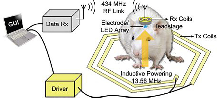
Fig. 1 shows the conceptual view of the experimental setup, including the trimodal SoC and the wireless power/data links, for performing behavioral studies on small freely moving animals, such as rodents. The SoC, together with several commercial-off-the-shelf (COTS) components (e.g. passive capacitors and inductors), receiver (Rx) coils, and a transmitter (Tx) antenna, can be incorporated in a head-mounted device, which unlike cables, will not bias the animal subject’s behavior.
Fig. 1.
Conceptual view of wirelessly operating the trimodal SoC built in a device, which is mounted on the head of a freely moving rat.
Wireless power delivery to the trimodal SoC is achieved through a multi-coil inductive link operating at 13.56 MHz. The Tx coils in this case can be a wirelessly powered rodent homecage, like the EnerCage-HC system [31], [32]. Wireless data communication with the SoC is bi-directional. The downlink data telemetry, which is achieved by modulating the amplitude of the power carrier of the inductive link, delivers configuration and control commands to the SoC. Once receiving the user-defined parameters, the SoC will generate stimulation pulses to either drive μLEDs for optical stimulation or inject current through stimulation sites for electrical stimulation, while recording evoked neural activities through a separate electrode array. For the uplink data telemetry, the recording data is digitized and transferred to the data Rx outside the homecage through a separate 434 MHz RF link.
Considering the large volume of the recorded raw data, the receiver (Data-Rx) in this case is a custom-designed data acquisition system, which incorporates multiple BladeRF software defined radios (SDRs) for complete spatial coverage without any blind spots that operate in parallel via USB links to a PC that performs real-time data recovery, processing, display, and storage [34].
III. Trimodal SoC Architecture
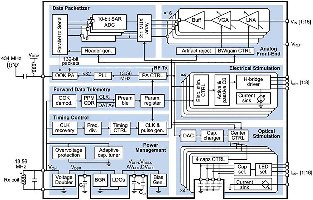
Fig. 2 shows the top-level block diagram of the WINeRS-9 SoC. The power management block generates regulated supplies (1.8 V, 3.3 V, and 4.2 V) and biasing for the rest of the SoC from the 13.56 MHz power carrier, while an adaptive capacitor tuner compensates the resonance capacitance variations. The timing control block recovers a 13.56 MHz clock from the power carrier and generates control signals to sync other blocks. The forward data telemetry block recovers adjustable parameters from the on-off-keying (OOK) modulated coil voltage, Vcoil, to configure stimulation and recording settings.
Fig. 2.
Overall block diagram of the trimodal SoC.
The SoC generates stimulation pulses based on the user-defined stimulation types and patterns. Optical stimulation employs a switched-capacitor based stimulation (SCS) architecture, which can deliver instantaneous currents large enough for the intensity of light produced by the flashing μLEDs to be large enough to surpass the optogenetic neuromodulation threshold without overloading the inductive link or creating a mismatch [35]. For electrical stimulation, an H-bridge drives stimulating sites with constant current in a biphasic-bipolar fashion, while both active and passive charge balancing (CB) circuits can be engaged to ensure the residual voltage difference across a pair of active site staying within a safe window (± 50 mV) [36], [37].
The recording function is performed by 16 analog front-end (AFE) channels, which amplify and filter recorded neural signals with the user-defined gain and bandwidth. An artifact rejection (AR) circuit is adapted to prevent the AFE from saturation during stimulation periods. Each successive approximation register (SAR) analog-to-digital converter (ADC) takes sample alternatively between two AFE channels at 50 kS/s, resulting in 25 kS/s for each channel. Each digitization cycle generates 132 data bits, which are serially sent to the RF Tx block, in which the serial data bit stream OOK modulates a 434 MHz carrier before being transmitted by the PA through a small monopole antenna. The power supply of the 434 MHz matching network is provided by one of the on-chip LDOs. Each 132-bit data package produced includes party check bit and 11-bit preamble ahead of the ADC raw data in order to improve the accuracy of packet detection on the data Rx side.
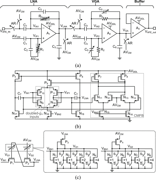
Each AFE channel includes three stages, as shown in Fig. 3a: a low noise amplifier (LNA), a variable gain amplifier (VGA), and an analog buffer. The LNA and VGA employ DC blocking capacitors, C1 and C4, at the input to remove DC offset, while their common-mode voltages are biased at half of the supply voltage, AVCM. The LNA utilizes doubled transconductance (gm) input stages to help achieve low input-referred noise [38]. The common-mode feedback (CMFB) amplifier sets the internal voltage of doubled-gm input stages to AVCM. The buffer is able to drive the large switched-capacitor array of the SAR ADC. The ‘AR’ pulse, synchronized with the stimulation pulse, detaches the AFE from the recording electrodes and connects the inputs and outputs of LNA and VGA to AVCM so that the recording function of the AFE can recover right after the stimulation pulse is over. The low cutoff frequency of the AFE is set by the LNA at l/(2π R1 C2), while the high cutoff frequency of the AFE is determined by the VGA bandwidth. The mid-band gain of the AFE is determined by the gains of the LNA and VGA, which are set by C1/C2 and C4/C5, respectively. C5 is a 3-bit binary-weighted capacitor array and adjusts the VGA gain. In Fig. 3c, R1 is implemented using a cross-coupled pseudo resistor, which prevents DC current flow through transistors, P1 and P2 [39]. This pseudo resistor and its 3-bit programmable current source sets the low cutoff frequency.
Fig. 3.
Schematic diagram of (a) a single AFE channel, (b) the amplifier, A1, and (c) the adjustable pseudo resister, R1.
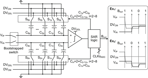
We adopted the low power and robust SAR ADC architecture in [40] and modified it for this particular application. In the sampling phase, the input signals, VIP and VIN, are sampled onto the top plates of the capacitor arrays through bootstrapped switches. In the following comparison phase, the bootstrapped switches turn off and the bottom plates of the capacitor arrays are switched between DVDDL, DVCM, and ground, where DVDDL is the digital supply voltage, and DVCM equals DVDDL/2. By taking the capacitor switching scheme in [40], the number of capacitors in this ADC is reduced by 75% over the conventional architecture in [41]. Moreover, by dramatically reducing energy consumption in the first 3 bit-cycles and reducing the switching step of each capacitor by half, power saving can be achieved.
In Fig. 4, the comparator input waveforms resulted from the switching scheme in [40] show that if ‘1’ is generated after the second bit cycle, the comparator input will successively approach to DVCM in the following bit cycles; otherwise, the comparator input will successively deviate from DVCM. However, thanks to the halved switching step, the comparator input derivation from DVCM is still less than that in the monotonic switching scheme in [41].
Fig. 4.
Schematic diagram of the 10-bit SAR ADC, with two examples of the comparator input waveforms.
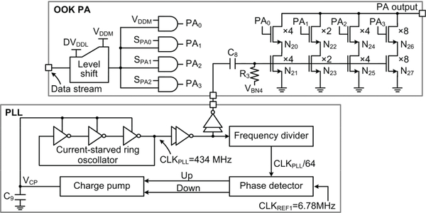
As shown in Fig. 5, the RF Tx mainly consists of a phase-locked loop (PLL) and OOK PA [42]. In the PLL block, the clock, CLKPLL, generated by a 3-stage ring oscillator is divided by 64. The phase detector compares the divided clock with a 6.78 MHz reference clock, CLKREF1, which is derived from the 13.56 MHz clock. The charge pump charges/discharges the capacitor, C9, to control the bias voltage of the ring oscillator, VCP, based on the ‘Up/Down’ output pulses from the phase detector. When the loop is stabilized, CLKPLL becomes 64×CLKREF1=434 MHz, which is buffered to drive the PA. The output power of the OOK PA is 3-bit adjustable. The data bit stream is serially sent out by OOK modulating the PA carrier at 6.78 Mbps.
Fig. 5.
Schematic diagram of the RF Tx, including PLL and OOK PA.
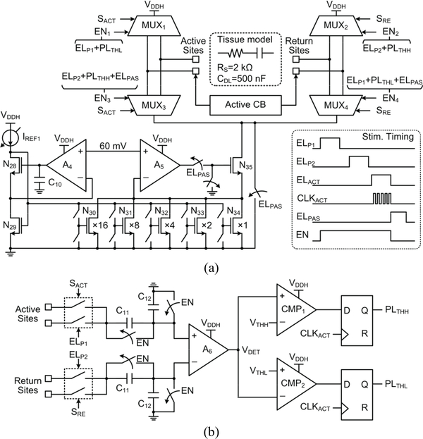
The electrical stimulation block includes four independent groups, one of which is shown in Fig. 6a. A current stimulator employs four 4:1 multiplexers (MUXs) in an H-bridge configuration, which interface with two active and two return sites. A controller selects the MUXs in pairs to generate anodic and cathodic stimulation phases with a single current driver, which consists of a 5-bit current steering digital-to-analog converter (DAC), implemented with low dropout transistors [43]. The feedback loops, using amplifiers A4 and A5, set the drain-source voltages of N30-N34 transistors at 60 mV in the triode region to reduce the voltage headroom of the current driver output, while boosting its output impedance [37]. As shown in Fig. 6b, the active CB circuit monitors the voltage difference between the active and return stimulating sites selected by control signals, SACT and SRE, during the stimulation and active CB periods, when EN = 1. When the stimulation starts, EN = ‘1’, the site voltage difference is capacitively attenuated before being converted to a single-ended output voltage, VDET. If the site voltage difference goes above a ±50 mV window, VDET will exceed the bounds set by VTHH and VTHL. In response, a sequence of pulses, either PLTHH or PLTHL will be generated to control the four MUXs, which will push or pull additional current pulses into the tissue to keep the sites’ voltage difference within the safe window. After the active CB period, the passive CB circuit is then activated to further remove the residual charge by shorting the two stimulating sites to ground.
Fig. 6.
Schematic diagram of (a) a single group in the electrical stimulation block and (b) the active CB circuit.
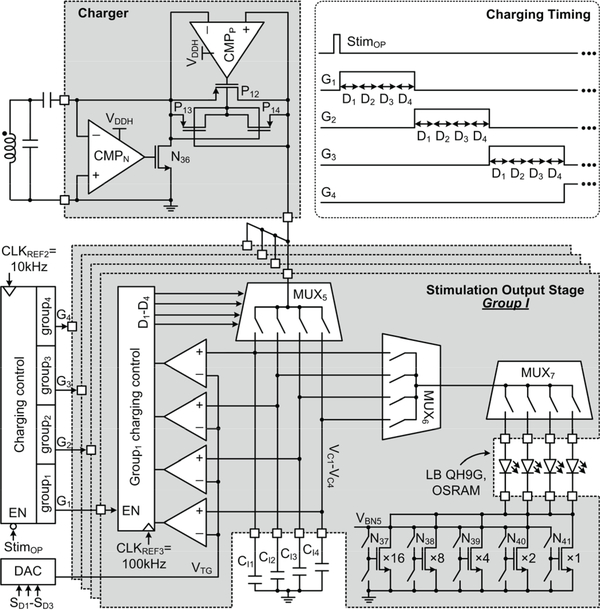
Fig. 7 shows a simplified schematic diagram of the optical stimulation block, which utilizes the SCS architecture [35]. The capacitor charger consists of two switches driven by two high-speed comparators, CMPN and CMPP, sequentially charging four off-chip capacitor banks during their corresponding charging periods, G1-G4, which are adjustable by the charging control circuit. The charging cycle continues until the next stimulation flag signal, StimOP, arrives. Each capacitor bank includes four surface-mount (SMD) capacitors. In each group, the charging control circuit adjusts the charging periods, D1-D4, for the 4 capacitors, CI1-CI4, to be charged in sequence to a target voltage, VTG, set by a 3-bit DAC, through MUX5. MUX6 controls which capacitor(s) of CI1-CI4 to dump their charge into one of the 4 μLEDs, decided by the MUX7, for performing optical stimulation with adjustable pulse width and frequency. A current limiter, implemented using a 5-bit current sink with binary-weighted transistors, sets an upper bound to the exponentially decaying current that flows through the μLED.
Fig. 7.
Schematic diagram of the optical stimulation block.
IV. Measurement Results
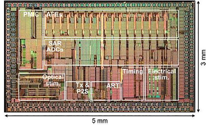
The die photo of the trimodal SoC, shown in Fig. 8, was fabricated in the TSMC 0.35-μm 4M2P standard CMOS process and occupies 5×3 mm2 of silicon area including pads.
Fig. 8.
The fabricated trimodal SoC micrograph.
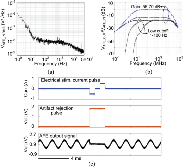
Fig. 9a presents the measured AFE input-referred noise spectrum. The thermal noise level is observed at 10 nV/√Hz and 1/f noise corner occurs at 20 Hz. Integration under this curve from 1 Hz to 50 kHz yields a root mean square (RMS) noise voltage of 3.46 μVrms for the AFE, with a noise efficiency factor (NEF) of 2.95 [38]. Fig. 9b presents the measured frequency response of the AFE. The low cutoff frequency of the AFE is adjustable from 1–100 Hz, while the gain of the AFE is changed from 55–70 dB. The high cutoff frequency of the AFE, determined by the VGA bandwidth, is at 10 kHz. Fig. 9c shows measured waveforms of electrical stimulation and stimulus artifact rejection. The SoC injects a series of ±500 μA current pulses into a tissue model consisting of RS = 2 kΩ and CDL = 500 nF connected in series [37], while amplifying and filtering a 1 mVpp, 600 Hz sinusoidal input. When the stimulation starts, ‘AR’ signal is generated to force the AFE output staying at 0.9 V and to recover the recording function in 0.4 ms after the stimulation, protecting the AFE against large stimulus artifacts.
Fig. 9.
Measurement results of (a) input-referred noise spectrum, (b) frequency response of the AFE, and (c) stimulus artifact rejection.
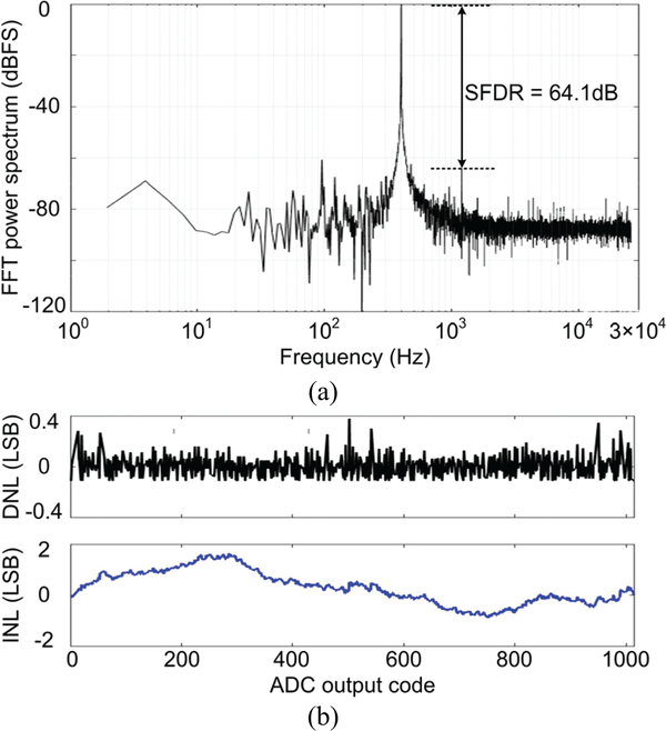
With a 1.8 VPP, 400 Hz sinusoidal waveform applied to the ADC input, we applied 2048-point fast-Fourier transformation (FFT) on the ADC output data bits. The produced FFT power spectrum indicates signal-to-noise ratio (SNR) of 54.2 dB and spurious-free dynamic range (SFDR) of 64.1 dB, representing effective number of bits (ENOB) of 8.7. To accurately measure differential nonlinearity (DNL) and integral nonlinearity (INL), a 0–1.8 V linear ramp with 100 bits per ADC output code was applied to the ADC, resulting in the DNL/INL resolution of 0.01 least significant bit (LSB). In Fig. 10b, the DNL and INL are within (+0.39, −0.12) LSB and (+1.50, −0.75) LSB, respectively.
Fig. 10.
(a) Measured 2048-point FFT power spectrum of the ADC output and (b) DNL and INL of the ADC.
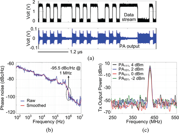
Fig. 11a shows the transient data transmission waveforms. The data bit stream OOK modulates the 434 MHz PA carrier. The PA with its output matched to the 50 Ω. impedance of the antenna transfers the data bits at a rate of 6.78 Mbps. Fig. 11b shows the measured PLL phase noise, which is −95.5 dBc/Hz at 1 MHz offset from 434MHz carrier. The spurs below 1 MHz are caused by interference from low-frequency reference clocks in the SoC. The induced interference on the 434 MHz carrier frequency is small, which does not corrupt functionality. Fig. 11c shows the measured PA output power under four different settings. The maximum output power of the PA is 4 dBm.
Fig. 11.
Measurement results of (a) data stream at the PA output, (b) PLL phase noise, and (c) Tx output power as a function of its 3 control bits.
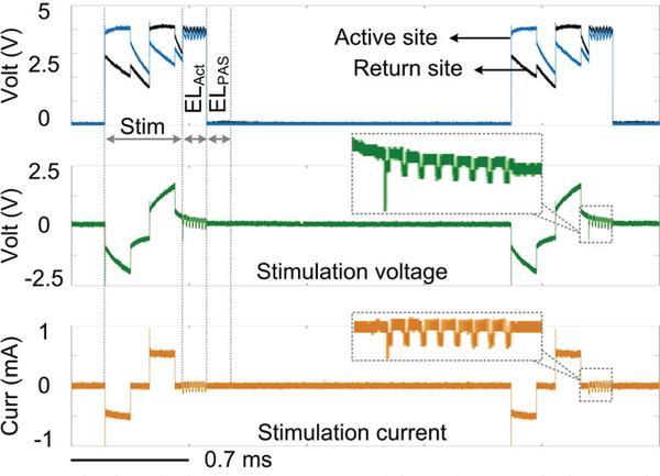
Fig. 12 presents the measured electrical stimulation waveforms while delivering current pulses with ±550 μA and 150 μs in amplitude and width, respectively. Pulses are delivered to the tissue model at 400Hz with 120 μs interphase delay. After stimulation, the voltage difference between two stimulating sites exceeds the upper bound of the ±50 mV safe window. The active CB circuit injects a series of 60 μA cathodic current pulses with 20 μs pulse width within 150 μs. It can be seen that the active CB circuit successfully returns the site voltage difference back within the safe window.
Fig. 12.
Measured stimulation waveforms with active CB being activation.
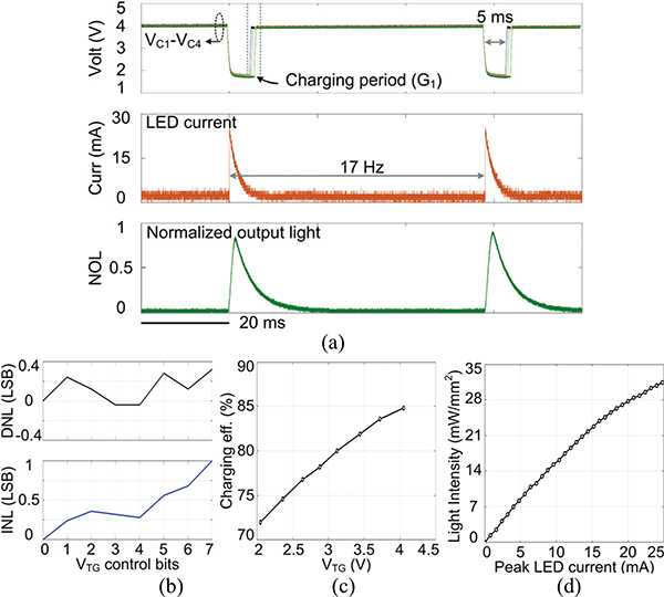
Fig. 13a presents the SCS operation to conduct optical stimulation with 5 ms pulse width at a rate of 17 Hz. The four capacitors in each group are charged to 4 V, and all four are selected to dump their charge into a selected μLED, creating an exponentially decaying current, which peak is limited to 24.8 mA. The emitted light from the μLED during stimulation pulse was collected by a photodetector (Newport 883-SL) connected to an optical power meter (Newport 1835-C). The normalized output light (NOL) expectedly follows the stimulation current variation with a slight delay. After each stimulation, all four capacitors are recharged back to 4 V. The target charging voltage, VTG, is adjustable from 2 V to 4 V by a 3-bit DAC, which DNL and INL are 0.32/−0.04 LSB and 1/0 LSB, respectively (Fig. 13b). The charging efficiency of this circuit changes from 72% to 84.8% depending on the target voltage, as shown in Fig. 13c. The charging efficiency is defined as the stored DC energy in the capacitor banks over the total input energy of the capacitor charging block during the charging period. Fig. 13d shows the light intensity under different current limits, which matches the μLED specifications [44]. We used μLED (TR2227TM, Cree) with a size of 220×270×50 μm3. The light intensity is calculated as the amount of light collected during a pulse divided by the surface area of the μLED, 220×270 μm2. Ignoring the losses, the peak value of the light intensity under 24.8 mA is 31.5 mW/mm2, which is well above the 1 mW/mm2 threshold of effective neuromodulation [33].
Fig. 13.
Measurement results of (a) charging a capacitor bank up to 4 V and discharging in a selected μLED for optical stimulation, (b) DNL and INL of the 3-bit DAC, (c) charging efficiency at different VTG, and (d) light intensity of the selected μLED as a function of the μLED current.
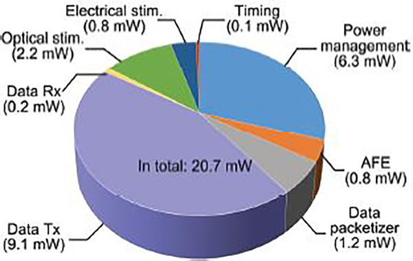
The average SoC power consumption is 20.7 mW when all three functions, neural recording, optical stimulation, and electrical stimulation, are enabled, and the two stimuli amplitudes are maxed out. The pie chart in Fig. 14 shows that the data Tx has the highest power consumption followed by the power management block. Table I summarizes the measured specifications of the trimodal SoC prototype.
Fig. 14.
Power consumption of the main blocks in the trimodal SoC
Table I:
Trimodal SoC Measured Specifications
| Optical Stimulation | Electrical Stimulation | ||
| VTG | 2–4 V, 3 bits | Charge balance | Active+Passive |
| Freq. | 2–50 Hz, 4 bits | Freq. | 8–400 Hz, 4 bits |
| Pulse width | 1.25–20 ms, 4 bits | Pulse width | 40–640 μs, 4 bits |
| Current | 0.8–24.8 mA, 5 bits | Current | ±(25–775) μA, 5 bits |
| Light intensity | 0–31.5 mW/mm2, 5 bits | Interphase delay | 40–640 μs, 4 bits |
| ADC | Data Tx | ||
| Sampling rate | 50 kS/s | Data carrier | RF 434 MHz, OOK |
| FoM | 78.6 fJ | Packet loss rate | <0.13% |
| DNL | (−0.12–0.39) LSB | Tx-Rx distance | Up to 150 cm |
| INL | (−0.75–1.5) LSB | Date rate | 6.78 Mbps |
| SNR | 54.2 dB | Output power | −3–4 dBm, 3 bits |
| SFDR | 64.1 dB | Data Rx | |
| ENOB |
8.7 |
Data carrier | Inductive link, 13.56 MHz, OOK |
|
Neural Recording | |||
| LNA gain | 40 dB | Data rate |
50 kbps |
| VGA gain | 15–30 dB, 3 bits |
SoC |
|
| Low cut-off | 1–100 Hz, 3 bits | Chip area | 3×5 mm2 |
| High cut-off | 10 kHz | Average power consumption | 20.7 mW |
| Input-referred noise | 3.46 μVrms with in 1 Hz-50 kHz | ||
| Supply volt. | 1.8/3.3/4V | ||
| NEF | 2.95 | Voltage doubler eff. | 82% |
| Recovery time | <0.4 ms | ||
V. In Vivo Experiment
A. In Vivo Experiment Design
To verify the functionality of the trimodal SoC, we conducted in vivo experiments on two male adult Sprague Dawley rats (350–400 g) by following our established protocols approved by the Institutional Animal Care and Use Committee (1ACUC) at Michigan State University. We injected adeno-associated virus (AAV) that carries optogenetics opsin (AAV-hSyn-hChR2 (H134R)-mCherry; UNC Vector Core) into each subject’s bilateral visual cortex (V1), using the stereotaxic surgery protocol in [20]. Then, we housed the subjects separately in the animal facility for postoperative recovery. For optogenetic neuromodulation, we waited 4 weeks following the virus injection to ensure that cortical neurons have expressed light excitability in channelrhodopsin-2 (ChR2).
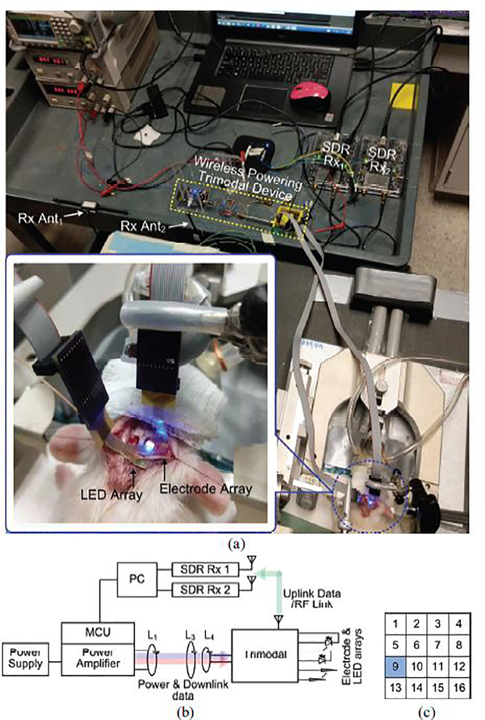
Although the in vivo setup in Fig. 15a shows the optical stimulation experiment, the same setup was used for performing electrical stimulation. Each subject received unilateral stimulation on the right V1 lobe, while the left V1 lobe of the same animal acted as control. A flexible 4×4 electrode array with channel arrangement shown in Fig. 15c was attached to the right V1 lobe. In Fig. 15b, a PA wirelessly delivered power to a trimodal evaluation board through a resonance-based multi-coil inductive link formed by a Tx coil, L1, and two Rx coils, L3 and L4. The current trimodal evaluation board with dimensions of 7 cm (length) × 5 cm (width) × 3 cm (height) and weight of l7 g was designed for verifying the functionality of the trimodal SoC in experiments with anesthetized animals. A microcontroller unit (MCU) OOK modulated the power carrier of the inductive link to send user-defined stimulation and recording parameters to the SoC. The SoC generated stimulation pulses, acting on the tissue where the Ch-9 electrode was located. At the same time, the SoC recorded local field potentials (LFP) from the 4×4 electrode array. The digitalized LFP data was wirelessly sent to our data acquisition system, in which a pair of SDR Rxs with orthogonal antennas picked up the OOK modulated RF signal and recovered the LFP data.
Fig. 15.
(a) In vivo experimental setup of performing optical stimulation, (b) Block diagram of the experimental setup, (c) Arrangement of the recording electrodes in an array.
In optical stimulation, a flexible 4×4 μLED array was placed above the electrode array and aligned to locate the selected μLED (220×270×50 μm3, TR2227TM, Cree) above the Ch-9 electrode. The selected μLED was driven by pulses with 5 ms width, 8 mA current limit, and 2 Hz frequency, resulting in light intensity of 11.8 mW/mm2. In electrical stimulation, the SoC injected ±100 μA pulses into a tungsten electrode, which reached the tissue at the depth of 100 μm underneath the Ch-9 electrode. The current pulses had 150 μs width, 150 μs interphase delay, and 8 Hz pulse rate.
In each stimulation mode, we compared the LFPs recorded in 4 conditions: LFP-I and LFP-II are LFPs recorded from Ch-9 and Ch-4 using trimodal SoC, respectively; LFP-III is spontaneous LFPs recorded from Ch-9 using trimodal SoC when stimulation is completely off (baseline), and LFP-IV is LFPs recorded from Ch-9 using a commercial Intan system (RHD2132) without artifact rejection function.
B. Electrical Stimulation Results
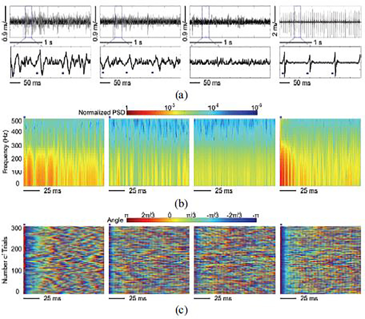
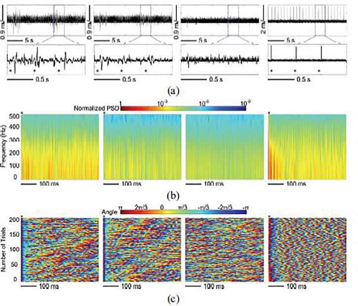
Fig. 16 compares the LFPs recorded in the abovementioned 4 conditions in terms of amplitude, power spectrum, and phase synchronization. Fig. 16a shows the sample recorded LFPs over a 2.5 s time span. The stimulation flags in the close-up view mark the stimulus pulses. Compared to the baseline, LFP-I and LFP-II were evoked by the electrical stimulation. Due to the reduced stimulation effect at Ch-4 location, LPF-II has lower amplitude than LFP-I. Without the artifact rejection function, large stimulus artifacts were observed in LFP-IV. In contrast, LFPs recorded using trimodal SoC were effectively protected from stimulus artifacts. We applied FFT on averaged LFPs over 100 electrical stimulations, resulting in time-frequency maps of the color-coded normalized power spectral density (PSD) [45]. As expected, LFP-I showed significant PSD upregulation. In contrast, the reduced stimulation effect in LFP-II only caused a slight increase in PSD as compared to the spontaneous LFPs. In LFP-IV, increase PSD at the onset of stimulus can be attributed to the artifacts. Moreover, we applied Hilbert transformation to extract the color-coded instantaneous phases of LFPs within 1–25 Hz frequency band over 300 stimulations [46]. The instantaneous phase of the LFPs over 300 stimulations were aligned to the concurrence of the stimulus and stacked, as shown in Fig. 16c. The spontaneous LFPs with random phases did not show phase synchrony. In contrast, long and reliable phase-locked synchronization was observed from the LFP-I across 300 stimulations. The instantaneous phase resulted from the LFP-II showed slight synchronization, as expected. The LFP-IV also had strong phase synchronization. However, it was induced by the strong and periodically repeated artifacts at the onset of each stimulation.
Fig. 16.
(a) Amplitude variation, (b) normalized PSD, and (c) instantaneous phases of LFP-I, LFP-II, LFP-III, and LFP-IV (from left to right) when the subject received electrical stimulation.
C. Optical Stimulation Results
Similarly, by comparing the amplitude, power spectrum, and instantaneous phase of the LFPs recorded in the above 4 conditions, we prove the efficacy of optical stimulation. Fig. 17 shows that LFP-I waveforms, which are closest to the stimulation source, have the largest amplitude variations, highest PDS elevation, and longest phase synchronization, compared to LFP-II and LFP-III. Moreover, although we still observed light-induced photoelectric artifacts along with LFPs in LFP-IV, the photoelectric artifacts were much smaller, compared to the electrical artifacts seen in Fig. 16. This result confirms a key advantage of optical stimulation over electrical stimulation, which is less disturbance in the simultaneous neuralrecording [15], [47].
Fig. 17.
(a) Amplitude variation, (b) normalized PSD, and (c) instantaneous phases of LFP-I, LFP-II, LFP-III, and LFP-IV (from left to right) when the subject received optical stimulation.
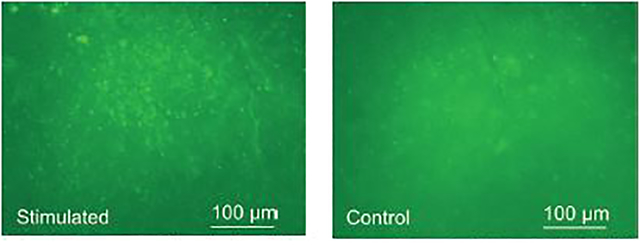
In addition to LFP comparison, we conducted immunostained tissue analysis. Fig. 18 shows the c-Fos fluorescent images of the post-processed 50 μm-thickness brain section, taken under 10× magnification. The green fluorescence spots indicated ChR2 transfected cells expressing c-Fos, a biomarker indicating the upregulation of neuronal activities induced by optical stimulation [48]. As opposed to the control side, increased c-Fos expression was observed in the stimulated V1 lobe.
Fig. 18.
C-Fos expression in the right (stimulated) vs. left (control) V1 lobes.
VI. In Vitro Experiment
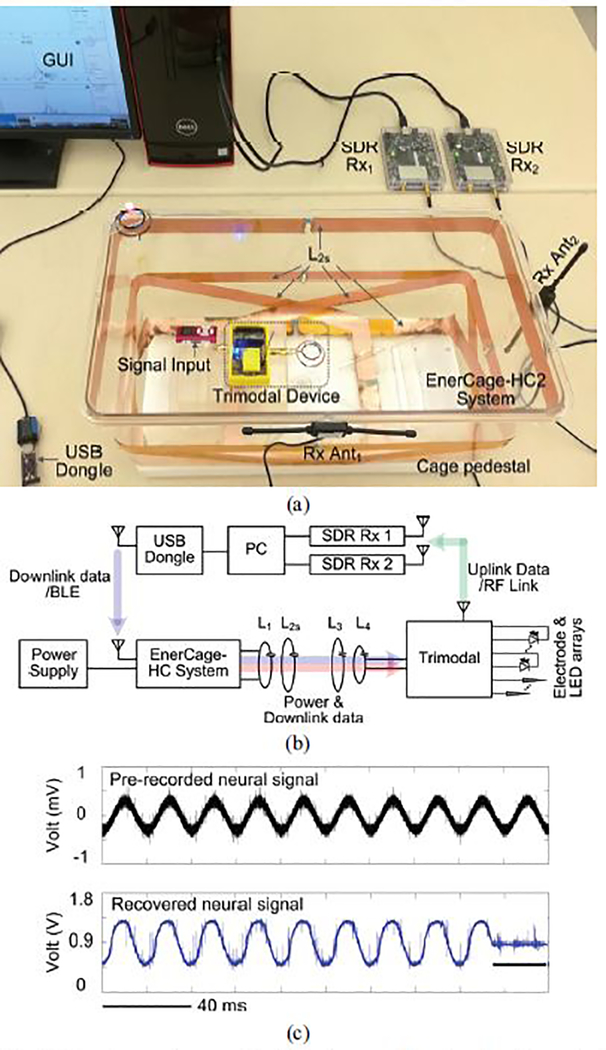
We have tested the feasibility of wirelessly powering the trimodal SoC in vitro using the EnerCage-HC system [31], [32]. In the experimental setup shown in Fig. 19, the EnerCage-HC system, built on a 13.56 MHz resonance-based 4-coil inductive link, delivered power and user-defined parameters to the trimodal SoC prototype board, which in turn drove a selected μLED while acquiring pre-recorded neural signals. Digitalized data was wirelessly transmitted via the 434 MHz RF link and picked up by the two SDR data Rxs outside of the homecage. To emulate a real recording, the pre-recorded neural signal contains spikes in hundreds of μVPP range added to a 50 Hz sinewave, which represents LFP in the background. Fig. 19c shows a short 2 s interval of the pre-recorded neural signal that was applied to the AFE (upper trace) and the recovered data by the SDR Rxs (lower trace). The stimulation flag indicated the optical stimulation pulse. In the trimodal SoC, the low cutoff frequency of the AFE was set at 1 Hz. It can be seen that both low-frequency LFP and spikes can be recovered. Besides, at the onset of optical stimulation, the recovered neural signal was pulled to the half of the supply voltage, which was performed by the artifact rejection circuit to protect the AFE from stimulus artifacts. These results can demonstrate the functionality of the trimodal SoC, wirelessly powered in the EnerCage-HC.
Fig. 19.
(a) Experimental setup of wirelessly powering the trimodal evaluation board in the EnerCage-HC system, (b) Block diagram of the experimental setup, (c) Recovered neural signal from the pre-recorded neural signal.
VII. Discussion
The main novelty of our work lies at the successful combination of circuit blocks for three individual modes of interfacing with the central nervous system (CNS) into a fully-integrated, wireless and battery-less, multi-functional and versatile neural interface SoC. As such, each circuit block was carefully designed for the purposes of power efficiency, design robustness, and reliable integration with each other as a whole. Besides, the specifications of the individual modalities remain competitive with state-of-the-art, such as the high current driving capability of the optical stimulation front-end, low noise level of the recording front-end, etc. The combination of benchtop, in votro, and in vivo results also validate the functionality and reliability of the novel trimodal SoC for its intended application.
Table I benchmarks the trimodal SoC prototype against recently reported neural interfaces, presenting its key advantages over the prior art. In terms of application, the trimodal SoC features wireless power and data transmission, which allows for long-term in vivo tests on freely behaving animal subjects, and a step closer to clinically viable devices in which wireless operation is necessary. Although using battery is a simpler option for power delivery, its limited lifetime will limit the experiment duration, not suitable for high power applications, such as optical stimulation.
In terms of system integration, this trimodal SoC features high-level integration by combining 16 neural recording channels, 8 biphasic electrical stimulation channels, 16 SCS-based optical stimulation channels, ADCs, wireless data Tx, wireless power and data Rxs, and digital blocks, all in a 5×3 mm2 silicon chip. The custom-designed SoCs presented in [14] and [19], on the other hand, still needs to work with commercial MCU for data transmission.
In terms of the versatility of neural interfacing modalities, we have demonstrated one of the most comprehensive multifunctional SoC, offering users flexibility to execute sophisticated hybrid neuromodulation paradigms. In [25], although all three functions are presented, the optical stimulation circuits are not fully integrated on chip, the recording/stimulation channel counts are limited to two/one, respectively, and the power source is still a battery with limited lifetime.
For the in vivo results, the LFP-based comparisons suggest that the electrical and optical stimulation applied using our trimodal SoC can effectively evoke neural activities, and the artifact rejection circuit can adequately prevent the LFPs from being submerged by the stimulus artifacts. The successful observation of neuronal oscillation, known as synchronized activities across the local population of neurons [49], proved the recording functionality of our SoC. The immunohistochemical analysis results further validated the efficacy of the optical stimulation.
The in vitro experiment is a major step towards developing a wireless implantable trimodal neural interface device, compatible with the EnerCage-HC system, to support in vivo experiments on small freely behaving animals over extended periods. Currently, we are developing a smaller version of the implantable trimodal device in a way that it can be attached to or implanted in small animal models without causing any discomfort or interference with their behavior.
As shown in Fig. 14, in addition to the data Tx block, the power management block also has high power consumption. To reduce it, we will improve the voltage doubler and LDOs. We have previously demonstrated an adaptive active voltage doubler/rectifier, which can automatically switch between active voltage doubler and active rectifier modes depending on which mode provides high power conversion efficiency (PCE) [50]. Besides this, we intend to design a boost converter, which features higher PCE than the current LDO.
VIII. Conclusion
We have presented a trimodal wireless implantable neural recording and optical/electrical stimulation SoC with all the necessary blocks to support wireless operation of these key neural interfacing functions. The AFE offers low-noise performance while the artifact rejection circuit can effectively prevent the AFE from being saturated by stimulus artifacts. The SCS method implemented in the SoC is capable of generating large instantaneous current pulses to drive selected μLEDs and generate light flashes that would surpass the optogenetic neuromodulation threshold. With both active and passive charge balancing, the SoC also ensures the safety of the biphasic electrical stimulation. The complete SoC functionality has been successfully verified both in vitro and in vivo on anesthetized rat model, while LFP signal and immunostained tissue analyses demonstrate functionality of the three neural interfacing modalities.
Table II:
Benchmarking of State-of-Art Multifunctional Neural Interface SoC
| Publication | 2017 [11] | 2019 [14] | 2018 [24] | 2018 [19] | 2019 [25] | This work |
| Technology | 0.13-μm | 0.18-μm+FPGA | 0.18-μm | 0.13-μm+MCU | 0.18-μm+COTS | 0.35-μm |
| No. interfacing modalities | 2 | 2 | 2 | 2 | 3 | 3 |
| No. recording channels | 64 | 128 | N/A | 10 | 2 | 16 |
| Input-referred noise / bandwidth | 1.13 μVrms / (0.1–500 Hz) | 1.6 μVrms / | N/A | 3.2 μVrms / (10 Hz-7 kHz) | 1.2 μVrms/ (25.4 Hz-25.6 kHz) | 3.46 μVrms / (1 Hz-50 kHz) |
| Channel gain / bandwidth | / (0.01–500 Hz) | / Up to 500 Hz | N/A | 46 dB / (0.5 Hz-7 kHz) | 27 dB / Up to 187.5 Hz | 55–70 dB / (1–100) Hz −10 kHz |
| Electrical stimulation channels | 64 | 128 | 4 | N/A | 1 | 8 |
| Electrical stimulation current | 10–1350 μA | 20 μA-5 mA | 22 μA-5 mA | N/A | 0–510 μA | 25–775 μA |
| Charge balancing | Yes | Yes | Yes | N/A | Yes | Yes |
| Optical stimulation channels | N/A | N/A | 1 | 4 | 1 | 16 |
| Optical stimulation current | N/A | N/A | 22 μA-5 mA | 0–35 mA | Up to 120 mA | 0.8–24.8 mA |
| Light intensity | N/A | N/A | Up to 23 mW/mm2 | N/A | Up to 50 mW/mm2 | Up to 31.5 mW/mm2 |
| Power transmission | Inductive link | Battery | Ultrasound | Battery | Battery | Inductive link |
| Downlink data | ASK / Inductive link | BLE | ASK / Ultrasound link | Nordic TRx | OOK TRx | OOK-PPM / Inductive link |
| Uplink data | UWB | BLE | N/A | Nordic TRx | OOK TRx | OOK / 434 MHz RF |
Acknowledgments
This work is supported in part by NSF awards ECCS-1407880 and ECCS-1408318, NIH award 1R21EB018561, NC State University, and NSF ASSIST Center (EEC-1160483).
Contributor Information
Yaoyao Jia, Department of Electrical and Computer Engineering, NC State University, Raleigh, NC, USA.
Ulkuhan Guler, Department of Electrical and Computer Engineering, Worcester Polytechnic Institute, Worcester, MA, USA.
Yen-Pang Lai, School of Electrical and Computer Engineering E, Georgia Tech, Atlants, GA, USA.
Yan Gong, Department of Electrical and Computer Engineering, Michigan State University, East Lansing, MI, USA.
Arthur Weber, Department of Physiology, Michigan State University, East Lansing, MI 48824, USA.
Wen Li, Department of Electrical and Computer Engineering, Michigan State University, East Lansing, MI, USA.
Maysam Ghovanloo, Bionic Sciences Inc., Atlanta, GA, USA.
Reference
- [1].Lebedev M, “Brain-machine interfaces: an overview,” Translational Neuroscience, vol. 5, no. l,pp. 99–110,2014. [Google Scholar]
- [2].Maharbiz MM, Muller R, Alon E, Rabaey JM, and Carmena JM, “Reliable next-generation cortical interfaces for chronic brain-machine interfaces and neuroscience,” Proceedings of the IEEE, vol. 105, no. 1, pp. 73–82, 2016. [Google Scholar]
- [3].Lebedev MA and Nicolelis MA, “Brain-machine interfaces: From basic science to neuroprostheses and neurorehabilitation,” Physiological Reviews, 2017. [DOI] [PubMed] [Google Scholar]
- [4].Santaniello S, Fiengo G, Glielmo L, and Grill WM, “Closed-loop control of deep brain stimulation: a simulation study,” IEEE Transactions on Neural Systems and Rehabilitation Engineering, vol. 19, no. 1, pp. 15–24, 2010. [DOI] [PubMed] [Google Scholar]
- [5].Nam CS, Nijholt A, and Lotte F, Brain-computer interfaces handbook: technological and theoretical advances. CRC Press, 2018. [Google Scholar]
- [6].Perlmutter JS and Mink JW, “Deep brain stimulation,” Annual Review of Neuroscience, vol. 29, pp. 229–257, 2006 [DOI] [PMC free article] [PubMed] [Google Scholar]
- [7].Sitaram R et al. , “Closed-loop brain training: the science of neurofeedback,” Nature Reviews Neuroscience, vol. 18, no. 2, pp. 86–100, 2017. [DOI] [PubMed] [Google Scholar]
- [8].Levi T, Bonifazi P, Massobrio P, and Chiappalone M, “Closed-loop systems for next-generation neuroprostheses,” Frontiers in Neuroscience, vol. 12, p. 26, 2018. [DOI] [PMC free article] [PubMed] [Google Scholar]
- [9].Liu X, Zhang M, Richardson AG, Lucas TH, and Van der Spiegel J, “Design of a closed-loop, bidirectional brain machine interface system with energy efficient neural feature extraction and PID control,” IEEE Transactions on Biomedical Circuits and Systems, vol. 11, no. 4, pp. 729–742, 2016. [DOI] [PubMed] [Google Scholar]
- [10].Greenwald E et al. , “A bidirectional neural interface IC with chopper stabilized BioADC array and charge balanced stimulator,” IEEE Transactions on Biomedical Circuits and Systems, vol. 10, no. 5, pp. 990–1002, 2016. [DOI] [PMC free article] [PubMed] [Google Scholar]
- [11].Kassiri H et al. , “Rail-to-rail-input dual-radio 64-channel closed-loop neurostimulator,” IEEE Journal of Solid-State Circuits, vol. 52, no. 11, pp. 2793–2810, 2017. [Google Scholar]
- [12].Cheng C-H et al. , “A fully integrated 16-channel closed-loop neural-prosthetic CMOS SoC with wireless power and bidirectional data telemetry for real-time efficient human epileptic seizure control,” IEEE Journal of Solid-State Circuits, vol. 53, no. 11, pp. 3314–3326, 2018. [Google Scholar]
- [13].Lee B et al. , “An inductively-powered wireless neural recording and stimulation system for freely-behaving animals,” IEEE Transactions on Biomedical Circuits and Systems, vol. 13, no. 2, pp. 413–424, 2019. [DOI] [PMC free article] [PubMed] [Google Scholar]
- [14].Zhou A et al. , “A wireless and artefact-free 128-channel neuromodulation device for closed-loop stimulation and recording in non-human primates,” Nature Biomedical Engineering, vol. 3, no. l,pp. 15–26,2019. [DOI] [PubMed] [Google Scholar]
- [15].Fan B and Li W, “Miniaturized optogenetic neural implants: a review,” Lab on a Chip, vol. 15, no. 19, pp. 3838–3855, 2015. [DOI] [PubMed] [Google Scholar]
- [16].Goncalves S, Ribeiro J, Silva A, Costa R, and Correia J, “Design and manufacturing challenges of optogenetic neural interfaces: a review,” Journal of Neural Engineering, vol. 14, no. 4, p. 041001, 2017. [DOI] [PubMed] [Google Scholar]
- [17].Montgomery KL et al. , “Wirelessly powered, iully internal optogenetics for brain, spinal and peripheral circuits in mice,” Nature Methods, vol. 12, no. 10, pp. 969–974, 2015. [DOI] [PMC free article] [PubMed] [Google Scholar]
- [18].Shin G et al. , “Flexible near-field wireless optoelectronics as subdermal implants for broad applications in optogenetics,” Neuron, vol. 93, no. 3, pp. 509–521. e3, 2017. [DOI] [PMC free article] [PubMed] [Google Scholar]
- [19].Gagnon-Turcotte G, Khiarak MN, Ethier C, De Koninck Y, and Gosselin B, “A 0.13-pm CMOS SoC for simultaneous multichannel optogenetics and neural recording,” IEEE Journal of Solid-State Circuits, vol. 53, no. 11, pp. 3087–3100, 2018. [Google Scholar]
- [20].Jia Y et al. , “Wireless opto-electro neural interface for experiments with small freely behaving animals,” Journal of Neural Engineering, vol. 15, no. 4, p. 046032, 2018. [DOI] [PMC free article] [PubMed] [Google Scholar]
- [21].Ramezani R et al. , “On-probe neural interface ASIC for combined electrical recording and optogenetic stimulation,” IEEE Transactions on Biomedical Circuits and Systems, vol. 12, no. 3, pp. 576–588, 2018. [DOI] [PubMed] [Google Scholar]
- [22].Jia Y et al. , “A mm-sized free-floating wirelessly powered implantable optical stimulation device,” IEEE Transactions on Biomedical Circuits and Systems, vol. 13, no. 4, pp. 608–618, 2019. [DOI] [PMC free article] [PubMed] [Google Scholar]
- [23].Chapman CA, Goshi N, and Seker E, “Multifunctional neural interfaces for closed - loop control of neural activity,” Advanced Functional Materials, vol. 28, no. 12, p. 1703523, 2018. [Google Scholar]
- [24].Charthad J et al. , “A mm-sized wireless implantable device for electrical stimulation of peripheral nerves,” IEEE Transactions on Biomedical Circuits and Systems, vol. 12, no. 2, pp. 257–270, 2018. [DOI] [PubMed] [Google Scholar]
- [25].Lee S-Y et al. , “A programmable wireless EEG monitoring SoC with open/closed-loop optogenetic and electrical stimulation for epilepsy control,” in 2019 IEEE International Solid-State Circuits Conference- (ISSCC), 2019: IEEE, pp. 372–374. [Google Scholar]
- [26].Jia Y et al. , “A trimodal wireless implantable neural interface system-on-chip,” in 2020 IEEE International Solid-State Circuits Conference-(ISSCC), 2020: IEEE, pp. 414–416. [DOI] [PMC free article] [PubMed] [Google Scholar]
- [27].Wang J et al. , “Integrated device for combined optical neuromodulation and electrical recording for chronic in vivo applications,” Journal of Neural Engineering, vol. 9, no. 1, p. 016001, 2011. [DOI] [PubMed] [Google Scholar]
- [28].Shulyzki R et al. , “320-channel active probe for high-resolution neuromonitoring and responsive neurostimulation,” IEEE Transactions on Biomedical Circuits and Systems, vol. 9, no. 1, pp. 34–49, 2014. [DOI] [PubMed] [Google Scholar]
- [29].Luo Z and Ker M-D, “A high-voltage-tolerant and power-efficient stimulator with adaptive power supply realized in low-voltage CMOS process for implantable biomedical applications,” IEEE Journal on Emerging and Selected Topics in Circuits and Systems, vol. 8, no. 2, pp. 178–186, 2018. [Google Scholar]
- [30].Mei H, Thackston KA, Bercich RA, Jefferys JG, and Irazoqui PP, “Cavity resonator wireless power transfer system for freely moving animal experiments,” IEEE Transactions on Biomedical Engineering, vol. 64, no. 4, pp. 775–785, 2016. [DOI] [PubMed] [Google Scholar]
- [31].Mirbozorgi SA, Jia Y, Canales D, and Ghovanloo M, “A wirelessly-powered homecage with segmented copper foils and closed-loop power control,” IEEE Transactions on Biomedical Circuits and Systems, vol. 10, no. 5, pp. 979–989, 2016. [DOI] [PMC free article] [PubMed] [Google Scholar]
- [32].Jia Y et al. , “Position and orientation insensitive wireless power transmission for EnerCage-Homecage system,” IEEE Transactions on Biomedical Engineering, vol. 64, no. 10, pp. 2439–2449, 2017. [DOI] [PMC free article] [PubMed] [Google Scholar]
- [33].Stark E, Koos T, and Buzsaki G, “Diode probes for spatiotemporal optical control of multiple neurons in freely moving animals,” Journal of Neurophysiology, vol. 108, no. 1, pp. 349–363, 2012. [DOI] [PMC free article] [PubMed] [Google Scholar]
- [34].Jia Y et al. , “A software-defined radio receiver for wireless recording from freely behaving animals,” IEEE Transactions on Biomedical Circuits and Systems, vol. 13, no. 6, pp. 1645–1654, 2019. [DOI] [PMC free article] [PubMed] [Google Scholar]
- [35].Lee H-M, Kwon KY, Li W, and Ghovanloo M, “A power-efficient switched-capacitor stimulating system for electrical/optical deep brain stimulation,” IEEE Journal of Solid-State Circuits, vol. 50, no. 1,pp. 360–374, 2014. [Google Scholar]
- [36].Merrill DR, Bikson M, and Jefferys JG, “Electrical stimulation of excitable tissue: design of efficacious and safe protocols,” Journal of Neuroscience Methods, vol. 141, no. 2, pp. 171–198, 2005. [DOI] [PubMed] [Google Scholar]
- [37].Lee H-M, Park H, and Ghovanloo M, “A power-efficient wireless system with adaptive supply control for deep brain stimulation,” IEEE Journal of Solid-State Circuits, vol. 48, no. 9, pp. 2203–2216, 2013. [DOI] [PMC free article] [PubMed] [Google Scholar]
- [38].Lee B and Ghovanloo M, “An adaptive averaging low noise front-end for central and peripheral nerve recording,” IEEE Transactions on Circuits and Systems II: Express Briefs, vol. 65, no. 7, pp. 839–843,2017. [DOI] [PMC free article] [PubMed] [Google Scholar]
- [39].Rezaee-Dehsorkh H, Ravanshad N, Lotfi R, Mafmezhad K, and Sodagar AM, “Analysis and design of tunable amplifiers for implantable neural recording applications,” IEEE Journal on Emerging and Selected Topics in Circuits and Systems, vol. 1, no. 4, pp. 546–556, 2011. [Google Scholar]
- [40].Tong X and Zhang Y, “98.8% switching energy reduction in SAR ADC for bioelectronics application,” Electronics Letters, vol. 51, no. 14, pp. 1052–1054, 2015. [Google Scholar]
- [41].Liu C-C, Chang S-J, Huang G-Y, and Lin Y-Z, “A 10-bit 50-MS/s SAR ADC with a monotonic capacitor switching procedure,” IEEE Journal of Solid-State Circuits, vol. 45, no. 4, pp. 731–740, 2010. [Google Scholar]
- [42].Lee B et al. , “An implantable peripheral nerve recording and stimulation system for experiments on freely moving animal subjects,” Scientific Reports, vol. 8, no. 1, pp. 1–12, 2018. [DOI] [PMC free article] [PubMed] [Google Scholar]
- [43].Jia Y and Ghovanloo M, “Towards a mm-Sized Free-Floating Wireless Implantable Opto-Electro Stimulation Device,” in 2019 IEEE Biomedical Circuits and Systems Conference (BioCAS), 2019: IEEE,pp. 1–4 [Google Scholar]
- [44].“Cree TR2227 LEDs Datasheet,” Cree; Durham, NC: TR™ LEDs, September 2019. [Online] Available: https://www.cree.com/led-chips/media/documents/CPR3EF.pdf [Google Scholar]
- [45].Schalk G and Leuthardt EC, “Brain-computer interfaces using electrocorticographic signals,” IEEE Reviews in Biomedical Engineering, vol. 4, pp. 140–154, 2011. [DOI] [PubMed] [Google Scholar]
- [46].Le Van Quyen M et al. , “Comparison of Hilbert transform and wavelet methods for the analysis of neuronal synchrony,” Journal of Neuroscience Methods, vol. III, no. 2, pp. 83–98, 2001. [DOI] [PubMed] [Google Scholar]
- [47].Kwon KY, Sirowatka B, Weber A, and Li W, “Opto-μECoG array: A hybrid neural interface with transparent μECoG electrode array and integrated LEDs for optogenetics,” IEEE Transactions on Biomedical Circuits and Systems, vol. 7, no. 5, pp. 593–600, 2013. [DOI] [PubMed] [Google Scholar]
- [48].Kawashima T, Okuno H, and Bito H, “A new era for functional labeling of neurons: activity-dependent promoters have come of age,” Frontiers in Neural Circuits, vol. 8, p. 37, 2014. [DOI] [PMC free article] [PubMed] [Google Scholar]
- [49].Kwon KY, Aviyente S, and Li W, “Investigation of phase-locked neuronal oscillation with optical stimulation based on a time-frequency approach,” in 2013 6th International IEEE/EMBS Conference on Neural Engineering (NER), 2013: IEEE, pp. 423–426. [Google Scholar]
- [50].Lee H and Ghovanloo M, “An adaptive reconfigurable active voltage doubler/rectifier for extended-range inductive power transmission,” IEEE Transactions on Circuits and Systems II: Express Briefs, vol. 59, no. 8, pp. 481–485, August 2012. [DOI] [PMC free article] [PubMed] [Google Scholar]


