

Abstract

Metastable single crystals of nonstoichiometric Pb1–xTe are obtained by rapid cooling from the melt. The composition and crystallographic morphology are studied using X-ray diffraction, scanning electron microscopy, energy-dispersive X-ray spectroscopy, and electron backscatter diffraction. Most single crystals have cubic, pyramidal, or hemispherical shapes with sizes ranging from 50 to 400 μm. All crystals adopt the same face-centered cubic rock salt structure, and the crystal growth direction is ⟨100⟩. The bulk part of the rapidly cooled material solidifies in the form of a Te-rich polycrystalline material in which grains are separated by the PbTe–Te eutectic phase. The stabilization of nonstoichiometric Pb1–xTe provides further scope for the optimization of lead telluride-based thermoelectric materials.
Keywords: lead telluride, thermoelectrics, nanostructures, single crystals, electron backscatter diffraction
1. Introduction
Lead telluride (PbTe) has attracted much attention since the 1950s due to its unique physicochemical properties. After more than 60 years, PbTe still has value for exploration and research, giving inspiration not only with respect to application and performance but also regarding its structure and morphology. As part of the family of IV–VI narrow-band-gap semiconductors, it has found use mainly as a thermoelectric material for power generation in the 500–800 K range1−3 and also in infrared detectors and tunable diode lasers.4 Concerning thermoelectric applications, modifications to PbTe are still leading to improvements in its performance. For example, Biswas et al. incorporated SrTe nanoparticles in p-type Na-doped PbTe to achieve a figure of merit (ZT) of 2.2,5 and more recently, Wu et al. achieved a ZT of 2.5 by alloying Na-doped PbTe with EuTe and CdTe.6 Efforts have also been made to enhance the performance of n-type PbTe, for example, by Sb-doping.7 You et al. recently showed that the so-called dynamic doping, involving the introduction of Cu atoms on the interstitial sites of PbTe, can also enhance ZT.8 Concurrently, detailed attempts to control the chemical synthesis of doped PbTe have been reported,9 and progress has been made toward its incorporation in working modules.10 An alternative approach involves complex nanostructuring; for example, Xiang et al. created composites of pristine PbTe nanoparticles combined with C- and Ag-coated PbTe nanoparticles in order to control both the electron and phonon transport.11 There is also a great deal of interest in the growth of anisotropic PbTe nanostructures. The most widely used approaches are wet chemical methods,12 electrodeposition methods,13 sonochemical approaches,14 and thin-film growth.15 Various types of nanostructures have been reported, including nanorods,16 nanotubes,17 nanocubes,18 nanowires,19−21 quantum dots,22 and nanoboxes.23
Thus far, it has generally been assumed that PbTe is stoichiometric. According to the Pb–Te equilibrium binary phase diagram,24 when the atomic ratio of Te in the liquid phase is more than 50%, stoichiometric PbTe will be continuously precipitated when the temperature is decreased slowly below the liquidus line. When the temperature is lowered further below the eutectic temperature of 410 °C, a eutectic of two phases (PbTe and Te) solidifies from the rest of the liquid phase. However, a study by Glazov and Poyarkov25 addressed the possibility of stabilizing nonstoichiometric Pb1–xTe by rapid quenching from the melt. It was argued that at Te concentrations of >50 at. %, fast quenching can give rise to diffusionless solidification, which allows nonstoichiometric compositions to be obtained at room temperature. Although adjusting the stoichiometry might provide a new route toward tuning the properties of PbTe, this possibility has to the best of our knowledge not been investigated further.
In this work, we show that nonstoichiometric Pb1–xTe single crystals of several different morphologies as well as polycrystalline materials can be obtained by rapid cooling of the Pb–Te melt in vacuum. In order to understand the relationship between the morphology and composition of these products, we study them separately using single-crystal X-ray diffraction (XRD), scanning electron microscopy (SEM) equipped with energy-dispersive X-ray spectroscopy (EDS), and electron backscatter diffraction (EBSD). According to our knowledge, EBSD is used here for the first time to align the macroscopic crystal shape with its crystallographic orientation.
2. Experimental Section
2.1. Crystal Synthesis
The Pb1–xTe samples were prepared by fast quenching from the melt. Elemental Pb powder (∼5 μm, Alfa Aesar) and Te shot (∼5 mm, Alfa Aesar) of 99.99% purity (total mass ∼5 g) with the molar ratio 1:1 were mixed for 15 min using an agate mortar and pestle, flame-sealed in a quartz tube that was evacuated to 10–1 to 10–2 mbar, and then heated over 3 h to 1000 °C. At this temperature, the mixture is in the liquid phase,24 where it was held for 3 h before quenching by removing the quartz tube from the furnace and immediately dropping it into 20 L of room-temperature water. A large number of single crystals (100–300 μm in size) were obtained together with a larger volume of polycrystalline bulk material. An optical microscope was used to collect the single crystals, which were both attached to the bulk material and to the inner wall of the quartz tube.
2.2. Characterization Methods
The structure of the crystals was characterized by single-crystal XRD using a Bruker D8 Venture diffractometer operating with Mo Kα radiation and equipped with a Photon100 area detector and a Triumph monochromator. Each single crystal was fixed on a 0.3 mm diameter nylon loop using cryo-oil and maintained at a temperature of 100 K during the measurement by a flow of dry nitrogen. Bruker APEX III software was used for data processing and SHELX97 software was used to refine the crystal structure.26 Powder XRD patterns were collected on the bulk material using a Bruker D8 ADVANCE diffractometer with Cu Kα radiation. The diffraction patterns were fitted using GSAS software.27
The microstructure of both the single crystals and bulk material was studied using SEM, EDS, and EBSD using a FEI Nova NanoSEM 650 equipped with an EDAX EDS/EBSD system with an Octane SDD EDS detector and Hikari Plus EBSD camera. Team v.4.5 and OIM Analysis v.8.1 software were used to perform semiquantitative EDS and EBSD data analysis, respectively. The cubic structure of PbTe with a lattice parameter of 0.64 nm and the set of main reflector planes (200), (220), (222), (420), (422), and (442) were successfully used to index all the obtained Kikuchi patterns and determine the single-crystal orientation. The common electron beam acceleration voltage for EDS and EBSD observations was selected as 25 kV, which allows reliable semiquantitative EDS analysis on the basis of the Lα peaks of both elements and also provides a reasonably strong EBSD pattern for crystal orientation determination. Detailed EDS measurements were performed at a lower acceleration voltage of 10–15 keV which corresponds to an EDS probing depth of 0.4–0.7 μm.
The thermal diffusivity (α) of the bulk material was measured by the laser flash method in a Linseis LFA1000 apparatus. A sample that was visually free of cracks and holes was cut from the bulk and polished to a slice of 4.0 × 3.9 × 0.9 mm. Data were collected on warming from room temperature to 400 °C with 25 °C steps. The thermal conductivity (κ) was determined using the relation κ = αρCp, where ρ is the sample density and the specific heat capacity (Cp) was calculated using the Dulong–Petit approximation.
3. Results and Discussion
Four kinds of samples were identified under the optical microscope and deemed worthy of the in-depth study: cubic-shaped single crystals, prismatic-shaped single crystals, hemispherical-shaped single crystals, and bulk polycrystalline material. The structure and morphology of each sample type were studied separately, and their similarities and differences are discussed below.
3.1. Crystal Structure Analysis
The morphologies of the single crystals fall into two broad categories: one type has well-defined facets and edges and includes cubes, triangular pyramids, and asymmetrical prisms; the other type has the form of a hemispherical droplet with one approximately flat face. Figure 1a–c shows the (hk0) reciprocal lattice planes reconstructed from raw single-crystal XRD data for three representative single crystals with different morphologies at 100 K. The crystals show slightly different lattice parameters but are all close to the value of 6.438 Å reported for PbTe at 120 K.28Figure 1d shows the single-crystal XRD data at 300 K for the triangular pyramid. The data are consistent with space group Fm3̅m for all three crystals. In Figure 1b,c, the spots are rather broad, especially at high angles, suggesting the presence of multiple mosaic blocks. In Figure 1c, two faint polycrystalline rings are apparent near the center of the reciprocal lattice plot, indexed as 200 and 220. Nevertheless, the well-defined spots indicate that the major volume fraction of the hemispherical sample is a cubic rock salt single crystal.
Figure 1.

(hk0) reciprocal lattice planes reconstructed from raw single-crystal XRD data at 100 K for the (a) triangular pyramid, (b) asymmetrical prism, and (c) hemispherical droplet. (d) Single-crystal XRD data at 300 K for the triangular pyramid. (e) Fitted powder XRD pattern of the polycrystalline bulk material collected at room temperature: Rp = 6.64%, Rwp = 9.50%, and Rexp = 1.13%.
The powder XRD pattern collected on the bulk material in Figure 1e reveals the presence of Te in addition to the main PbTe phase. The lattice parameter of the main PbTe phase is 6.4663(3) Å, which is slightly above the range of 6.455–6.465 Å reported in various room-temperature studies and listed in the Inorganic Crystal Structure Database. The lattice parameter of the triangular pyramid determined at 300 K by single-crystal XRD is 6.4664(4) Å, which agrees well with that of the bulk sample.
3.2. Morphological Analysis
3.2.1. Pyramids and Prisms
The sizes of the single crystals with a pyramidal and prismatic morphology are between 50 and 400 μm. As shown in Figure 2, in each single crystal at least one right angle between crystal faces can be observed, and in the prisms there is another angle between 0 and 45°. In these SEM-BSE (backscattered electron) images, a brighter contrast corresponds to a greater concentration of heavier (Pb) atoms. In Figure 2a,c, the surfaces of the single crystals exhibit some spots and ring-like features, while in Figure 2b,d, the surfaces of the single crystals are compositionally homogeneous (the dark patches on the sample surface in Figure 2b are shown by EDS to be residual silicone-based oil that was used to transfer the crystals; EDS spectra from these areas are almost identical to those collected from neighboring (uncontaminated) regions except for the presence of small carbon, silicon, and oxygen peaks). Pits are visible in many of the surfaces and are likely formed by the Berg effect,29,30 where the concentration of liquid or vapor is greater near the corners or edges of a growing crystal than at the centers of the faces.
Figure 2.

(a–d) SEM-BSE images of some pyramidal- and prismatic-shaped PbTe single crystals. (e,f) Secondary electron (SE) image (left, 71° tilt), EBSD pattern (top right), and determined top-view crystal orientation (bottom right) for the crystals shown in (a,c), respectively.
In order to identify the crystallographic planes associated with individual faces of the single crystals, we used EBSD to determine the orientation of each crystal lying on the flat aluminum (Al) substrate. Figure 2e,f demonstrates such an observation for two single crystals when the substrate normal is tilted 71° to the electron beam direction. Kikuchi patterns (top right) were collected from a few surface points to prove that they are single crystals, and their correct indexing results in three Euler angles determining the crystal orientation in the sample coordinate system.
Axonometric projections of the cubic crystal orientations (top view) are shown in the lower right parts of the two figures. The agreement between the ⟨001⟩ crystal axes in the axonometric projections and the edges of the crystals in the SEM images proves that the crystal faces are {001} planes, which was the case for every pyramidal- and prismatic-shaped crystal investigated. Crystals of cubic morphology usually grow in the ⟨100⟩ direction, which requires lower energy.31 Furthermore, planar growth in the ⟨100⟩ direction is also observed in the form of steps on the {100} facets, which are particularly obvious in pits on these facets as apparent in Figure 2a,d.32 The {100} planes also seem to be cleavage planes (see Figure S1).
The surfaces of pyramidal and prismatic single crystals that exhibit both light and dark contrast in the SEM-BSE images were further investigated using EDS. The results for the two representative samples are summarized in Figure 3. Figure 3a shows the BSE image of one (001) facet of the pyramid from Figure 2a. EDS elemental maps of Pb and Te (collected from the rectangular area marked on the BSE image) clearly indicate the presence of two types of domains, in agreement with the BSE image; the brighter areas represent lead-rich areas, and the darker spots correspond to lead-deficient areas. The atomic Pb/Te ratio calculated from the spectrum collected from the whole mapped area is 33:67. The average atomic ratios of Pb to Te determined from many points in the main phase (bright) region and lead-deficient (dark) regions are 41:59 and 17:83, respectively. Thus, the entire area is Te-rich with respect to the nominal 1:1 stoichiometry, and the dark spots and ring-like features on the (001) surfaces of the single crystals are even more Te-rich. EDS analysis performed on the surface of the single crystal in Figure 2b with a uniform contrast yielded a Pb to Te atomic ratio of 43:57 (Figure 3b), which is similar to the composition of the main phase in Figure 3a. The areas of dark contrast in Figure 3b are due to surface contamination by the oil used for crystal manipulation. The otherwise uniform contrast implies that all faces show a homogeneous composition.
Figure 3.

SEM-BSE images of (a) one surface of the pyramidal single crystal shown in Figure 2a and (b) two faces of the prismatic crystal shown in Figure 2b. The rectangles on the SEM images indicate areas over which EDS spectra were measured; the corresponding compositions (at. %) of Te and Pb are shown in the tables.
The above cases are representative of more than a dozen faceted single-crystal samples that were studied; that is, sometimes the sample surface is homogeneous and sometimes Te-rich spots and rings appear. We propose that these crystals grow directly from the vapor phase due to the rapid cooling rate, as shown schematically in Figure 4. Nucleation (step 1) occurs on a relatively flat surface (the inner wall of the quartz tube or the surface of the material that has already solidified) and growth then occurs along the {100} planes (step 2). Step 3 shows two different situations during the final growth phase in which the vapor has almost all condensed. Due to the lower melting point of Pb compared to that of Te, we suspect that some of the Pb vapor present during growth will either react with residual water vapor in the quartz tube or condense on the inner wall of the tube, both of which lower the partial vapor pressure of Pb and cause Te enrichment in the synthetic environment. This will in turn produce the observed 2–5 μm Te-rich spots as well as Te-rich dendrites on the (100) surface. Other areas will not be exposed to excess Te vapor at the crystal surface, and the resulting (100) plane will be homogeneous in composition.
Figure 4.

Schematic diagram of single-crystal growth on the flat quartz tube wall. The SEM images show Te-rich spots and dendrites on a crystal surface.
The Pb-deficiency of these single crystals (as compared to the equimolar starting composition) can also be explained by the Te-rich growth environment. There are only a small number of reports suggesting that PbTe can be stabilized in a nonstoichiometric form, which is unexpected based on the Pb–Te binary phase diagram.24 In the work of Ovsyannikov et al.,33 the crystal structures of polycrystalline samples with compositions Pb0.45Te0.55 and Pb0.55Te0.45 were studied at high pressure, but no chemical analysis was presented nor were details of how these phases formed. Bauer Pereira et al.34 also performed water quenching of PbTe from the melt and obtained a sample of composition Pb0.94Te with a lattice parameter of 6.461(3) Å at room temperature, slightly smaller than our sample, but did not study the growth process or morphological characteristics. To the best of our knowledge, the most detailed study of nonstoichiometric Pb1–xTe remains that of Glazov and Poyarkov,25 which suggests that the composition can be tuned over a relatively wide range on the Te-rich side of the phase diagram while retaining the cubic rock salt structure. It was reported that quenching must be performed from 1000 °C to obtain the nonstoichiometric cubic phase; quenching from 800 °C gave a mixture of PbTe and Te (the latter phase possibly containing a little Pb). The room-temperature lattice parameter of the cubic phase was reported as 6.465 Å at 74 at. % Te (similar to our value for the bulk material) and rapidly increased at higher Te concentrations. It was suggested that the faster the cooling rate, the wider the composition range that can be stabilized at room temperature.
3.2.2. Droplet-Shaped Crystals
An example of a hemispherical crystal and its microstructural characterization is shown in Figure 5. Figure 5a shows a full view of a hemispherical crystal. A complex microstructure is formed on its flat surface, as seen in Figure 5b,b1. Primary dendrites with light contrast, partially decomposed into two phases (see detail in Figure 5b1), are surrounded by a matrix that itself consists of very fine lamellae with light contrast dispersed in a dark (Te-rich) surrounding. The overall sample composition (Pb/Te atomic ratio) calculated from the elemental map in Figure 5d is 18:82; in the primary dendrite region (the large bright areas in Figure 5b,b1), the ratio is 40:60, and in the Te-rich region, it is 7:93 (very close to the eutectic composition of 89.1 at. % Te21). A BSE image from the spherical surface (Figure 5c) shows a different volume ratio between the primary dendrites and the interdendritic phase than the flat surface in Figure 5b due to two main reasons: (i) the dendrites do not look to be decomposed and (ii) the interdendritic phase is sunk down below the surface. Accurate EDS measurements cannot be obtained from a surface that is not flat; thus, the composition of the spherical surface could not be quantitatively determined.
Figure 5.

SEM-BSE images of the (a) hemispherical crystal; (b) and (b1) details from the flat surface; (c) details from the spherical surface; and (d,e) corresponding EDS elemental maps from images (b,c), respectively.
These microstructural observations suggest a scenario involving the rapid solidification of liquid droplets sitting on a cooled solid surface, probably the wall of the quartz tube. According to the equilibrium binary phase diagram,24 when a melt with a Pb/Te composition of 18:82 is cooled, it will first form a gradually growing primary PbTe phase (50:50 at. %) in a liquid with a gradually increasing amount of Te. At the eutectic temperature of ∼410 °C, this liquid phase reaches the eutectic composition and solidifies as the eutectic phase. However, the cooling rate of our samples was relatively high; therefore, the formation of metastable phases can be expected. The primary phase will not be PbTe but a metastable phase with an excess amount of Te because diffusion is not able to remove all the excess Te atoms trapped in the solidified primary phase. Due to fast cooling and limited diffusion, this primary phase forms a dendritic structure with the liquid phase remaining between the dendrites. This liquid will solidify as a fine eutectic between the primary dendrites. The primary dendrites supersaturated by Te will then partially disintegrate, forming another fine eutectic in the microstructure. All the above-mentioned microstructural features are directly visible in Figure 5b,b1.
Similar to the prismatic crystals, the atomic ratio of Pb to Te in the primary dendrites of both the hemispherical flat surface and the curved surface is approximately 2:3. This fact suggests that similar cooling rates were involved during the vapor-phase growth of the prismatic single crystals and during solidification of the melt droplets, allowing a similar degree of supersaturation of Te atoms into the PbTe single crystal.
Figure 6 shows an EBSD microstructural characterization of a large area of the flat surface of the hemispherical sample. Figure 6a is an image quality map clearly showing the size and distribution of the primary phase dendrites and the Te-rich pseudoeutectic matrix giving patterns of similar quality. The corresponding inverse pole figure map in Figure 6b was obtained by indexing the EBSD patterns collected while scanning the whole area assuming the presence of the same cubic phase. The grain orientation of the entire crystal is essentially the same with one ⟨001⟩ direction almost parallel to the flat surface normal. The local variation of the crystal orientation is visualized in Figure 6c where the average grain orientation angle deviating from the crystal orientation at the scan center is shown. In the entire area, all pixels show a deviation from one direction of less than 10°. This implies that (i) the whole crystal grows as a single dendrite, and individual dendrite arms may gather a misorientation with increasing distance from the origin of nucleation and (ii) subsequent solidification of the eutectic phase also forms a cubic crystalline structure growing epitaxially on the adjacent dendrite. Although three different solid phases (primary Pb1–xTe and Te-rich eutectic) are present in the hemispheric droplet, the whole droplet can be considered as a single cubic crystal with mutual misorientations of blocks smaller than 10°.
Figure 6.

EBSD mapping from a 40 × 50 μm2 area on the flat surface of the hemispherical sample shown in Figure 5a. (a) Image quality map quantifying the contrast of EBSD patterns collected from individual pixels; (b) [001] inverse pole figure map taken from the same area showing nearly the same crystal direction throughout the area probed: [001] is almost parallel to the sample surface normal with the (001) pole figure inset showing an almost uniform crystal orientation; (c) grain reference orientation deviation angle map demonstrating how the local misorientation between individual dendrites develops. White areas on the maps indicate pixels with bad quality and therefore unindexed Kikuchi patterns.
The curved surface of the droplet is not ideally spherical but shows some traces (marked by arrows) of preferential growth direction as the SE image in Figure 7a demonstrates. The fact that these traces can be associated with the traces of crystallographic planes (as shown in Figure 7e for the {111} planes) is additional confirmation that the whole droplet comprises one single cubic crystal as shown by single-crystal XRD. The growth of the nucleus in the droplet also follows the growth direction of the cubic crystal.
Figure 7.

(a) SEM top view of the hemispherical crystal with clear “meridian” lines on the spherical surface. (b) EBSD pattern, (c) properly indexed EBSD pattern, and (d) (100) pole figure. (e) Traces of {111} planes agreeing with main meridian lines.
3.2.3. Polycrystalline Bulk
Figure 8 summarizes the microstructural characterization of a polished cross section of the polycrystalline bulk material. Figure 8a is a forward-scattered electron (FSE) image from a large area of 333 × 784 μm2. A typical polycrystalline structure containing primary grains of size 100–300 μm in diameter with the eutectic phase between them is clearly present. EDS analysis performed on the large area shows that the average composition of the bulk sample has a Pb/Te ratio of 39:61 at. %. Figure 8b,c shows EDS elemental distribution maps, indicating different elemental compositions in the primary grains and eutectic. Local EDS mapping inside the primary grains and eutectic regions confirms that they have the same (within experimental error) elemental composition ratios of 45:55 and 8:92 at. %, respectively. Figure 8d shows a crystal orientation map based on high-quality Kikuchi patterns obtained from more than 1.2 million points inside the selected area. Pole figures (not presented here) do not show any preferential crystallographic orientation of the primary grains. The crystal orientation inside the eutectic phase does not always agree with the orientation of the adjacent primary grains, which indicates that the nucleation of the eutectic phase probably occurs on a primary grain at a longer distance.
Figure 8.

EDS and EBSD mapping of 333 × 784 μm2 area on the flat surface of a polished bulk sample. (a) FSE image and (b) Pb and (c) Te elemental maps. (d) [001] Inverse pole figure map taken from the same area showing the crystal direction parallel to the sample surface normal. Crystal orientations of individual primary grains are visualized by the axonometric cubic crystal insets.
Annealing was used to verify the stability of the Pb1–xTe phase. We placed hemispherical samples in vacuum at 350 °C for 36 h, which is a typical operating temperature of PbTe-based thermoelectric materials. The microstructure and elemental maps of the annealed hemispherical sample are shown in Figure S2. The sample retained the dendrites on the flat surface with a Pb/Te ratio of 40:60 at. %, which are separated by the eutectic phase. The sample maintains the same Pb/Te atomic ratio of approximately 2:3 (typical error ±3.5%). This is consistent with the binary phase diagram,24 where the eutectic phase is formed on cooling below 410 °C; thus, when the sample is annealed below the eutectic point, the sample is not decomposed into stoichiometric PbTe and pure Te. Therefore, we conclude that the Pb1–xTe composition with ∼60 at. % Te is stable below 410° C.
A block was cut from the bulk material and the surfaces were polished for the thermal conductivity measurement, as shown in Figure 9. The thermal conductivity (∼0.9 W/m K above 100 °C) is significantly lower than reported for pure, stoichiometric polycrystalline PbTe (a minimum of ∼1.2 W/m K at ∼300 °C8). This is consistent with the presence of the eutectic phase at the grain boundaries (Figure 8), which induces additional phonon scattering.
Figure 9.
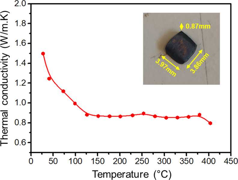
Thermal conductivity of the Pb1–xTe bulk material.
The other members of the IV–VI telluride series, SnTe and GeTe, always form with cation vacancies.34,35 This leads to a high carrier concentration and electrical conductivity, modest Seebeck coefficient, and high thermal conductivity. Therefore, doping is needed to suppress the carrier concentration in order to obtain optimal thermoelectric properties. Stoichiometric PbTe is different in that doping is required to increase the carrier concentration to its optimal value for thermoelectric applications. Our demonstration that stable Pb1–xTe can be obtained by rapid quenching opens the possibility of optimizing the electrical conductivity and Seebeck coefficient without the need for a dopant, thus adding cooling rate to the parameters available for tuning the thermoelectric properties. The next step will be to study the thermoelectric performance of nonstoichiometric Pb1–xTe and also to investigate the possible effect of cooling rate on the microstructure of bulk samples, which can strongly influence the thermal conductivity.
4. Conclusions
Single-crystal and polycrystalline samples of nonstoichiometric Pb1–xTe have been obtained by rapid quenching from the melt. All samples retain the face-centered cubic rock salt structure of stoichiometric PbTe. The morphology of the samples depends on local compositional and solidification conditions inside the quartz tube during quenching. Small single crystals are formed by solidification from the vapor phase and exhibit {100} facets, often not ideally flat due to a variation of local supersaturation via the Berg effect. Hemispherical single crystals and the bulk polycrystalline material are formed by solidification of the liquid phase and contain traces of the Te-rich eutectic phase. In all cases, the quenched materials contain ∼60 at. % Te. We also show that EBSD is an effective method to determine the crystallographic orientation of small crystals. The stabilization of nonstoichiometric Pb1–xTe provides another parameter, the Pb/Te ratio, that gives further scope for the optimization of lead telluride-based thermoelectric materials.
Acknowledgments
H.L. acknowledges financial support from the China Scholarship Council.
Supporting Information Available
The Supporting Information is available free of charge at https://pubs.acs.org/doi/10.1021/acsami.0c20016.
SE image of a cleaved single crystal, SEM-BSE image of the flat surface of an annealed hemispherical crystal, and Pb- and Te-EDS elemental maps showing the presence of Pb-rich rod-shaped branches on the main dendrites (PDF)
The authors declare no competing financial interest.
Supplementary Material
References
- Ioffe F.Semiconductor Thermoelements and Thermoelectric Refrigeration; Infosearch: London, 1957. [Google Scholar]
- Heikes R. R.; Ure R. W.. Thermoelectricity: Science and Engineering; Interscience Publishers, 1961. [Google Scholar]
- Fritts R. W.Thermoelectric Materials and Devices; Reinhold: New York, 1960. [Google Scholar]
- Feit Z.; Kostyk D.; Woods R. J.; Mak P. Single-mode molecular beam epitaxy grown PbEuSeTe/PbTe buried-heterostructure diode lasers for CO2 high-resolution spectroscopy. Appl. Phys. Lett. 1991, 58, 343–345. 10.1063/1.104652. [DOI] [Google Scholar]
- Biswas K.; He J.; Blum I. D.; Wu C.-I.; Hogan T. P.; Seidman D. N.; Dravid V. P.; Kanatzidis M. G. High-performance bulk thermoelectrics with all-scale hierarchical architectures. Nature 2012, 489, 414–418. 10.1038/nature11439. [DOI] [PubMed] [Google Scholar]
- Wu Y.; Nan P.; Chen Z.; Zeng Z.; Liu R.; Dong H.; Xie L.; Xiao Y.; Chen Z.; Gu H.; Li W.; Chen Y.; Ge B.; Pei Y. Thermoelectric enhancements in PbTe alloys due to dislocation-induced strains and converged bands. Adv. Sci. 2020, 7, 1902628. 10.1002/advs.201902628. [DOI] [PMC free article] [PubMed] [Google Scholar]
- Chen T.; Zhang K.; Wang H.; Su W.; Mehmood F.; Wang T.; Zhai J.; Wang X.; Huo T.; Wang C. The high thermoelectric performance of slightly Sb doped PbTe alloys. J. Mater. Chem. C 2020, 8, 1679–1685. 10.1039/c9tc06124j. [DOI] [Google Scholar]
- You L.; Zhang J.; Pan S.; Jiang Y.; Wang K.; Yang J.; Pei Y.; Zhu Q.; Agne M. T.; Snyder G. J.; Ren Z.; Zhang W.; Luo J. Realization of higher thermoelectric performance by dynamic doping of copper in n-type PbTe. Energy Environ. Sci. 2019, 12, 3089–3098. 10.1039/c9ee01137d. [DOI] [Google Scholar]
- Male J.; Agne M. T.; Goyal A.; Anand S.; Witting I. T.; Stevanović V.; Snyder G. J. The importance of phase equilibrium for doping efficiency: iodine doped PbTe. Mater. Horiz. 2019, 6, 1444–1453. 10.1039/c9mh00294d. [DOI] [PubMed] [Google Scholar]
- Jood P.; Ohta M.; Yamamoto A.; Kanatzidis M. G. Excessively doped PbTe with Ge-induced nanostructures enables high-efficiency thermoelectric modules. Joule 2018, 2, 1339–1355. 10.1016/j.joule.2018.04.025. [DOI] [Google Scholar]
- Xiang B.; Liu J.; Yan J.; Xia M.; Zhang Q.; Chen L.; Li J.; Tan X. Y.; Yan Q.; Wu Y. Local nanostructures enhanced the thermoelectric performance of n-type PbTe. J. Mater. Chem. A 2019, 7, 18458–18467. 10.1039/c9ta06247e. [DOI] [Google Scholar]
- Dong J.; Liu W.; Li H.; Su X.; Tang X.; Uher C. In situ synthesis and thermoelectric properties of PbTe–graphene nanocomposites by utilizing a facile and novel wet chemical method. J. Mater. Chem. A 2013, 1, 12503–12511. 10.1039/c3ta12494k. [DOI] [Google Scholar]
- Xiao F.; Yoo B.; Ryan M. A.; Lee K.-H.; Myung N. V. Electrodeposition of PbTe thin films from acidic nitrate baths. Electrochim. Acta 2006, 52, 1101–1107. 10.1016/j.electacta.2006.06.044. [DOI] [Google Scholar]
- Kerner R.; Palchik O.; Gedanken A. Sonochemical and microwave-assisted preparations of PbTe and PbSe. A comparative study. Chem. Mater. 2001, 13, 1413–1419. 10.1021/cm001411h. [DOI] [Google Scholar]
- Saloniemi H.; Kanniainen T.; Ritala M.; Leskelä M. Electrodeposition of PbTe thin films. Thin Solid Films 1998, 326, 78–82. 10.1016/s0040-6090(98)00524-0. [DOI] [Google Scholar]
- Qiu X.; Lou Y.; Samia A. C.; Devadoss A.; Burgess J. D.; Dayal S.; Burda C. PbTe nanorods by sonoelectrochemistry. Angew. Chem., Int. Ed. 2005, 44, 5855–5857. 10.1002/anie.200501282. [DOI] [PubMed] [Google Scholar]
- Tong H.; Zhu Y.-J.; Yang L.-X.; Li L.; Zhang L. Lead chalcogenide nanotubes synthesized by biomolecule-assisted self-assembly of nanocrystals at room temperature. Angew. Chem., Int. Ed. 2006, 45, 7739–7742. 10.1002/anie.200602952. [DOI] [PubMed] [Google Scholar]
- Ao L.; Wang L.; Wang W. Observation of phonon modes in PbTe nanocubes prepared by a solvothermal route. Micro Nano Lett. 2012, 7, 621–623. 10.1049/mnl.2012.0357. [DOI] [Google Scholar]
- Fardy M.; Hochbaum A. I.; Goldberger J.; Zhang M. M.; Yang P. Synthesis and thermoelectrical characterization of lead chalcogenide nanowires. Adv. Mater. 2007, 19, 3047–3051. 10.1002/adma.200602674. [DOI] [Google Scholar]
- Zhang L.; Yu J. C.; Mo M.; Wu L.; Kwong K. W.; Li Q. A general in situ hydrothermal rolling-up formation of one-dimensional, single-crystalline lead telluride nanostructures. Small 2005, 1, 349–354. 10.1002/smll.200400062. [DOI] [PubMed] [Google Scholar]
- Yang Y.; Kung S. C.; Taggart D. K.; Xiang C.; Yang F.; Brown M. A.; Kruse T. J.; Hemminger J. C.; Penner R. M. Synthesis of PbTe nanowire arrays using lithographically patterned nanowire electrodeposition. Nano Lett. 2008, 8, 2447–2451. 10.1021/nl801442c. [DOI] [PubMed] [Google Scholar]
- Pussi K.; Barbiellini B.; Ohara K.; Carbo-Argibay E.; Kolen’ko Y. V.; Bansil A.; Kamali S. Structural properties of PbTe quantum dots revealed by high-energy x-ray diffraction. J. Phys.: Condens. Matter 2020, 32, 485401. 10.1088/1361-648x/abaa80. [DOI] [PubMed] [Google Scholar]
- Wang W. Z.; Poudel B.; Wang D. Z.; Ren Z. F. Synthesis of PbTe nanoboxes using a solvothermal technique. Adv. Mater. 2005, 17, 2110–2114. 10.1002/adma.200500514. [DOI] [Google Scholar]
- Lin J. C.; Hsleh K. C.; Sharma R. C.; Chang Y. A. The Pb-Te (lead-tellurium) system. Bull. Alloy Phase Diagrams 1989, 10, 340–347. 10.1007/bf02877589. [DOI] [Google Scholar]
- Glazov V. M.; Poyarkov K. B. InSb-InAs alloys prepared by rapid quenching (106 – 108 K/s). Inorg. Mater. 2000, 36, 991–996. 10.1007/bf02757973. [DOI] [Google Scholar]
- Sheldrick G. M. A short history of SHELX. Acta Crystallogr., Sect. A: Found. Crystallogr. 2008, 64, 112–122. 10.1107/s0108767307043930. [DOI] [PubMed] [Google Scholar]
- Larson A. C.; von Dreele R. B.. Los Alamos National Laboratory LAUR Report, 2004; No. 86-748.
- Noda Y.; Masumoto K.; Ohba S.; Saito Y.; Toriumi K.; Iwata Y.; Shibuya I. Temperature dependence of atomic thermal parameters of lead chalcogenides, PbS, PbSe and PbTe. Acta Crystallogr., Sect. C: Cryst. Struct. Commun. 1987, 43, 1443–1445. 10.1107/s0108270187091509. [DOI] [Google Scholar]
- Berg W. F. Crystal growth from solutions. Proc. R. Soc. London, Ser. A 1938, 164, 79–95. 10.1098/rspa.1938.0006. [DOI] [Google Scholar]
- Sunagawa I. In-situ investigation on growth and dissolution of crystals in aqueous solution. Aquat. Sci. 1993, 55, 347–357. 10.1007/bf00877279. [DOI] [Google Scholar]
- Sen A.; Ganguly B. Is dual morphology of rock-salt crystals possible with a single additive? The answer is yes, with barbituric acid. Angew. Chem., Int. Ed. 2012, 124, 11441–11445. 10.1002/ange.201206170. [DOI] [PubMed] [Google Scholar]
- Klimakow A. M.; Höfer C. Shaped crystal growth of PbTe by the open tube technique. Cryst. Res. Technol. 1984, 19, 1433–1441. 10.1002/crat.2170191106. [DOI] [Google Scholar]
- Ovsyannikov S. V.; Shchennikov V. V.; Manakov A. Y.; Likhacheva A. Y.; Berger I. F.; Ancharov A. I.; Sheromov M. A. High-pressure X-ray diffraction study of ternary and non-stoichiometric PbTe and PbSe crystals. Phys. Status Solidi B 2007, 244, 279–284. 10.1002/pssb.200672565. [DOI] [Google Scholar]
- Bauer Pereira P.; Sergueev I.; Gorsse S.; Dadda J.; Müller E.; Hermann R. P. Lattice dynamics and structure of GeTe, SnTe and PbTe. Phys. Status Solidi B 2013, 250, 1300–1307. 10.1002/pssb.201248412. [DOI] [Google Scholar]
- Perumal S.; Roychowdhury S.; Biswas K. High performance thermoelectric materials and devices based on GeTe. J. Mater. Chem. C 2016, 4, 7520–7536. 10.1039/c6tc02501c. [DOI] [Google Scholar]
Associated Data
This section collects any data citations, data availability statements, or supplementary materials included in this article.