

Abstract

Hot-electron dynamics taking place in nanostructured materials upon irradiation with fs-laser pulses has been the subject of intensive research, leading to the emerging field of ultrafast nanophotonics. However, the most common description of nonlinear interaction with ultrashort laser pulses assumes a homogeneous spatial distribution for the photogenerated carriers. Here we theoretically show that the inhomogeneous evolution of the hot carriers at the nanoscale can disclose unprecedented opportunities for ultrafast diffraction management. In particular, we design a highly symmetric plasmonic metagrating capable of a transient symmetry breaking driven by hot electrons. The subsequent power imbalance between symmetrical diffraction orders is calculated to exceed 20% under moderate (∼2 mJ/cm2) laser fluence. Our theoretical investigation also indicates that the recovery time of the symmetric configuration can be controlled by tuning the geometry of the metaatom, and can be as fast as 2 ps for electrically connected configurations.
Keywords: Reconfigurable metasurfaces, ultrafast nanophotonics, diffraction management, hot electrons, all-optical modulation
The all-optical manipulation of light is a major challenge of research in optics that has attracted a huge attention for many years, mostly because of the potential to achieve ultrafast modulation speeds. The advent of nanophotonics has opened a new avenue with prospects of outstanding advancements in the field. In particular, optical metasurfaces, that is, engineered two-dimensional metamaterials,1−3 have been demonstrated to provide novel functionalities in flat optics configurations thanks to the control of light at the nanoscale.4−10 Most interestingly, optical metasurfaces can strongly enhance nonlinear effects and make it possible to reconfigure the optical response of the structure using ultrashort laser pulses.11−15 In this respect, plasmonic metasurfaces have turned out to be particularly promising because of the giant third-order nonlinearity of noble metals,16−18 which is governed by photogenerated hot carriers.19−22 The latter have been typically described in terms of a homogeneous distribution in space (see, e.g., ref (15) and references therein), and the effects linked to spatial local inhomogeneities have been overlooked until only very recently.23−26
Among other functionalities, the engineering of optical diffraction with metasurfaces has been widely investigated by exploiting gradient metasurfaces27−31 or metagrating design.32−34 Most recently, electrically reconfigurable metagratings have been also proposed.35
Here we report a theoretical study on a novel approach to reconfigure light diffraction by exploiting hot-electron spatiotemporal dynamics (and related giant optical nonlinearity) in plasmonic nanostructures excited with fs-laser pulses. A suitable quantitative model has been developed to predict a photoinduced spatial asymmetry in plasmonic metagratings with highly symmetric metaatoms, resulting in a transient breaking of the degeneracy of otherwise equivalent diffraction orders. We show that an imbalance as high as 20% between the intensities of the +1 and −1 reflection or transmission orders can be achieved under moderate laser fluence (2 mJ/cm2). Moreover, the recovery time of the symmetric state, and thus the return to balanced scattering, can be readily engineered by acting on the metaatom configuration, and in particular on its topology. Our full-wave simulations indicate that a full return to zero of the all-optical modulation is ultimately limited by the spatial diffusion and subsequent homogenization of the hot carriers within the individual metaatoms. As such, it can be made as fast as ∼2 ps in simply connected configurations, thus overcoming the electron–phonon thermalization bottleneck that typically affects more conventional all-optical modulation schemes based on hot-electron dynamics.
To attain ultrafast diffraction reconfiguration, we first designed a two-dimensional metaatom with the following characteristics: (i) left–right inversion symmetry to guarantee perfect degeneracy of the symmetric (here +1 and −1) steady-state diffraction orders in array configuration and (ii) high sensitivity of the far-field radiation pattern to the breaking of the left–right inversion symmetry to enable diffraction management. When resorting to plasmonic structures, a relatively simple configuration leading to these features is represented by the L-shaped metal nanostrip dimer of Figure 1a. The individual nanostrips (monomers) are well-known to behave as optical nanonantennas,36 exhibiting, under p-polarized plane wave illumination, two distinct resonances in the extinction spectrum: a longitudinal dipolar resonance, for incident electric field parallel to the major axis of the nanostrip, and a transverse dipolar resonance, when the electric field is orthogonal to this axis. For a single gold nanostrip of width W = 165 nm and thickness H = 22.5 nm, embedded in a homogeneous medium with permittivity εeff = 1.522 (i.e., in-between the permittivity of air, 1, and that of a typical glass, ∼2.05), the longitudinal resonance is at around 720 nm (red curve in Figure 1b), whereas the transverse resonance sits around 490 nm (blue curve in Figure 1b).
Figure 1.

Design of the dimeric metaatom. (a) Sketch of the 2D dimeric nanostrip metaatom in a free-standing configuration. The vertices of the nanostrip contours in the xz-plane have been rounded with r = 10 nm radius of curvature to avoid lighting rod effects and artifacts. Numerical analysis details are reported in Supporting Section 1. (b) Extinction cross-section of the nanostrip monomer under plane wave illumination with electric field parallel (red curve) or orthogonal (blue curve) to the nanostrip major axis is compared with the extinction cross-section of the nanostrip dimer with gap g = 8 nm (cf. panel a) excited with electric field aligned to the dimer major axis, that is, x-axis in panel a (green curve). (c) Hybridization scheme of the plasmonic resonances in the plasmonic metaatom under normal incidence (see also Supporting Section 2 for further details). (d) Far-field scattering intensity pattern of the metaatom dimer at the two resonance extinction peaks, corresponding to λEQ = 575 nm (blue and cyan traces) and λED = 930 nm (red traces). The pattern is normalized to the intensity scattered at 90° at λED. Steady-state patterns (solid curves) are compared with out-of-equilibrium patterns (dotted curves) generated after unitary permittivity perturbation is applied to the left nanostrip, mimicking light-induced symmetry breaking following irradiation with intense laser beams impinging at 45° angle of incidence (see inset). Effects of permittivity change with positive sign, Δε = +1 (dotted blue), are compared with the case of negative sign variation, Δε = −1 (dotted cyan). Dashed lines highlight the two scattering directions providing the largest sensitivity of the diffracted intensity to such symmetry breaking.
The extinction cross-section of the nanostrip dimer
(green curve
in Figure 1b) thus
exhibits two distinct resonances, caused by the hybridization of the
two cross-polarized electric dipoles of the nanostrip monomers (Figure 1c). It should be
noted that, for symmetry reasons, under p-polarized
incident plane wave with electric field aligned to the x-axis, only the bonding modes (in which the two dipolar individual
plasmons oscillate in phase one with the other) can be excited. These
correspond to a low energy resonance peaked at around 930 nm, having
an electric dipolar (ED) character (see the characteristic far field
pattern of Figure 1d, solid red trace) and a higher energy resonance at 575 nm. Interestingly,
the latter exhibits an electric quadrupolar (EQ) far-field radiation
pattern (solid blue trace in Figure 1d) that is very sensitive to the breaking of the left–right
inversion symmetry of the metaatom. To illustrate this effect, we
applied a unitary permittivity change Δε (in line with
the order of magnitude of permittivity modulation induced in thin
gold structures under excitation with 100 fs laser pulses at mJ/cm2 fluence level37) only to the left
arm of the dimer and recomputed the far-field radiation patterns.
These are shown as dotted curves in Figure 1d. Note that, in contrast to the dipolar
response at 930 nm, which is almost unchanged, a major distortion
of the quadrupolar pattern at around 575 nm is achieved (compare solid
blue and dotted blue and cyan curves in Figure 1d). Note also that for Δε = +1
(dotted blue), light scattering is on average enhanced in the first
quadrant (0–90°) and depressed in the second quadrant
(90–180°), compared to the static pattern (solid blue),
whereas the opposite behavior is observed under negative sign permittivity
change, Δε = −1 (dotted cyan). The largest change
in the scattering intensity of the nanostrip dimer, of the order of
20%, is achieved at around ±33° from the normal to the dimer
axis (marked by dashed lines in Figure 1d). Therefore, according to the metagrating paradigm,33,34 an array of free-standing plasmonic metaatoms (i.e., embedded in
a homogeneous environment) with pitch a = 855 nm
is expected to inherit the same kind of sensitivity to left–right
symmetry breaking in the m = ± 1 reflection
orders, obeying the grating equation 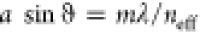 , precisely for
ϑ = ± 33°
at λ = λEQ = 575 nm (
, precisely for
ϑ = ± 33°
at λ = λEQ = 575 nm ( as in Figure 1a).
With these guidelines at hand, and with the aim of addressing real-world applications enabled by a flat-optics large-area configuration,1−3,5−7 we designed the plasmonic metagrating of Figure 2a, made of a 1D array of Au nanostrip dimers. To make our study more realistic, instead of a free-standing metagrating, we assumed a sawtooth molded CaF2 dielectric substrate (with refractive index 1.43) supporting the metallic nanostrips. The array pitch was optimized to address the effects induced by the asymmetric environment and, in the wavelength range of interest, we found optimized sensitivity of the diffraction orders to symmetry breaking for a = 800 nm. The optical response of the structure under p-polarized plane wave excitation at normal incidence (electric field aligned with the x-axis) exhibits a pronounced dip in the zero-order transmission spectrum at around 580 nm wavelength (blue curve in Figure 2b). This is ascribable to the extinction of the EQ resonance of the nanostrip dimer metaatom (Figure 1b), as discussed earlier. The structure also exhibits higher diffraction orders, and in particular the +1 and −1 orders, both in transmission and reflection, as detailed in Figure 2c. Importantly, the two ±1 reflection (transmission) orders are degenerate at normal incidence and excited with the same intensity as long as left–right optical symmetry is satisfied.
Figure 2.

Plasmonic metagrating design. (a) Sketch of the plasmonic metagrating, consisting of a 1D array of cross-polarized Au-nanostrip metaatom dimers on a sawtooth molded dielectric (CaF2) substrate. Linearly p-polarized plane wave illumination at normal incidence is assumed. Inset shows the unit cell defined for 2D simulations: note the left–right inversion symmetry of the unit cell. (b, c) Static optical response of the array in terms of (b) absorption and zero order of reflection and transmission and (c) first (+1 and −1) diffraction orders. Note that, due to unit cell symmetry, +1 and −1 orders are excited with equal amplitude under normal incidence.
Here, we propose an all-optical modulation scheme enabling a dynamical breaking of this symmetry (Figure 3a). The metaatoms are illuminated by an ultrashort laser pulse, referred to as the control pulse, p-polarized and impinging at an angle of 45° with respect to the normal. Under these conditions, one of the arms in the metaatom is directly exposed to the incoming light, whereas the other arm is shaded from radiation. Light absorption thus mostly takes place in the nanostrip monomer exposed to radiation and is much less effective in the other nanostrip. As a result, the spatial distribution of electromagnetic power density across the dimeric metaatom is highly inhomogeneous (see inset in Figure 3a) due to the nonuniform pattern of the near fields within the plasmonic structure. We thus need to define the absorbed power density Pabs(r⃗,t) as a space- and time-dependent variable, assigned locally and changing in time throughout the photoexcitation. Its expression (for not too high fluence, enabling one to disregard nonlinear interactions within the control pulse) can be written as
| 1 |
where the spatial information is enclosed in A(r⃗), representing the inhomogeneous normalized absorption pattern of the control pulse across the photoexcited metaatom, while its temporal evolution is given by the normalized Gaussian intensity profile,
with duration Δt, peaked at time t0. In the equation above, F is the fluence of the control pulse and S is the cross-sectional area of the plasmonic metaatom (in the xz-plane).
Figure 3.

Photoinduced symmetry-breaking
and diffraction management. (a)
Sketch of the all-optical modulation scheme. The p-polarized control pulse at 600 nm wavelength impinges at 45°
angle of incidence and generates a highly inhomogeneous and transient
absorption pattern  (here depicted at time delay τ =
50 fs). (b) First-order transient reflection spectra R±1(τ) at τ = 100 fs time delay (dashed
lines) after control pulse absorption, compared with static (and degenerate)
reflection spectra R±10 (solid lines). (c) Same as in panel
b for transmission orders. (d) Spectra of the DR figure of merit for optical symmetry breaking
in reflection, at different delays τ. (e) Same as panel d for
transmission DT figure
of merit.
(here depicted at time delay τ =
50 fs). (b) First-order transient reflection spectra R±1(τ) at τ = 100 fs time delay (dashed
lines) after control pulse absorption, compared with static (and degenerate)
reflection spectra R±10 (solid lines). (c) Same as in panel
b for transmission orders. (d) Spectra of the DR figure of merit for optical symmetry breaking
in reflection, at different delays τ. (e) Same as panel d for
transmission DT figure
of merit.
This expression for the absorbed power density represents the source term in a set of coupled partial differential equations, in the inhomogeneous version of the so-called three-temperature model (3TM),38,39 here referred to as the I3TM:
| 2 |
| 3 |
| 4 |
The equations above (refer to the Supporting Information, Section 3 for further details) provide a semiclassical description of the spatiotemporal dynamics of out-of-equilibrium noble metal structures in terms of three energy degrees of freedom: N(r⃗,t), the excess energy density stored in the population of nonthermal electrons, directly generated by the absorbed photons; Θe(r⃗,t), the temperature of the population of thermal hot electrons, generated by the relaxation of the nonthermal population via electron–electron scattering; Θl(r⃗,t) the lattice temperature of the metal, which increases via electron–phonon scattering involving both nonthermal and thermal electronic populations. Note that the homogeneous 3TM, originally introduced by Sun and co-workers,38 has been widely used and extensively validated for metallic39 (and semiconduting40) nanosystems upon ultrashort laser pulse illumination, whereas the inhomogeneous version considered in our work has been so far almost overlooked, with the exception of a few recent papers.25,26
For an inhomogeneous excitation, the spatial pattern of N(r⃗,t) becomes inhomogeneous with Θe(r⃗,t) and Θl(r⃗,t) evolving in time and space as in a diffusion process. The excitations represent a spatiotemporal perturbation of the permittivity of gold via the third-order nonlinearity of noble metals, as described in the literature (see, e.g., refs (38 and 39) and references therein). Briefly, pulse absorption results in a modulation of the electronic occupation number in the conduction band, which is detailed by N and Θe. As a consequence, interband transitions are modulated, and a modification of the absorption coefficient, or equivalently of the permittivity imaginary part Δε″, is then straightforwardly computed following a semiclassical approach.39,41 The corresponding real part Δε′ is obtained via Kramers–Kronig analysis. The quantities of Θe and Θl directly influence both the plasma frequency42 and Drude damping43−46 and hence the intraband permittivity. The total (interband and intraband) contributions to the permittivity arising from N, Θe, and Θl then result in a modulation of the gold permittivity Δε(N(r⃗,t), Θe(r⃗,t),Θl(r⃗,t)) = Δε(r⃗,λ,t), constituting an optically induced perturbation.
Such a permittivity modulation can then be experienced by a subsequent weak probe pulse, referred to as the signal pulse, impinging at normal incidence with delay τ with respect to the control pulse. The reflection and transmission orders for the signal pulse are thus expected to evolve over the same time scale as N, Θe, and Θl. Results of the numerical calculations are reported in Figure 3 for realistic values of the control pulse fluence, F = 2 mJ/cm2, and duration (full width at half-maximum in intensity), Δt = 50 fs, readily achievable in pump–probe experiments. It is worth pointing out that, despite the angled excitation of the control pulse, if a homogeneous interaction is assumed, the resulting photoinduced optical perturbation would preserve the x-symmetry of the unit cell. In this framework, higher diffraction orders would be modified relative to the steady-state condition, yet remaining strictly degenerate for symmetry reasons. On the contrary, the highly inhomogeneous pattern for Δε causes a sizable lift of the degeneracy between the +1 and −1 reflection orders, with the dynamical R+1(λ,τ) and R–1(λ,τ) reflection spectra departing from the degenerate R±10(λ) spectrum right after the absorption of the control pulse (Figure 3b). The transmission orders, T+1(λ,τ) and T–1(λ,τ), exhibit a similar dynamic behavior (Figure 3c).
To quantify the optically induced transient imbalance between the ±1 diffraction orders, we define the following metric:
| 5 |
The DT(λ,τ) metric is similarly defined for the imbalance of the ±1 transmission orders.
Transient figure of merit spectra are shown in Figure 3d and e for different values of the control-signal delay time. The DR (DT) is zero in static conditions (i.e., for τ = 0) and increases up to ∼20% right after the absorption of the control pulse, for example, at around τ = 100 fs (dashed curve in Figure 3d,e). The recovery of the degenerate configuration, both in reflection and in transmission, is found to take place in a few tens of ps. Note also that DR exhibits a contrast reversal across the considered range of wavelengths, with negative peak at around 500 nm and positive peak at ∼605 nm (dashed curve in Figure 3d). This reversal is in line with the results of Figure 1d, where we have estimated the effects of opposite sign changes of gold permittivity on the diffraction pattern of the metaatom at the quadrupolar resonance. Indeed, when moving from shorter to longer wavelengths in the considered spectral range, the photoinduced permittivity modulation exhibits a sign change in its real part, from negative to positive, around 550 nm at the initial steps of the dynamics (Figure S2). Also, note that the peaks of DR and DT are retrieved at different wavelengths, and a complete contrast reversal in transmission is observed when tuning the wavelength from ∼600 nm to ∼670 nm (Figure 3e). This misalignment of spectra between the two metrics indicates that the considered transient imbalance cannot be explained as a simple power redistribution between reflection and transmission from ±1 orders. In fact, during the all-optical modulation, extra channels are activated for the interaction of the signal pulse with the dynamical metagrating, which are the modulation of direct transmission (ΔT0) and reflection (ΔR0) orders, as well as transient absorption losses (ΔA), as detailed in Figure S3.
To deepen
our understanding of the mechanisms determining the recovery
of the metaatom symmetry, we analyzed the spatial distribution of
the transient hot electrons temperature,  (Figure 4a). Note that the large electronic thermal
conductivity
of gold results in an ultrafast homogenization of the temperature
field within the individual nanostrips. The bottleneck for an ultrafast
recovery of a symmetric configuration is clearly the nanogap between
the nearby metaatoms, resulting in a large temperature difference
between the two nanostrips.
(Figure 4a). Note that the large electronic thermal
conductivity
of gold results in an ultrafast homogenization of the temperature
field within the individual nanostrips. The bottleneck for an ultrafast
recovery of a symmetric configuration is clearly the nanogap between
the nearby metaatoms, resulting in a large temperature difference
between the two nanostrips.
Figure 4.

Hot electron spatial diffusion. Spatial distribution of the electronic temperature increase ΔΘe in the (a) disconnected dimer nanostrip and the (b) connected geometry variant of the metaatom, at three different control-signal delays. (c) Temporal dynamics of hot carriers temperature variation, shown in two exemplary points (refer to the panel insets) of both the disconnected (dashed lines) and connected (solid lines) structures.
We, therefore, investigated a variation of the geometry where the two nanostrips are connected. Such a topological modification has almost negligible effects on the static optical response (see Supporting Information, section 4) but enables a complete homogenization of the hot electron temperature in the whole metaatom in about 2 ps (Figure 4b), a dramatic improvement compared to the original disconnected configuration (Figure 4c). In the connected geometry, electronic diffusion, governed locally by eq 3, is possible, and energy can readily flow from the more excited arm to the one less exposed to the control pulse illumination. Note that, although homogeneous, Θe is still very high (∼2300 K) at τ = 2 ps (cf. Figure 4b), and the system is thus strongly out of equilibrium (see also Supporting Section 3.3).
Since the imbalance of the diffraction orders is dictated by the symmetry breaking, any symmetric perturbation would leave DR = DT = 0. A substantial speed-up of the return to balanced diffraction is thus predicted in the connected configuration. To verify this, we performed transient optical simulations for the plasmonic metagrating with connected nanostrip metaatoms, following the same procedure described above for the disconnected geometry. A side-by-side comparison of DR(λ,τ) for the two structures is shown in Figure 5a and b. The connected structure (Figure 5b) returns to the symmetric configuration much faster (∼2 ps) than when the gap is present (Figure 5a), where some tens of ps are needed for complete recovery (cf. Figure 3d, dotted trace). Interestingly, similar results hold in transmission (Figures 5c,d), with a slightly more pronounced excursion for the DT metric in the connected configuration (Figure 5d), compared to the DR (see Figure 5b as well as Supporting Section 5). Finally, note the very different dynamics of the transient signal in the disconnected (Figure 5e) and connected (Figure 5f) configurations. On the short time scale of few ps, the disconnected configuration exhibits two distinct peaks, at around 100 fs and 3 ps, respectively. These peaks well correlate with the two contributions to the transient symmetry breaking arising from nonthermal and thermal electrons, respectively (dashed curves in Figure S6a,b). Such an interplay is at work also in the connected configuration, but the contribution from thermal carriers is much weaker and short-lived (solid curves in Figure S6a,b).
Figure 5.

Ultrafast symmetry recovery driven by electronic diffusion. Maps of DR(λ,τ) for the (a) disconnected and (b) connected nanostrip metaatom configurations as a function of the signal wavelength λ and time delay τ. (c, d) Same as in panels a and b for the DT(λ,τ) figure of merit. (e) Time section of the DT map evaluated at the peak wavelength of λ = 590 nm for the disconnected structure. (f) Same as in panel e for the connected structure.
This behavior can be explained as follows. For both structures, the recovery of the original symmetry in the metaatom is conditioned by the equilibration of temperatures between left and right nanostrips. In the connected configuration, this is fully achieved via ultrafast electron diffusion, whose dynamics is dictated by the high photoinduced temperature gradients and the high thermal conductivity of the metal. Conversely, in the disconnected configuration, electron diffusion is inhibited by the gap between the two nanostrips. One thus needs to wait until the much slower electron–phonon relaxation process, taking place on the time scale of few tens of ps, has dissipated all the electron excess energy into lattice heat. Moreover, due to the long-lasting asymmetry in the electron temperatures, lattice heating in the disconnected configuration turns out to be asymmetric as well (compare dashed and solid curves in Figure S6c). This prevents the full closing of the optical symmetry-breaking window induced by the control pulse even after the onset of electron–lattice equilibration. With its ultrafast relaxation to a symmetric state, the electrically connected structure could serve as an ultrafast device, that is, switch, with unprecedented speed, thanks to the rejection of electron–phonon and phonon–phonon relaxation bottlenecks that are typical of other all-optical modulation schemes. However, cumulative thermal heating in the lattice and the substrate, following repetitive absorption of several control pulses at a high repetition rate, can nevertheless induce a contrast reduction in the DR and DT signals that ought to be addressed to enable real-world operation of the device. This could be done, for example, by employing, for the dielectric substrate, materials having higher thermal conductivity like BeO, as suggested in ref (12).
In conclusion, we have introduced a novel approach for all-optical light management, the dynamic spatiotemporal modulation of plasmon-induced hot carriers. A plasmonic metagrating with highly symmetric metaatoms supporting degenerate ±1 diffraction orders has been designed. The excitation using fs-laser pulses is theoretically predicted to induce a highly nonuniform permittivity modulation in the individual metaatoms. This results in a transient symmetry breaking of their diffraction pattern and an imbalance of their ±1 diffraction orders exceeding 20% under moderate fluence (∼2 mJ/cm2) of the control pulse. Since the dynamics of the optical symmetry breaking is governed by the hot-electrons temperature homogenization within the individual metaatoms, the photoinduced symmetry breaking can be controlled by tuning the geometry. We found that an electrically connected configuration of the metaatom enables a substantial speed-up of the return to balanced diffraction, taking place in about 2 ps. Our theoretical results provide a novel approach for reconfigurable metasurface engineering with unprecedented ultrafast switching possibilities, for example, ultrafast dynamical beam splitting. Our findings are also of importance for advancements in hot-electron harvesting applications,47 including the optimization of plasmon-enhanced photocatalysis and photodetection configurations, enabled by a refined design aware of the ultrafast nanoscale inhomogeneities.
Acknowledgments
This publication is part of the METAFAST project that received funding from the European Union Horizon 2020 Research and Innovation programme under Grant Agreement No. 899673. This work reflects only author view and the European Commission is not responsible for any use that may be made of the information it contains. P.N. acknowledges support from the Robert A. Welch Foundation (grant no. C-1222).
Supporting Information Available
The Supporting Information is available free of charge at https://pubs.acs.org/doi/10.1021/acs.nanolett.0c04075.
Design of dimeric metaatom; hybridization scheme validation; ultrafast photoexcitation modeling; optical static response of connected configuration; diffraction management in connected configuration; dynamics of internal degrees of freedom (PDF)
The authors declare no competing financial interest.
Supplementary Material
References
- Kildishev A. V.; Boltasseva A.; Shalaev V. M. Planar Photonics with Metasurfaces. Science 2013, 339, 1289. 10.1126/science.1232009. [DOI] [PubMed] [Google Scholar]
- Neshev D. N.; Aharonovich I. Optical Metasurfaces: New Generation Building Blocks for Multi-Functional Optics. Light: Sci. Appl. 2018, 7, 59. 10.1038/s41377-018-0058-1. [DOI] [PMC free article] [PubMed] [Google Scholar]
- Glybovski S. B.; Tretyakov S. A.; Belov P. A.; Kivshar Y. S.; Simovski C. R. Metasurfaces: from Microwaves to Visible. Phys. Rep. 2016, 634, 1–72. 10.1016/j.physrep.2016.04.004. [DOI] [Google Scholar]
- Aieta F.; Genevet P.; Kats M. A.; Yu N.; Blanchard R.; Gaburro Z.; Capasso F. Aberration-Free Ultrathin Flat Lenses and Axicons at Telecom Wavelength Based on Plasmonic Metasurface. Nano Lett. 2012, 9, 4932–4936. 10.1021/nl302516v. [DOI] [PubMed] [Google Scholar]
- Yu N.; Genevet P.; Aieta F.; Kats M. A.; Blanchard R.; Aoust G.; Tetienne J.-P.; Gaburro Z.; Capasso F. Flat Optics: Controlling Wavefronts with Optical Antenna Metasurfaces. IEEE J. Sel. Top. Quantum Electron. 2013, 19, 4700423. 10.1109/JSTQE.2013.2241399. [DOI] [Google Scholar]
- Yu N.; Capasso F. Flat Optics with Designer Metasurfaces. Nat. Mater. 2014, 13, 139. 10.1038/nmat3839. [DOI] [PubMed] [Google Scholar]
- Chen H.-T.; Taylor A. J.; Yu N. A Review of Metasurfaces: Physics and Application. Rep. Prog. Phys. 2016, 79, 076401 10.1088/0034-4885/79/7/076401. [DOI] [PubMed] [Google Scholar]
- Chong K. E.; Staude I.; James A.; Dominguez J.; Lui S.; Campione S.; Subramania G. S.; Luk T. S.; Decker M.; Neshev; et al. Polarization-Independent Silicon Metadevices for Efficient Optical Wavefront Control. Nano Lett. 2015, 15, 5369–5374. 10.1021/acs.nanolett.5b01752. [DOI] [PubMed] [Google Scholar]
- Shalaev M. I.; Sun J.; Tsukernik A.; Pandey A.; Nikolskiy K.; Litchinitser N. M. High-Efficiency All-Dielectric Metasurfaces for Ultracompact Beam Manipulation in Transmission Mode. Nano Lett. 2015, 15, 6261–6266. 10.1021/acs.nanolett.5b02926. [DOI] [PubMed] [Google Scholar]
- Wang K.; Titchener J. G.; Kruk S. S.; Xu L.; Chung H.-P.; Parry M.; Kravchenko I. I.; Chen Y.-H.; Solntsev A. S.; Kivshar Y. S.; et al. Quantum Metasurface for Multiphoton Interference and State Reconstruction. Science 2018, 361, 1104. 10.1126/science.aat8196. [DOI] [PubMed] [Google Scholar]
- Yang Y.; Wang W.; Boulesbaa A.; Kravchenko I. I.; Briggs D. P.; Puretzky A.; Geohegan D.; Valentine J. Nonlinear Fano-Resonant Dielectric Metasurfaces. Nano Lett. 2015, 15, 7388–7393. 10.1021/acs.nanolett.5b02802. [DOI] [PubMed] [Google Scholar]
- Shcherbakov M. R.; Vabishchevich P. P.; Shorokhov A. S.; Chong K. E.; Choi D.-Y.; Staude I.; Miroshnichenko A. E.; Neshev D. N.; Fedyanin A. A.; Kivshar Y. Ultrafast All-Optical Switching with Magnetic Resonances in Nonlinear Dielectric Nanostructures. Nano Lett. 2015, 15, 6985–6990. 10.1021/acs.nanolett.5b02989. [DOI] [PubMed] [Google Scholar]
- Liu S.; Sinclair M. B.; Saravi S.; Keeler G. A.; Yang Y.; Reno J.; Peake G. M.; Setzpfandt F.; Staude I.; Pertsch T.; Brener I. Resonantly Enhanced Second-Harmonic Generation Using III-V Semiconductor All-Dielectric Metasurfaces. Nano Lett. 2016, 16, 5426–5432. 10.1021/acs.nanolett.6b01816. [DOI] [PubMed] [Google Scholar]
- Della Valle G.; Hopkins B.; Ganzer L.; Stoll T.; Rahmani M.; Longhi S.; Kivshar Y. S.; De Angelis C.; Neshev D. N.; Cerullo G. Nonlinear Anisotropic Dielectric Metasurfaces for Ultrafast Nanophotonics. ACS Photonics 2017, 4, 2129–2136. 10.1021/acsphotonics.7b00544. [DOI] [Google Scholar]
- Ren M.; Cai W.; Xu J. Tailorable Dynamics in Nonlinear Optical Metasurfaces. Adv. Mater. 2020, 32, 1806317. 10.1002/adma.201806317. [DOI] [PubMed] [Google Scholar]
- Wurtz G. A.; Pollard R.; Hendren W.; Wiederrecht G. P.; Gosztola D. J.; Podolskiy V. A.; Zayats A. V. Designed Ultrafast Optical Nonlinearity in a Plasmonic Nanorod Metamaterial Enhanced by Nonlocality. Nat. Nanotechnol. 2011, 6, 107–111. 10.1038/nnano.2010.278. [DOI] [PubMed] [Google Scholar]
- Kauranen M.; Zayats A. V. Nonlinear Plasmonics. Nat. Photonics 2012, 6, 737. 10.1038/nphoton.2012.244. [DOI] [Google Scholar]
- Conforti M.; Della Valle G. Derivation of Third-Order Nonlinear Susceptibility of Thin Metal Films as a Delayed Optical Response. Phys. Rev. B: Condens. Matter Mater. Phys. 2012, 85, 245423. 10.1103/PhysRevB.85.245423. [DOI] [Google Scholar]
- Brongersma M.; Halas N. J.; Nordlander P. Plasmon-Induced Hot Carrier Science and Technology. Nat. Nanotechnol. 2015, 10, 25–34. 10.1038/nnano.2014.311. [DOI] [PubMed] [Google Scholar]
- Liu J. G.; Zhang H.; Link S.; Nordlander P. Relaxation of Plasmon-Induced Hot Carriers. ACS Photonics 2018, 5, 2584–2595. 10.1021/acsphotonics.7b00881. [DOI] [Google Scholar]
- Baida H.; Mongin D.; Christofilos D.; Bachelier G.; Crut A.; Maioli P.; Del Fatti N.; Vallée F. Ultrafast Nonlinear Optical Response of a Single Gold Nanorod near Its Surface Plasmon Resonance. Phys. Rev. Lett. 2011, 107, 057402 10.1103/PhysRevLett.107.057402. [DOI] [PubMed] [Google Scholar]
- Manjavacas A.; Liu J. G.; Kulkarni V.; Nordlander P. Plasmon-Induced Hot Carriers in Metallic Nanoparticles. ACS Nano 2014, 8, 7630. 10.1021/nn502445f. [DOI] [PubMed] [Google Scholar]
- Block A.; Liebel M.; Yu R.; Spector M.; Sivan Y.; García de Abajo F. J.; van Hulst N. F. Tracking Ultrafast Hot-Electron Diffusion in Space and Time by Ultrafast Thermomodulation Microscopy. Sci. Adv. 2019, 5, eaav8965 10.1126/sciadv.aav8965. [DOI] [PMC free article] [PubMed] [Google Scholar]
- Nicholls L. H.; Stefaniuk T.; Nasir M. E.; Rodríguez-Fortuño F. J.; Wurtz G. A.; Zayats A. V. Designer Photonic Dynamics by Using Non-Uniform Electron Temperature Distribution for On-Demand All-Optical Switching Times. Nat. Commun. 2019, 10, 2967. 10.1038/s41467-019-10840-7. [DOI] [PMC free article] [PubMed] [Google Scholar]
- Sivan Y.; Spector M. Ultrafast Dynamics of Optically-Induced Heat Gratings in Metals. ACS Photonics 2020, 7, 1271–1279. 10.1021/acsphotonics.0c00224. [DOI] [Google Scholar]
- Schirato A.; Maiuri M.; Toma A.; Fugattini S.; Proietti Zaccaria R.; Laporta P.; Nordlander P.; Cerullo G.; Alabastri A.; Della Valle G. Transient Optical Symmetry Breaking for Ultrafast Broadband Dichroism in Plasmonic Metasurfaces. Nat. Photonics 2020, 14, 723–727. 10.1038/s41566-020-00702-w. [DOI] [Google Scholar]
- Sun S.; Yang K.-Y.; Wang C.-M.; Juan T.-K.; Chen W. T.; Liao C. Y.; He Q.; Xiao S.; Kung W.-T.; Guo G.-Y.; et al. High-Efficiency Broadband Anomalous Reflection by Gradient Metasurfaces. Nano Lett. 2012, 12, 6223–6229. 10.1021/nl3032668. [DOI] [PubMed] [Google Scholar]
- Pors A.; Nielsen M. G.; Eriksen R. L.; Bozhevolnyi S. I. Broadband Focusing Flat Mirrors Based on Plasmonic Gradient Metasurfaces. Nano Lett. 2013, 13, 829–834. 10.1021/nl304761m. [DOI] [PubMed] [Google Scholar]
- Asadchy V. S.; Albooyeh M.; Tcvetkova S. N.; Díaz-Rubio A.; Ra’di Y.; Tretyakov S. A. Perfect Control of Reflection and Refraction Using Spatially Dispersive Metasurfaces. Phys. Rev. B: Condens. Matter Mater. Phys. 2016, 94, 075142 10.1103/PhysRevB.94.075142. [DOI] [Google Scholar]
- Mohammadi Estakhri N.; Alù A. Wavefront Transformation with Gradient Metasurfaces. Phys. Rev. X 2016, 6, 041008 10.1103/PhysRevX.6.041008. [DOI] [Google Scholar]
- Epstein A.; Eleftheriades G. V. Huygens’ Metasurfaces via the Equivalence Principle: Design and Applications. J. Opt. Soc. Am. B 2016, 33, A31–A50. 10.1364/JOSAB.33.000A31. [DOI] [Google Scholar]
- Sell D.; Yang J.; Doshay S.; Yang R.; Fan J. A. Large-Angle Multifunctional Metagratings Based on Freeform Multimode Geometries. Nano Lett. 2017, 17, 3752–3757. 10.1021/acs.nanolett.7b01082. [DOI] [PubMed] [Google Scholar]
- Ra’di Y.; Sounas D. L.; Alù A. Metagratings: Beyond the Limits of Graded Metasurfaces for Wave Front Control. Phys. Rev. Lett. 2017, 119, 067404 10.1103/PhysRevLett.119.067404. [DOI] [PubMed] [Google Scholar]
- Popov V.; Boust F.; Burokur S. N. Controlling Diffraction Patterns with Metagratings. Phys. Rev. Appl. 2018, 10, 011002 10.1103/PhysRevApplied.10.011002. [DOI] [Google Scholar]
- Ra’di Y.; Alù A. Reconfigurable Metagratings. ACS Photonics 2018, 5, 1779–1785. 10.1021/acsphotonics.7b01528. [DOI] [Google Scholar]
- Della Valle G.; Sondergaard T.; Bozhevolnyi S. I. Plasmon-Polariton Nano-Strip Resonators: from Visible to Infra-Red. Opt. Express 2008, 16, 6867. 10.1364/OE.16.006867. [DOI] [PubMed] [Google Scholar]
- Dal Conte S.; Conforti M.; Petti D.; Albisetti E.; Longhi S.; Bertacco R.; De Angelis C.; Cerullo G.; Della Valle G. Disentangling Electrons and Lattice Nonlinear Optical Response in Metal-Dielectric Bragg Filters. Phys. Rev. B: Condens. Matter Mater. Phys. 2014, 89, 125122. 10.1103/PhysRevB.89.125122. [DOI] [Google Scholar]
- Sun C.-K.; Vallée F.; Acioli L. H.; Ippen E. P.; Fujimoto J. G. Femtosecond-Tunable Measurement of Electron Thermalization in Gold. Phys. Rev. B: Condens. Matter Mater. Phys. 1994, 50, 15337. 10.1103/PhysRevB.50.15337. [DOI] [PubMed] [Google Scholar]
- Zavelani-Rossi M.; Polli D.; Kochtcheev S.; Baudrion A.-L.; Béal J.; Kumar V.; Molotokaite E.; Marangoni M.; Longhi S.; Cerullo G.; et al. Transient Optical Response of a Single Gold Nanoantenna: the Role of Plasmon Detuning. ACS Photonics 2015, 2, 521–529. 10.1021/ph5004175. [DOI] [Google Scholar]
- Scotognella F.; Della Valle G.; Kandada A. R. S.; Dorfs D.; Zavelani-Rossi M.; Conforti M.; Miszta K.; Comin A.; Korobchevskaya K.; Lanzani G.; Manna L.; Tassone F. Plasmon Dynamics in Colloidal Cu2–xSe Nanocrystals. Nano Lett. 2011, 11, 4711. 10.1021/nl202390s. [DOI] [PubMed] [Google Scholar]
- Rosei R.; Antonangeli F.; Grassano U. M. d Bands Position and Width in Gold from Very Low Temperature Thermomodulation Measurements. Surf. Sci. 1973, 37, 689. 10.1016/0039-6028(73)90359-2. [DOI] [Google Scholar]
- Yeshchenko O. A.; Bondarchuk I. S.; Gurin V. S.; Dmitruk I. M.; Kotko A. V. Temperature Dependence of the Surface Plasmon Resonance in Gold Nanoparticles. Surf. Sci. 2013, 608, 275. 10.1016/j.susc.2012.10.019. [DOI] [Google Scholar]
- Labouret T.; Palpant B. Nonthermal Model for Ultrafast Laser-Induced Plasma Generation around a Plasmonic Nanorod. Phys. Rev. B: Condens. Matter Mater. Phys. 2016, 94, 245426. 10.1103/PhysRevB.94.245426. [DOI] [Google Scholar]
- Gurzhi R. N. Mutual Electron Correlations in Metal Optics. Sov. Phys. JETP 1959, 35, 673–675. [Google Scholar]
- Tsai C. Y.; Tsai C. Y.; Chen C. H.; Sung T. L.; Wu T. Y.; Shih F. P. Theoretical Model for Intravalley and Intervalley Free-Carrier Absorption in Semiconductor Lasers: beyond the Classical Drude Model. IEEE J. Quantum Electron. 1998, 34, 552–559. 10.1109/3.661466. [DOI] [Google Scholar]
- Smith J. B.; Ehrenreich H. Frequency Dependence of the Optical Relaxation Time in Metals. Phys. Rev. B: Condens. Matter Mater. Phys. 1982, 25, 923. 10.1103/PhysRevB.25.923. [DOI] [Google Scholar]
- Naik G. V.; Dionne J. A. Photon upconversion with hot carriers in plasmonic systems. Appl. Phys. Lett. 2015, 107, 133902. 10.1063/1.4932127. [DOI] [Google Scholar]
Associated Data
This section collects any data citations, data availability statements, or supplementary materials included in this article.