

Abstract

Visible light communications (VLC) require III-nitride visible micro-light-emitting diodes (μLEDs) with a high-modulation bandwidth. Such μLEDs need to be driven at a high injection current density on a kA/cm2 scale, which is about 2 orders of magnitude higher than those for normal visible LED operation. μLEDs are traditionally fabricated by dry-etching techniques where dry-etching-induced damages are unavoidable, leading to both a substantial reduction in performance and a great challenge to viability at a high injection current density. Furthermore, conventional biasing (which is simply applied across a p–n junction) is good enough for normal LED operation but generates a great challenge for a single μLED, which needs to be modulated at a high injection current density and at a high frequency. In this work, we have proposed a concept for an epitaxial integration and then demonstrated a completely different method that allows us to achieve an epitaxial integration of a single μLED with a diameter of 20 μm and an AlGaN/GaN high-electron-mobility transistor (HEMT), where the emission from a single μLED is modulated by tuning the gate voltage of its HEMT. Furthermore, such a direct epitaxial approach has entirely eliminated any dry-etching-induced damages. As a result, we have demonstrated an epitaxial integration of monolithic on-chip μLED-HEMT with a record modulation bandwidth of 1.2 GHz on industry-compatible c-plane substrates.
Keywords: MicroLEDs; modulation bandwidth, GaN; selective overgrowth; HEMTs; VLC
1. Introduction
There is an increasing demand of developing visible light communications (VLC)1,2 as a complementary technology to radio frequency (RF)-based Wi-Fi and 5G, where III-nitride visible light-emitting diodes (LEDs) used as transmitters are the key components.3−7 It is expected that the VLC technology has many applications in a wide range of scenarios where RF emissions are controlled or do not work,8,9 such as hospitals, schools, airplanes, underwater communications, hazardous environments which contain oil, gas, petrochemicals, etc.
Generally speaking, a frequency bandwidth (Δν) is inversely proportional to the square of the wavelength, which is described as below
| 1 |
where λ is the wavelength and c is the speed of light. Consequently, RF emissions span a limited range from 3 kHz to 300 GHz, while the wavelengths of visible light are much shorter than those of RF emissions leading to a huge range from 430 to 750 THz, which is more than 3 orders of magnitude larger than RF. Moreover, VLC presents another unique advantage which Wi-Fi and 5G lack, namely, security-related applications, as visible light propagation can be easily restrained to a confined space without information leakage concerns intrinsic in Wi-Fi or 5G.8,9
One of the greatest challenges the current VLC technology is facing is due to its limited modulation bandwidth, which is far from satisfactory and thus poses an insurmountable barrier for promoting VLC applications. In principle, a modulation bandwidth is determined by the larger of the RC time constant of the junction capacitance and the carrier recombination lifetime of III-nitride visible LEDs used as a transmitter. Considering a blue LED typically used for a VLC system, where an active region consists of InGaN/GaN multiple quantum wells (MQWs) and the thickness of the active regions is typically around 100 nm, the RC time constant can be estimated using a simple equation provided below
| 2 |
where R is the electrical impedance, A is the LED area, L can be roughly estimated as the thickness of an active region, ε is the dielectric constant of GaN which is about 9, and ε0 is the vacuum permittivity.
Equation 2 indicates that the RC time constant reduces with decreasing LED dimension. For example, if the dimension of a LED is reduced from a standard size of 330 × 330 μm2 to 20 μm in diameter, the RC time constant significantly reduces to 0.05 ns from more than 10 ns assuming an electrical impedance of 50 Ω. As a result, the modulation bandwidth (∼1/(2πRC)) can drastically increase to >10 GHz for a micro-LED (μLED) with 20 μm in diameter from 50 MHz for a standard 330 × 330 μm2 LED. This is the fundamental physics why it is essential to employ a μLED as a transmitter for VLC.
It is worth highlighting that the above estimation is valid for the μLED only under a condition that the carrier recombination lifetime of the μLED is shorter than 0.05 ns. However, it is well known that the carrier recombination lifetime of a standard blue LED is typically ≥10 ns under normal operation. Therefore, the modulation bandwidth for VLC applications is mainly dominated by the carrier recombination lifetime of a blue LED instead of its RC time constant. To significantly reduce the carrier recombination lifetime of a blue LED, one of the possible solutions is to drive a blue LED at a substantially high injection current density.10 Therefore, the simplest option is to use a μLED as a transmitter for VLC. However, a μLED with high quality is essential, otherwise, it is extremely difficult to sustain a μLED at a high injection current density, which is typically on an order of kA/cm2 (ref (11)).
Unfortunately, a dry-etching technique remains the main approach for the fabrication of III-nitride μLEDs.10−15 Consequently, dry-etching-induced damages are unavoidable, leading to both a substantial reduction in performance and a great challenge to viability at a high injection current density.16,17 This concern is significantly enhanced with decreasing μLED dimension down to 100 μm, in particular, ≤20 μm.18−20 Recent evidence suggests that μLEDs typically exhibit much lower external quantum efficiency (EQE) than their counterparts with a macro dimension (>100 μm).21,22 This is much more pronounced when the dimension of a μLED is ≤20 μm. Furthermore, although an advanced atomic layer deposition (ALD) technique is adopted for surface passivation, the improvement is marginal.23,24 Therefore, traditional dry-etching processes cannot meet the requirement for the fabrication of III-nitride μLEDs with high performance. This is possibly one of the fundamental reasons why the modulation bandwidth of μLEDs for VLC on industry-compatible c-plane substrates is limited to 1 GHz.
Another issue which is often ignored is due to the electrically driving part for VLC. For standard displays or general illumination, III-nitride LEDs are driven at a low injection current density, typically, ≤10 A/cm2. In this case, the stable operation of a LED can be obtained when a forward bias is simply applied across its p and n layers. In contrast, for VLC applications, a single μLED is normally driven at a high injection current density on an order of kA/cm2 and further needs to be modulated at a high frequency.14,25 In this case, the conventional biasing method may not be good enough.
To overcome this challenge, we are proposing to integrate a μLED and an AlGaN/GaN high-electron-mobility transistor (HEMT) as schematically illustrated in Figure 1, which is also compared with a standard LED modulation. For the conventional biasing method, when a LED needs to be operated at a high injection current density, a tiny change in forward bias will lead to an enormous change in injection current density as shown in Figure 1a, which is very difficult to maintain and control. In contrast, if a HEMT is used to supply injection current to a LED as shown in Figure 1b, the situation is different, as a high injection current density can be stably and easily controlled by simply tuning the gate voltage of its HEMT. However, an immediate question is how to integrate a μLED and a HEMT.
Figure 1.

(a) Conventional biasing method for LED operation and (b) our proposed biasing method for a single μLED operation, where the single μLED is modulated by tuning the gate voltage of its HEMT. The insets are equivalent electrical circuits for these two cases.
To address the great challenges in fabricating μLEDs, very recently we have demonstrated a direct epitaxial approach to achieving ultrasmall μLEDs with a record EQE.26,27 By means of employing a selective overgrowth on predefined microhole arrays formed by SiO2 masks on n-GaN templates, our regularly arrayed μLEDs can naturally form without involving any dry-etching processes. As a consequence, our approach has entirely eliminated any dry-etching-induced damages.
In this work, we are proposing to perform the selective overgrowth of μLEDs on predefined microhole arrays formed by SiO2 masks on an AlGaN/GaN HEMT template, aiming to achieve monolithically integrated HEMT-μLED devices. In our approach, the μLED emission is modulated directly by tuning the gate voltage of its HEMT. By this approach, we have achieved an epitaxial integration of monolithic on-chip μLED-HEMTs on industry-compatible c-plane substrates, where a single μLED with a diameter of 20 μm is controlled by its AlGaN/GaN HEMT. Our monolithically integrated μLED-HEMT device has demonstrated a record modulation bandwidth of 1.2 GHz.
2. Results and Discussion
Figure 2 schematically illustrates our procedure for preparing a microhole array pattern on an AlGaN/GaN HEMT template grown on the c-plane sapphire substrate, where the microhole arrays are for the selective overgrowth of μLEDs. Initially, a layer of SiO2 is deposited on an AlGaN/GaN template on c-plane sapphire (Figure 2a), and then a combination of a standard photolithography technique and then inductive-coupled plasma (ICP) dry-etching process is employed to etch SiO2 into microhole arrays. Afterwards, the HEMT template will be further etched by >50 nm, but the etching only takes place within the microhole regions (using the SiO2 microhole masks). The diameter of the microholes is 20 μm, and the edge-to-edge spacing is 25 μm. Subsequently, the patterned HEMT template is then reloaded into a metalorganic vapor-phase epitaxy (MOVPE) system for further μLED growth. As a result of the SiO2 masks, μLEDs can be grown only within the microhole regions, naturally forming μLED arrays. The μLED structure is fairly standard, consisting of a layer of n-GaN, 30 periods of In0.05Ga0.95N/GaN superlattices (SLs) as a prelayer, 5 periods of In0.25Ga0.75N/GaN MQWs (well: 2.5 nm; barrier: 13 nm) as an active region, a 20 nm p-Al0.20Ga0.80N electron blocking layer, and a final 150 nm p-GaN layer (Figure 2c). It is essential that the overgrown n-GaN of μLEDs within the microhole areas directly contacts the interface between the AlGaN barrier and the GaN buffer of the HEMT so that each single μLED is electrically connected with the HEMT through the two-dimensional electron gases (2DEG) formed at the interface between the AlGaN barrier and the GaN buffer of the HEMT. Finally, all of the SiO2 masks are simply removed using 40% HF acid (Figure 2d).
Figure 2.

Schematics of our procedure for the selective overgrowth of μLEDs on a HEMT template featuring predefined microhole arrays. (a) PECVD depositing SiO2; (b) patterning and then fabricating SiO2 microhole arrays; (c) selective overgrowth of microLEDs; and (d) SiO2 mask removal using HF.
Subsequently, a standard device fabrication process is performed to form metal contacts for both HEMT and μLED, for which please refer to a detailed process flowchart schematically illustrated in Figure S1 in the Supporting Information.
Figure 3a shows a cross-sectional scanning electron microscope (SEM) image of a single μLED with 20 μm in diameter overgrown on the HEMT template. Figure 3b shows the three-dimensional (3D) schematics of our monolithically integrated HEMT and μLED (i.e., a circular gate contact is used) with the inset illustrating the two-dimensional gas (2DEG) formed at the AlGaN/GaN interface of the HEMT epitaxially connecting with the n-GaN of a μLED. This demonstrates that a monolithic on-chip integration of μLED and HEMT can naturally form through epitaxial growth.
Figure 3.

Layout of an epitaxially monolithic on-chip integration of μLED-HEMT. (a) Cross-sectional SEM image of the overgrown epi before device fabrication; (b) three-dimensional schematics of the integrated device after fabrication. The inset schematically illustrates the cross-sectional epi-structure of our monolithically integrated device, where 2DEG is represented by dashed red lines.
Figure 4a shows the optical microscope image of our monolithic on-chip integrated μLED-HEMT with a zoom-in SEM image, demonstrating that the circular gate of a HEMT surrounds a single μLED with 20 μm in diameter. The mesa in a square shape is defined for the whole integrated μLED-HEMT device. Ground-signal-ground (GSG) pads with a center-to-center distance of 100 μm are especially designed for air coplanar (ACP) wafer probes used for our on-wafer high-frequency measurements. Due to our completely different method (i.e., our direct epitaxial selective growth in comparison with conventional dry-etching-based fabrication methods), our μLEDs form naturally, thus entirely eliminating any dry-etching-induced damages, in particular, sidewall damages, which is particularly important for the fabrication of μLEDs with ≤20 μm in diameter as a result of a significant increase in the ratio of surface to volume.
Figure 4.

(a) Optical microscope image of our monolithically integrated device with a zoom-in SEM image; (b) typical I–V characteristics as a function of gate bias (Inset: an equivalent electrical circuit for testing); and (c) typical transfer characteristics.
As shown in Figure 4a, a circular anode pad is fabricated on top of the p-GaN of the single μLED. The regions outside each μLED are the HEMT areas. A circular gate is fabricated around each single μLED, and its length, gate-to-source distance, and gate width are 2, 2, and 88 μm, respectively. The spacing between the gate and the n-GaN of each single μLED is 3 μm. Outside the circular gate regions, two semicircular pads are fabricated as source pads for the HEMT.
Current–voltage (I–V) and transfer characteristics have been performed on our monolithically integrated μLED-HEMT, where the electrical current which is injected into a single μLED is controlled by its HEMT. A two-channel source meter Keithley 2612B has been used for these measurements.
Figure 4b shows the injection current which flows into a single μLED as a function of the applied voltage between the anode of the μLED and the source of its HEMT measured under different gate bias ranging from 1 to −7 V, demonstrating a typical HEMT characteristic. The inset shows an equivalent electrical circuit, schematically illustrating how the HEMT provides injection current to a single μLED, which is controlled by the gate bias of the HEMT. Figure 4b indicates that the highest injection current which the HEMT can provide to a single μLED is 45 mA, which is ∼14.3 kA/cm2, demonstrating that our μLED can sustain at such a high injection current density. In addition, this also confirms the excellent quality of our μLED achieved by our unique approach, where the dry-etching-induced damages which cannot be avoided in conventional fabrication methods are entirely eliminated.
Figure 4c shows a typical transfer characteristic of our monolithically integrated μLED-HEMT, indicating that the HEMT demonstrates an excellent capability of controlling a single μLED.
Subsequently, modulation bandwidth measurements have been performed on our monolithically integrated HEMT-μLED. A single μLED which is probed by two G–S–G RF probes is modulated via the gate terminal of its HEMT with a small AC signal provided by Port 1 of a vector network analyzer (VNA), where a DC bias from a source meter (Keithley 2612B) is added to the AC signal. The EL emission from the single μLED is collected by a light collection system consisting of a 10× objective lens, a collimator, and a 50 cm fiber (please refer to Figure S2 in the Supporting Information), then converted into an electrical signal and amplified by a fiber-coupled photoreceiver, and finally introduced into Port 2 of VNA. The total distance between our μLED and the receiver is around 1 m.
Figure 5a shows the frequency response of our single μLED controlled by its HEMT, namely, the normalized output power as a function of frequency measured under different gate bias of the HEMT. The frequency response measurements have been carried out as a function of injection current density, exhibiting a 3 dB modulation bandwidth of 1.2 GHz at 13.3 kA/cm2 which can be obtained under zero gate bias and 10 V anode with respect to the source of the HEMT. This demonstrates the highest modulation bandwidth reported so far. Table 1 provides the benchmarking of our monolithic on-chip integration of μLED-HEMT against the current state-of-the-art μLEDs on industry-compatible c-plane substrates in terms of 3 dB modulation bandwidth.10,14,28−32
Figure 5.
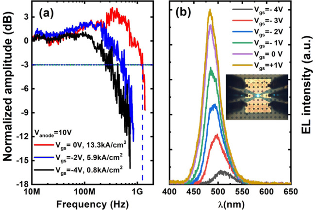
(a) Three decibel modulation bandwidth of our monolithically integrated device as a function of gate bias measured under Vanode = 10 V; (b) EL spectra of our monolithically integrated device measured as a function of gate bias. The inset shows a typical EL emission image taken under Vgs = −4 V and Vanode = 8 V.
Table 1. Benchmarking Our Monolithically Integrated HEMT and μLED Against Current State-of-the-Art μLEDs on Industry-Compatible c-Plane Substrates in Terms of 3 dB Modulation Bandwidth.
Figure 5b presents the electroluminescence (EL) spectra from the single μLED as a function of gate bias that controls injection current into the μLED, showing that the EL peak wavelength shifts from 510 to 480 nm with increasing gate bias. The blue shift in EL peak wavelength is due to an increase in injection current, which suppresses the piezoelectrical field-induced quantum-confined Stark effect (QCSE) as a result of the screening effect. Of course, it is expected that the band-filling effect also contributes to the blue shift at a high injection current.33 A fiber-coupled spectrometer FLAME-S-UV–VIS manufactured by Ocean Optics has been used to perform EL measurements. Figure 5b further confirms that our single μLED can be stably controlled by simply tuning the gate bias of its HEMT, which greatly simplifies the μLED driving circuitry. The inset shows a typical optical image of the EL emission from our single μLED controlled by its HEMT.
3. Conclusions
In conclusion, we have employed our direct epitaxial approach to achieving small μLEDs on predefined microhole arrays formed by SiO2 masks on an AlGaN/GaN HEMT template, demonstrating an epitaxially monolithic on-chip integration of HEMT-μLED, where a single μLED with 20 μm in diameter is modulated simply and stably by the gate bias of its HEMT instead of conventional biasing methods. Furthermore, our approach has eliminated any dry-etching-induced damages which current approaches cannot avoid. All of these features have led to the demonstration of a single μLED with a record modulation bandwidth of 1.2 GHz on industry-compatible c-plane substrates.
4. Methods
4.1. Fabrication of Patterned HEMT Templates
An AlGaN/GaN HEMT template is first grown on a c-plane sapphire substrate using our high-temperature AlN buffer technology by the metalorganic vapor-phase epitaxy (MOVPE) method.34−36 Afterwards, a 500 nm SiO2 layer is deposited by plasma-enhanced chemical vapor deposition (PECVD). After standard photolithography processes for mask patterning, ICP dry etching is employed to etch the SiO2 layer into microhole arrays. The diameters of the microholes and the edge-to-edge spacing between two neighboring microholes are 20 and 25 μm, respectively. Finally, using SiO2 microholes as masks, the ICP is further used to etch the HEMT template within microhole regions by ≥50 nm. Subsequently, microLEDs will be selectively grown only within SiO2 microhole regions, naturally forming μLEDs.
4.2. HEMT-μLED Device Fabrication
Forty percent of HF is used to completely remove the SiO2 masks. ICP etching is then used to form a mesa to insulate each monolithically integrated device. A standard Ti/Al/Ni/Au (20/200/50/50 nm) alloy is deposited as the source contacts of a HEMT, which will further undergo an annealing process conducted at 850 °C in N2 ambient for 30 s. A standard transparent Ni/Au (7/7 nm) alloy is prepared as the p-contact on the top of each single μLED and then annealed at 570 °C in air ambient for 2 min. Afterwards, Ti/Ai/Ti/Au (40/100/40/50 nm) and Ni/Au (40/50 nm) are further deposited to form p-electrodes of each single μLED and a gate pad of its HEMT, respectively. A layer of 2 μm SU8-2 polymer is then spin-coated, patterned, and hard-baked to serve as a passivation layer. Finally, a connection metal consisting of Ti/Al/Ti/Au (40/200/50/50 nm) is deposited for device pads.
4.3. Device Dynamic Measurement
Keithley 2612B provides a DC voltage, and a small AC signal is provided by Port 1 of the VNA (TTR500). The sum of the DC and AC voltage is applied to the device gate terminal through a bias-Tee (PSPL5575A) to modulate our monolithically integrated device. The anode terminal (i.e., the p-contact of each single μLED) is biased using another channel of Keithley 2612B. Optical signals are collected and then coupled into a photoreceiver (HSA-X-A-1G4SI system with a 3 dB bandwidth of 1.4 GHz) and are finally displayed on a desktop connected to VNA.
Acknowledgments
Financial support is acknowledged from the Engineering and Physical Sciences Research Council (EPSRC), UK via EP/P006973/1, EP/M015181/1, and EP/P006361/1.
Supporting Information Available
The Supporting Information is available free of charge at https://pubs.acs.org/doi/10.1021/acsaelm.0c00985.
Additional material includes the schematic of the fabrication procedure of our monolithically integrated HEMT-μLED device and the schematic of the light collection system for the frequency measurements of our monolithically integrated HEMT-μLED device (PDF)
Author Contributions
T.W. conceived the idea and organized the project. T.W. and Y.C prepared the manuscript. Y.C. designed device layout, patterned HEMT templates, and performed device fabrication and characterization. C.Z. prepared HEMT templates. P.F. performed selective overgrowth, material characterization. J.I.H.H. contributed to device test. J.B. contributed to device fabrication and characterization.
The authors declare no competing financial interest.
Supplementary Material
References
- Yoshida K.; Manousiadis P. P.; Bian R.; Chen Z.; Murawski C.; Gather M. C.; Haas H.; Turnbull G. A.; Samuel I. D. 245 MHz bandwidth organic light-emitting diodes used in a gigabit optical wireless data link. Nat. Commun. 2020, 11, 1171 10.1038/s41467-020-14880-2. [DOI] [PMC free article] [PubMed] [Google Scholar]
- Brubaker M. D.; Blanchard P. T.; Schlager J. B.; Sanders A. W.; Roshko A.; Duff S. M.; Gray J. M.; Bright V. M.; Sanford N. A.; Bertness K. A. On-chip optical interconnects made with gallium nitride nanowires. Nano Lett. 2013, 13, 374–377. 10.1021/nl303510h. [DOI] [PubMed] [Google Scholar]
- Ponce F. A.; Bour D. P. Nitride-based semiconductors for blue and green light-emitting devices. Nature 1997, 386, 351–359. 10.1038/386351a0. [DOI] [Google Scholar]
- Waltereit P.; Brandt O.; Trampert A.; Grahn H. T.; Menniger J.; Ramsteiner M.; Reiche M.; Ploog K. H. Nitride semiconductors free of electrostatic fields for efficient white light-emitting diodes. Nature 2000, 406, 865–868. 10.1038/35022529. [DOI] [PubMed] [Google Scholar]
- Kuykendall T.; Ulrich P.; Aloni S.; Yang P. Complete composition tunability of InGaN nanowires using a combinatorial approach. Nat. Mater. 2007, 6, 951–956. 10.1038/nmat2037. [DOI] [PubMed] [Google Scholar]
- Wierer J. J.; David A.; Megens M. M. III-nitride photonic-crystal light-emitting diodes with high extraction efficiency. Nat. Photonics 2009, 3, 163–169. 10.1038/nphoton.2009.21. [DOI] [Google Scholar]
- Nanishi Y. The birth of the blue LED. Nat. Photonics 2014, 8, 884–886. 10.1038/nphoton.2014.291. [DOI] [Google Scholar]
- Ndjiongue A. R.; Ngatched T. M.; Dobre O. A.; Armada A. G. VLC-based networking: feasibility and challenges. IEEE Networking 2020, 34, 158–165. 10.1109/MNET.001.1900428. [DOI] [Google Scholar]
- Elgala H.; Mesleh R.; Haas H. Indoor optical wireless communication: potential and state-of-the-art. IEEE Commun. Mag. 2011, 49, 56–62. 10.1109/MCOM.2011.6011734. [DOI] [Google Scholar]
- McKendry J. J.; Massoubre D.; Zhang S.; Rae B. R.; Green R. P.; Gu E.; Henderson R. K.; Kelly A. E.; Dawson M. D. Visible-light communications using a CMOS-controlled micro-light-emitting-diode array. J. Lightwave Technol. 2012, 30, 61–67. 10.1109/JLT.2011.2175090. [DOI] [Google Scholar]
- Ma Z.; Cao H.; Lin S.; Li X.; Xi X.; Li J.; Zhao L. Optical and frequency degradation behavior of GaN-based micro-LEDs for visible light communication. Opt. Express 2020, 28, 12795–12804. 10.1364/OE.383867. [DOI] [PubMed] [Google Scholar]
- Jiang H. X.; Jin S. X.; Li J.; Shakya J.; Lin J. Y. III-nitride blue microdisplays. Appl. Phys. Lett. 2001, 78, 1303–1305. 10.1063/1.1351521. [DOI] [Google Scholar]
- Jeon C. W.; Choi H. W.; Dawson M. D. A novel fabrication method for a 64 × 64 matrix-addressable GaN-based micro-LED array. Phys. Status Solidi A 2003, 200, 79–82. 10.1002/pssa.200303292. [DOI] [Google Scholar]
- Ferreira R. X.; Xie E.; McKendry J. J.; Rajbhandari S.; Chun H.; Faulkner G.; Watson S.; Kelly A. E.; Gu E.; Penty R. V.; White I. H.; et al. High bandwidth GaN-based micro-LEDs for multi-Gb/s visible light communications. IEEE Photonics Technol. Lett. 2016, 28, 2023–2026. 10.1109/LPT.2016.2581318. [DOI] [Google Scholar]
- Lin J. Y.; Jiang H. X. Development of microLED. Appl. Phys. Lett. 2020, 116, 100502 10.1063/1.5145201. [DOI] [Google Scholar]
- Hahn Y. B.; Choi R. J.; Hong J. H.; Park H. J.; Choi C. S.; Lee H. J. High-density plasma-induced etch damage of InGaN/GaN multiple quantum well light-emitting diodes. J. Appl. Phys. 2002, 92, 1189–1194. 10.1063/1.1491585. [DOI] [Google Scholar]
- Yang H. S.; Han S. Y.; Baik K. H.; Pearton S. J.; Ren F. Effect of inductively coupled plasma damage on performance of GaN–InGaN multiquantum-well light-emitting diodes. Appl. Phys. Lett. 2005, 86, 102104 10.1063/1.1882749. [DOI] [Google Scholar]
- Tian P.; McKendry J. J.; Gong Z.; Guilhabert B.; Watson I. M.; Gu E.; Chen Z.; Zhang G.; Dawson M. D. Size-dependent efficiency and efficiency droop of blue InGaN micro-light emitting diodes. Appl. Phys. Lett. 2012, 101, 231110 10.1063/1.4769835. [DOI] [Google Scholar]
- Olivier F.; Daami A.; Licitra C.; Templier F. Shockley-Read-Hall and Auger non-radiative recombination in GaN based LEDs: A size effect study. Appl. Phys. Lett. 2017, 111, 022104 10.1063/1.4993741. [DOI] [Google Scholar]
- Olivier F.; Tirano S.; Dupré L.; Aventurier B.; Largeron C.; Templier F. Influence of size-reduction on the performances of GaN-based micro-LEDs for display application. J. Lumin. 2017, 191, 112–116. 10.1016/j.jlumin.2016.09.052. [DOI] [Google Scholar]
- Huang Y.; Hsiang E. L.; Deng M. Y.; Wu S. T. Mini-LED, Micro-LED and OLED displays: Present status and future perspectives. Light Sci. Appl. 2020, 9, 105 10.1038/s41377-020-0341-9. [DOI] [PMC free article] [PubMed] [Google Scholar]
- Konoplev S. S.; Bulashevich K. A.; Karpov S. Y. From large-size to micro-LEDs: scaling trends revealed by modeling. Phys. Status Solidi A 2018, 215, 1700508 10.1002/pssa.201700508. [DOI] [Google Scholar]
- Wong M. S.; Hwang D.; Alhassan A. I.; Lee C.; Ley R.; Nakamura S.; DenBaars S. P. High efficiency of III-nitride micro-light-emitting diodes by sidewall passivation using atomic layer deposition. Opt. Express 2018, 26, 21324–21331. 10.1364/OE.26.021324. [DOI] [PubMed] [Google Scholar]
- Smith J. M.; Ley R.; Wong M. S.; Baek Y. H.; Kang J. H.; Kim C. H.; Gordon M. J.; Nakamura S.; Speck J. S.; DenBaars S. P. Comparison of size-dependent characteristics of blue and green InGaN microLEDs down to 1 μ m in diameter. Appl. Phys. Lett. 2020, 116, 071102 10.1063/1.5144819. [DOI] [Google Scholar]
- Islim M. S.; Ferreira R. X.; He X.; Xie E.; Videv S.; Viola S.; Watson S.; Bamiedakis N.; Penty R. V.; White I. H.; Kelly A. E.; et al. Towards 10 Gb/s orthogonal frequency division multiplexing-based visible light communication using a GaN violet micro-LED. Photonics Res. 2017, 5, A35–A43. 10.1364/PRJ.5.000A35. [DOI] [Google Scholar]
- Bai J.; Cai Y.; Feng P.; Fletcher P.; Zhao X.; Zhu C.; Wang T. A direct epitaxial approach to achieving ultra-small and ultra-bright InGaN micro light emitting diodes (μLEDs). ACS Photonics 2020, 7, 411–415. 10.1021/acsphotonics.9b01351. [DOI] [PMC free article] [PubMed] [Google Scholar]
- Bai J.; Cai Y.; Feng P.; Fletcher P.; Zhu C.; Tian Y.; Wang T. Ultra-small, ultra-compact and ultra-high efficient InGaN micro light emitting diodes (μLEDs) with narrow spectral linewidth. ACS Nano 2020, 14, 6906–6911. 10.1021/acsnano.0c01180. [DOI] [PMC free article] [PubMed] [Google Scholar]
- Zheng Z.; W. Yu H.; Ren B. C.; Zhou L. M.; Fu H. Y.; Cheng X.; Ying L. Y.; Long H.; Zhang B. P. Modulation characteristics of GaN-based light-emitting-diodes for visible light communication. ECS J. Solid State Sci. Technol. 2017, 6, R135–R138. 10.1149/2.0301709jss. [DOI] [Google Scholar]
- Shi J. W.; Chi K. L.; Wun J. M.; Bowers J. E.; Shih Y. H.; Sheu J. K. III-nitride-based cyan light-emitting diodes with GHz bandwidth for high-speed visible light communication. IEEE Electron Device Lett. 2016, 37, 894–897. 10.1109/LED.2016.2573265. [DOI] [Google Scholar]
- McKendry J. J.; Green R. P.; Kelly A. E.; Gong Z.; Guilhabert B.; Massoubre D.; Gu E.; Dawson M. D. High-speed visible light communications using individual pixels in a micro light-emitting diode array. IEEE Photonics Technol. Lett. 2010, 22, 1346–1348. 10.1109/LPT.2010.2056360. [DOI] [Google Scholar]
- Liao C. L.; Ho C. L.; Chang Y. F.; Wu C. H.; Wu M. C. High-speed light-emitting diodes emitting at 500 nm with 463-MHz modulation bandwidth. IEEE Electron Device Lett. 2014, 35, 563–565. 10.1109/LED.2014.2304513. [DOI] [Google Scholar]
- Wei Z.; Zhang L.; Wang L.; Chen C. J.; Wang Z.; Chen K. C.; Wu M. C.; Dong Y.; Wang L.; Luo Y.; Fu H. Y. Multi-user high-speed QAM-OFDMA visible light communication system using a 75-μm single layer quantum dot micro-LED. Opt. Express 2020, 28, 18332–18342. 10.1364/OE.395419. [DOI] [PubMed] [Google Scholar]
- Li Q.; Xu S. J.; Xie M. H.; Tong S. Y. Origin of the ’S-shaped’ temperature dependence of luminescent peaks from semiconductors. J. Phys.: Condens. Matter 2005, 17, 4853–4858. 10.1088/0953-8984/17/30/011. [DOI] [Google Scholar]
- Wang Q.; Wang T.; Bai J.; Cullis A. G.; Parbrook P. J.; Ranalli F. Growth and optical investigation of self-assembled InGaN quantum dots on a GaN surface using a high temperature AlN buffer. J. Appl. Phys. 2008, 103, 123522 10.1063/1.2939568. [DOI] [Google Scholar]
- Gong Y.; Xing K.; Wang T. Influence of high temperature AlN buffer on optical gain in AlGaN/AlGaN multiple quantum well structures. Appl. Phys. Lett. 2011, 99, 171912 10.1063/1.3656971. [DOI] [Google Scholar]
- Jiang S.; Cai Y.; Feng P.; Shen S.; Zhao X.; Fletcher P.; Esendag V.; Lee K. B.; Wang T. Exploring an approach toward the intrinsic limits of GaN electronics. ACS Appl. Mater. Interfaces 2020, 12, 12949–12954. 10.1021/acsami.9b19697. [DOI] [PMC free article] [PubMed] [Google Scholar]
Associated Data
This section collects any data citations, data availability statements, or supplementary materials included in this article.