Abstract

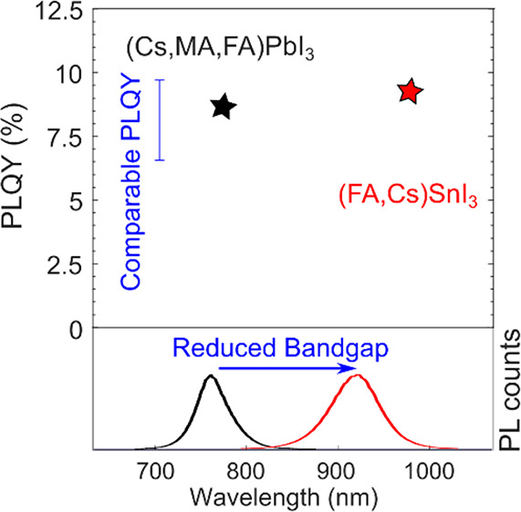
We show that pristine thin films made of tin halide perovskite have external photoluminescence quantum yield comparable to that of lead halide perovskite, i.e., the material in use to prepare state-of-the-art perovskite solar cells.
Tin halide perovskite semiconductors are excellent candidates among the lead-free options for a wide variety of applications in the field of (opto)electronics. In the photovoltaic (PV) sector, particular attention has been paid to ASnI3, where A is a mono-positive cation (typically methylammonium, MA+, formamidinium, FA+, Cs+ or a mixture thereof), both because of reduced toxicity and because such compounds exhibit bandgaps that are better matched to the solar spectrum for maximum power conversion efficiency (PCE) of a single-junction device.1 Despite the great promise, the efficiency of 3D ASnI3 PV devices is still limited with a high voltage loss, which is larger compared to that in the lead-based perovskite solar cell (PSC) counterparts. Currently, good devices with bandgaps of about 1.35 eV generally achieve open-circuit voltage (VOC) and PCE of only 0.6 V and 8%, respectively,2 with champion values of about 0.9 V and 12% (Sn-based thin films with 1.4 eV bandgap).3
The main weakness of these devices has been considered to be the high tendency of Sn(II) to form Sn(IV) in the active material, which translates into high Sn-vacancy densities and strong self-doping. For these reasons, substantial efforts have been put into limiting the oxidation of Sn(II) through the use of additives and reducing agents.4−6 However, a profound understanding of the photophysics and photochemistry of defects in Sn-containing materials is still lacking. This should start from the evaluation of the optoelectronic quality of Sn-containing thin films. The fraction of radiative recombination upon photoexcitation is a good figure of merit, since ideal light-emitting and PV diodes operate at the radiative limit. For PV devices, any non-radiative loss will reduce the carrier concentration, and thus the quasi-Fermi-level splitting and the maximum achievable VOC.
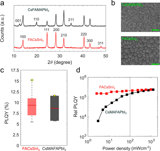
In this study we compare pristine (i.e., not subjected to any passivation process) FA0.85Cs0.15SnI3 (FACsSnI3) and Cs0.05(FA0.85MA0.15)0.95Pb(I0.85Br0.15)3 (CsFAMAPbI3) thin films prepared by spin-coating with antisolvent. Thin films were prepared in a N2-filled glovebox and glass encapsulated immediately after perovskite film annealing under extremely low (sub-ppm) oxygen concentrations. The photoluminescence (PL) and UV–vis absorption spectra can be found in Figure S1. The PL peak positions and absorbance onsets of Sn- and Pb-based thin films give optical bandgaps of about 1.35 and 1.60 eV, respectively. Both films are highly crystalline, as shown by the X-ray diffraction (XRD) patterns in Figure 1a. The top-view scanning electron microscopy (SEM) images shown in Figure 1b demonstrate that both films exhibit full coverage and good morphology—the Sn-containing film presents larger grains of about 500 nm compared to the Pb-containing counterpart, which instead has an average grain size of approximately 100 nm. Figure 1c shows the external photoluminescence quantum yield (PLQY) of seven different Sn- and Pb-containing films measured at ∼100 mW cm–2 with 450 nm excitation (see Figure S2 for details on how to calculate the PLQY). The two materials present similar values of about 9%; similar results are also observed for triple-cation Sn-based perovskite materials (Figure S3). Figure 1d shows the relative PLQYs of FACsSnI3 and CsFAMAPbI3 thin films taken with increasing excitation density. Both films show similar relative PLQYs at excitation density close to 1 sun equivalent excitation. However, the relative PLQY of the Pb-based film increases as a function of the excitation power. In contrast, the Sn-containing film shows a PLQY with a very weak slope, almost flat when the excitation density is increased over 2 orders of magnitude. These are typical trends in the presence of dominant deep and shallow carrier trap states respectively for Pb- and Sn-based perovskite thin films (see section S2.4 of the Supporting Information in ref (7)). Therefore, the carrier recombination dynamics in Sn-based perovskite thin films are dominated by shallow trap states which are likely responsible for the notorious self-doping mechanism. In agreement, the time-resolved PL decay is monomolecular (about 4 ns lifetime) and independent of the excitation density over several orders of magnitude (Figure S4), which is a clear fingerprint of electronic doping. Such observations are in agreement with theoretical predictions by Meggiolaro et al., who showed that enhancement of the valence band when Sn substitutes Pb leads to the suppression of deep transitions associated with under-coordinated iodine defects that are typical of MAPbI3.8
Figure 1.
(a) XRD patterns of Pb-based and Sn-based thin-film perovskites. All the XRD peaks marked in the panel are associated with the 3D tetragonal perovskite phase except 001, which is associated with crystalline PbI2 residual. (b) Top-view SEM images of Pb-based (top panel, scale bar 1 μm) and Sn-based (bottom panel, scale bar 1 μm) thin-film perovskites. (c) External PLQY of FACsSnI3 (red boxes, 5 samples from 4 different batches) and CsFAMAPbI3 (black boxes, 2 samples from 2 different batches) thin films measured using an integrating sphere system at ∼100 mW cm–2. The red lines and stars indicate the average and champion values, respectively. (d) Relative PLQY of FACsSnI3 (PLQY = 12.88% at ∼10 W cm–2, 450 nm) and CsFAMAPbI3 (PLQY = 11.92% at ∼10 W cm–2) films taken with increasing excitation intensities (cw illumination, 450 nm, 6 s excitation time for each data point, and 30 s hold time between data points). The dotted line represents an excitation density close to 1 sun excitation.
For pristine lead-based thin-film perovskite layers, the external PLQY at 1 sun equivalent photon flux is typically <15%.9 In line with this, the measured sample, when embodied in solar cells, leads to devices with a PCE of the order of 18% (a typical current density–voltage curve is shown in Figure S5). The result is surprising when looking at the Sn-based thin film because it indicates that a similar or even higher fraction of photogenerated carrier recombines radiatively when compared to the more successful lead-based counterpart, despite the shorter lifetime. This suggests that the optoelectronic quality of state-of-the-art pristine Sn-based perovskite thin films is inherently good for the fabrication of solar cells with a higher VOC and PCE. Nevertheless, the device performance is not as expected. Thus, re-designing the device architecture can be a promising way to boost the performance.
Acknowledgments
The authors thank Prof. Antonio Abate, Prof. Filippo De Angelis, and Prof. Guglielmo Lanzani for useful discussions. This work has been funded by the European Union project PERT PV under grant agreement no. 763977, ERC project SOPHY under grant agreement no. 771528, and SMART-X under grant agreement no. 860553.
Supporting Information Available
The Supporting Information is available free of charge at https://pubs.acs.org/doi/10.1021/acsenergylett.0c02612.
Figures S1–S5, showing UV–vis and PL spectra, TRPL decays, and JV curves, and experimental details (PDF)
The authors declare no competing financial interest.
Supplementary Material
References
- Nasti G.; Abate A. Tin Halide Perovskite (ASnX3) Solar Cells: A Comprehensive Guide toward the Highest Power Conversion Efficiency. Adv. Energy Mater. 2020, 10, 1902467. 10.1002/aenm.201902467. [DOI] [Google Scholar]
- Zhao Z.; Gu F.; Li Y.; Sun W.; Ye S.; Rao H.; Liu Z.; Bian Z.; Huang C. Mixed-Organic-Cation Tin Iodide for Lead-Free Perovskite Solar Cells with an Efficiency of 8.12%. Adv. Sci. 2017, 4 (11), 1700204. 10.1002/advs.201700204. [DOI] [PMC free article] [PubMed] [Google Scholar]
- Jiang X.; Wang F.; Wang C.; Cheng P.; Chen Q.; Chen L.; et al. Ultra-High Open-Circuit Voltage of Tin Perovskite Solar Cells via an Electron Transporting Layer Design. Nat. Commun. 2020, 11, 1245. 10.1038/s41467-020-15078-2. [DOI] [PMC free article] [PubMed] [Google Scholar]
- Song T. B.; Yokoyama T.; Logsdon J.; Wasielewski M. R.; Aramaki S.; Kanatzidis M. G. Piperazine Suppresses Self-Doping in CsSnI3 Perovskite Solar Cells. ACS Appl. Energy Mater. 2018, 1 (8), 4221–4226. 10.1021/acsaem.8b00866. [DOI] [Google Scholar]
- Yang Z.; Yu Z.; Wei H.; Xiao X.; Ni Z.; Chen B.; Deng Y.; Habisreutinger S. N.; Chen X.; Wang K.; Zhao J.; Rudd P. N.; Berry J. J.; Beard M. C.; Huang J. Enhancing Electron Diffusion Length in Narrow-Bandgap Perovskites for Efficient Monolithic Perovskite Tandem Solar Cells. Nat. Commun. 2019, 10 (1), 1–9. 10.1038/s41467-019-12513-x. [DOI] [PMC free article] [PubMed] [Google Scholar]
- Lin R.; Xiao K.; Qin Z.; Han Q.; Zhang C.; Wei M.; Saidaminov M. I.; Gao Y.; Xu J.; Xiao M.; Li A.; Zhu J.; Sargent E. H.; Tan H. Monolithic All-Perovskite Tandem Solar Cells with 24.8$\%$ Efficiency Exploiting Comproportionation to Suppress Sn(II) Oxidation in Precursor Ink. Nat. Energy 2019, 4, 864–873. 10.1038/s41560-019-0466-3. [DOI] [Google Scholar]
- Srimath Kandada A. R.; Neutzner S.; D’Innocenzo V.; Tassone F.; Gandini M.; Akkerman Q. A.; Prato M.; Manna L.; Petrozza A.; Lanzani G. Nonlinear Carrier Interactions in Lead Halide Perovskites and the Role of Defects. J. Am. Chem. Soc. 2016, 138 (41), 13604–13611. 10.1021/jacs.6b06463. [DOI] [PubMed] [Google Scholar]
- Meggiolaro D.; Ricciarelli D.; Alasmari A. A.; Alasmary F. A. S.; De Angelis F. Tin vs. Lead Redox Chemistry Modulates Charge Trapping and Self Doping in Tin/Lead-Iodide Perovskites. J. Phys. Chem. Lett. 2020, 11, 3546–3556. 10.1021/acs.jpclett.0c00725. [DOI] [PubMed] [Google Scholar]
- Braly I. L.; Dequilettes D. W.; Pazos-Outón L. M.; Burke S.; Ziffer M. E.; Ginger D. S.; Hillhouse H. W. Hybrid Perovskite Films Approaching the Radiative Limit with over 90% Photoluminescence Quantum Efficiency. Nat. Photonics 2018, 12 (6), 355–361. 10.1038/s41566-018-0154-z. [DOI] [Google Scholar]
Associated Data
This section collects any data citations, data availability statements, or supplementary materials included in this article.


