

Abstract

Perovskite-based tandem solar cells are of increasing interest as they approach commercialization. Here we use experimental parameters from optical spectroscopy measurements to calculate the limiting efficiency of perovskite–silicon and all-perovskite two-terminal tandems, employing currently available bandgap materials, as 42.0% and 40.8%, respectively. We show luminescence coupling between subcells (the optical transfer of photons from the high-bandgap to low-bandgap subcell) relaxes current matching when the high-bandgap subcell is a luminescent perovskite. We calculate that luminescence coupling becomes important at charge trapping rates (≤106 s–1) already being achieved in relevant halide perovskites. Luminescence coupling increases flexibility in subcell thicknesses and tolerance to different spectral conditions. For maximal benefit, the high-bandgap subcell should have the higher short-circuit current under average spectral conditions. This can be achieved by reducing the bandgap of the high-bandgap subcell, allowing wider, unstable bandgap compositions to be avoided. Lastly, we visualize luminescence coupling in an all-perovskite tandem through cross-section luminescence imaging.
The performances of halide perovskite solar cells, epitomized by the workhorse methylammonium lead iodide (MAPbI3) composition, have rapidly improved over the past decade, and power conversion efficiencies now rival those of silicon.1 Perovskites are ideal light-harvesting layers for solar cells due to strong absorption coefficients, long charge diffusion lengths, and tolerance to charge traps.2 Importantly, the bandgap of halide perovskites can be controlled via the substitution of a fraction of lead for tin (decreasing the bandgap from ∼1.6 to ∼1.2 eV) or chlorine and bromine for iodine (increasing the bandgap to ∼2.3 and 3 eV, respectively, in pure-lead systems).3,4 This tunability means perovskites hold great promise for realizing cheap and efficient tandem solar cells in which two absorber layers of different bandgaps harvest complementary regions of the solar spectrum. To date, all-perovskite tandems have achieved certified efficiencies of 24.8% and silicon–perovskite tandems efficiencies of 29.1%.1,5 Importantly, both of these tandem technologies are predicted to realize a sufficiently low levelized cost of electricity to make them competitive with market-leading single-bandgap silicon solar cells.6 As tandem perovskite solar cells continue to improve, it is important to understand fully their thermodynamic efficiency limits and any current matching conditions required for optimal operation, both of which impose restrictions on material and device design. While there are several reports estimating all-perovskite and perovskite–silicon tandem efficiency limits and optimal optical designs, a majority focus on what can be achieved with current technologies (e.g., for transmission from top contacts) and, critically, do not include all intrinsic recombination and luminescence coupling processes.7−13 This means that tandem device optimization is currently being guided by incomplete models that do not capture all effects.
Here we measure intrinsic recombination rates and absorption coefficients in perovskite thin films using time-resolved and steady-state optical spectroscopy and use these values to calculate the thermodynamic efficiency limits of low-bandgap perovskite formamidinium lead–tin iodide (FAPb0.5Sn0.5I3) as 32.1%, an all-perovskite tandem, with the same low bandgap system coupled to FA0.7Cs0.3Pb(I0.7Br0.3)3, as 40.8%, and this high-bandgap system coupled to an idealized silicon absorber layer as 42.0% (using literature recombination rates and absorption coefficients for silicon). We demonstrate that consideration of luminescence coupling between subcells, i.e., the emission of light from the high-bandgap subcell and its subsequent reabsorption in the low-bandgap subcell, relaxes the need for current matching compared to previous calculations that do not include the effect. It becomes important when charge trapping rates are <106 s–1 in all-perovskite tandems and <105 s–1 in perovskite–silicon tandems, values comparable to those already being achieved in reported materials, where charge lifetimes in the charge-trapping regime are on the order of 1–10 μs.14,15 Furthermore, via exploration of a range of experimental device optimization parameters, we show consideration of luminescence coupling which allows for greater flexibility in the choice of subcell thicknesses and bandgaps in a tandem cell, alongside increased tolerance to a range of real-world spectral conditions. Using an all-perovskite tandem cell, we provide proof-of-concept spectroscopic visualization and electrical measurements of luminescence coupling, demonstrating the direct implications of our work for further perovskite device optimization.
The maximum efficiency of a single-bandgap solar cell was derived in the seminal paper by Shockley and Queisser16 and extended to include any number of ideal tandem solar cells by de Vos.17 Considerations relevant to specific material systems, for example, non-ideal absorption and intrinsic nonradiative loss mechanisms, were first included for single-junction silicon solar cells and more recently for MAPbI3 solar cells.18,19 Efficiency models are based on calculating the extracted current as the difference between generated charges, Jsc, and those lost to recombination, J0(V):
| 1 |
where V is the voltage across the semiconductor (in an ideal case assumed to be equal to the Fermi-level splitting) and the maximum efficiency is found by maximizing the product (JV)/(incident power).
When considering tandem solar cells, an additional intrinsic process should be included when compared to single-junction devices: luminescence coupling between the subcells. This phenomenon has been previously explored in idealized systems20,21 and III–V tandem technologies22−28 but has not been considered in perovskite technologies. We first briefly discuss luminescence coupling, especially its importance to perovskite tandems, within an idealized Shockley–Queisser formalism, before presenting results using experimental parameters and including other non-ideal absorption and loss processes. We consider that the density of blackbody radiation is higher in a semiconductor than in its surroundings by a factor of n(E)2, the real refractive index at energy E, due to the increased density of states.29 Light emitted from any material can interact with its surroundings [where n(E) ∼ 1] only through its light escape cone, reducing the fraction of blackbody radiation by a factor of 1/[n(E)2] (so semiconductors are still in equilibrium with their surroundings). However, between two tandem subcell absorbers with refractive indices of >1, the escape cone covers a solid angle that is larger than that with the surroundings by a factor of n(E)x2 (where x refers to the lowest index of refraction of the semiconductors). Typically, the high-bandgap subcell can absorb only a small fraction of the light emitted by the low-bandgap subcell, as most emitted light is below its bandgap. However, the low-bandgap cell can absorb a significant fraction of radiation emitted by the high-bandgap cell (see the schematic in the inset of Figure 1b). In a two-terminal tandem solar cell, the same current must flow through both subcells. Therefore, at a maximum power point, the maximum number of extracted charges is determined by the subcell with the minimum number of photogenerated charges. If the low-bandgap subcell is the limiting subcell, charges not extracted from the high-bandgap subcell can recombine radiatively and be reabsorbed in the low-bandgap subcell, reducing the current mismatch.
Figure 1.

Limiting efficiency of an ideal Shockley–Queisser-like tandem (where all light above the bandgap is absorbed) (a) without and (b) with luminescence coupling. Crosses mark bandgap pairs yielding the highest efficiency. The inset schematics demonstrate the system being modeled, with LG and HG corresponding to the low- and high-bandgap subcells, respectively, blue and yellow arrows denoting absorbed incident solar radiation in the HG and LG cells, respectively, and other arrows corresponding to re-emitted light. (c) Ratio of these two graphs, with the dashed line marking the case in which there is no change when including luminescence coupling. (d) Line slices of panels a and b (as marked by dotted vertical lines on the respective panels) showing the efficiency of tandem cells, without and with luminescence coupling, when the bandgap of the low-energy absorber is set to 1.25 eV.
In Figure 1, we present the limiting efficiency of Shockley–Queisser-like tandem solar cells under AM1.5 (where all light above the bandgap is absorbed and the only loss process is radiative recombination) without considering luminescence coupling between the subcells (Figure 1a), as has been presented in the perovskite field to date, and compare this to the case that includes luminescence coupling (Figure 1b). The ratio of these efficiencies is shown in Figure 1c. We note it is possible to prevent luminescence coupling in this fully idealized case by use of a suitable dichroic mirror between the subcells (reflecting all light emitted from the back of the high-bandgap subcell), while in real systems, it cannot be prevented due to absorption coefficients not being step functions (i.e., there will be a spectral region where both high- and low-bandgap subcells absorb light and can therefore couple). Here we have used an n(E)x value of 2.5, representative of metal halide perovskites (cf. Figure 2c,d). Luminescence coupling between layers lowers the maximum possible efficiency from 45.8% to 44.9% due to more light being lost from the high-bandgap subcell than in the case without coupling. While the optimal bandgap pair remains within 0.01 eV of that without luminescence coupling (0.94 and 1.60 eV for the low- and high-bandgap subcells, respectively), Figure 1b demonstrates that luminescence coupling gives greater tolerance in the choice of subcell bandgaps to achieve a high efficiency. Specifically, when the short-circuit current of the high-bandgap subcell is significantly larger than that of the low-bandgap subcell, the efficiency is increased when luminescence coupling is included. This beneficial region can be seen below the diagonal dashed line of Figure 1c (see Figure S1 for a plot of the short-circuit current in each subcell and a ratio of the two). To further illustrate how this result impacts device design for the case of halide perovskites, we plot line slices of panels a and b of Figure 1 in Figure 1d with the low bandgap fixed at 1.25 eV, close to the lowest bandgap currently technically feasible for halide perovskites,30 and we vary the high bandgap. Our results demonstrate that the high bandgap can be reduced to ∼1.6–1.7 eV with a minimal loss of efficiency, compared to the much less stable bandgaps in the range of 1.8–1.9 eV (which typically require large fractions of bromide and/or cesium) required in the case without luminescence coupling,7 by relaxing current matching requirements.
Figure 2.

(a) Plot of dn/dt vs carrier density n (time is an implicit variable) extracted from transient absorption decay measurements of FA0.7Cs0.3Pb(I0.7Br0.3)3 thin films. Each symbol represents a different decay measurement, corresponding to a different initial excitation density. The red line is a fit to the data using eq 2. (b) Plot of generation rate × PLQE (black symbols) vs carrier density n (extracted from the TA measurements) for FA0.7Cs0.3Pb(I0.7Br0.3)3 thin films. The red line is a fit to the data using eq 3. Absorption coefficients and refractive indices of (c) FA0.7Cs0.3Pb(I0.7Br0.3)3 and (d) FAPb0.5Sn0.5I3 as measured by a combination of ellipsometry and photothermal deflection spectroscopy (see Figure S3 and SI Note 2 for details). Parameters extracted from these fits and optical analysis are summarized in Table 1, SI Table 1, and SI Table 2.
We now focus on the state-of-the-art experimental FAPb0.5Sn0.5I3 and FA0.7Cs0.3Pb(I0.7Br0.3)3 tandem compositions as low-bandgap (1.25 eV) and high-bandgap (1.7 eV) subcells, respectively,14,31 which we solution process as thin films (see Methods in the Supporting Information). We use a combination of transient absorption spectroscopy (TA) and photoluminescence quantum efficiency (PLQE) to quantify decay rates in each material. In halide perovskites, charges have been observed to decay according to first-, second-, and third-order mechanisms,32,33 typically interpreted as nonradiative recombination via traps (with rate a), bimolecular recombination (with rate b, a component of which is radiative32), and nonradiative Auger recombination (rate c), respectively. These processes are described by
| 2 |
where n is the excited charge density and t is time. In both materials, we observe a broad ground-state bleach in TA that scales linearly with excitation density (see Figure S2), and we integrate about the peak of this bleach. We estimate the excitation density, n, using the same approach as Richter et al.,32 and by scaling the bleach appropriately, we present dn/dt versus n in Figure 2a for the FA0.7Cs0.3Pb(I0.7Br0.3)3 thin film (see Methods in the Supporting Information). We fit this decay with the first-, second-, and third-order decay rates described in eq 2 (red line). For our PLQE measurements, we consider
| 3 |
where Gext is the laser generation rate, ηesc is the photon escape probability, br is the internal radiative bimolecular recombination rate, and pi is the background hole concentration (in the case of a p-type material). By measuring the laser generation rate, Gext, and calculating n from values obtained in our TA measurements (as Gext = an + bn2 + cn3), we fit our PLQE data using eq 3 to extract the background hole concentration and ηescbr (Figure 2b). We note that we do not observe any phase segregation during these measurements (Figure S2). For the low-bandgap system, we use our previously reported doping densities, radiative bimolecular rates, and Auger recombination rates (Table 1).31
Table 1. Relevant Parameters Extracted from the Time-Resolved and Steady-State Optical Characterization of FAPb0.5Sn0.5I3 and FA0.7Cs0.3Pb(I0.7Br0.3)3 Thin Filmsa.
| FAPb0.5Sn0.5I3 | FA0.7Cs0.3Pb(I0.7Br0.3)3 | |
|---|---|---|
| internal bimolecular recombination rate, br (cm3 s–1) | (3.0 ± 0.2) × 10–12 | (5.1 ± 0.2) × 10–10 |
| Auger recombination rate, c (cm6 s–1) | (6.5 ± 2.0) × 10–29 | (7.5 ± 2.0) × 10–29 |
| nipi (cm–6) | (2.7 ± 0.2) × 1017 | (1.2 ± 0.1) × 108 |
| Urbach energy (meV) | 16.1 ± 0.1 | 14.4 ± 0.1 |
See SI Table 1 for all extracted parameters from our measurements.
To measure optical constants for
both materials, we combined ellipsometry
and photothermal-deflection spectroscopy (PDS) measurements19 (Figure S3). For
the purposes of our calculations, we fit the below-bandgap region
with an Urbach tail using photoluminescence (PL) spectra to quantify
only absorption that clearly contributes to PL (Figure S4). The combination of these measurements and the
Urbach fit gives us absorption coefficients, α(E), and refractive indices, n(E),
for all relevant energies, which we plot in panels c and d of Figure 2 for the high- and
low-bandgap systems, respectively. Using these optical constants,
we simulate the internal PL spectra of our materials and compare these
with the recorded (external) PL spectra to determine the escape probability, ηesc, for each sample without the need
for any assumptions about the absorption of the material (see Figure S5 and SI Note 2 for further details). The value of ηesc allows us to calculate the intrinsic radiative rate, br. We estimate the background minority carrier
concentration, ni, following the approach
of Pazos-Outón et al.19 and use
our measurements to calculate the equivalent intrinsic doping density,  . We
note that although the low- and high-bandgap
perovskites we measured are observed to be doped systems, we herein
model the absorber layers as intrinsic layers because such background
doping densities do not significantly affect limiting efficiencies
(see Figure S6 and SI Note 3). We summarize all relevant experimentally extracted
parameters for calculations in Table 1 and others in SI Table 1.
. We
note that although the low- and high-bandgap
perovskites we measured are observed to be doped systems, we herein
model the absorber layers as intrinsic layers because such background
doping densities do not significantly affect limiting efficiencies
(see Figure S6 and SI Note 3). We summarize all relevant experimentally extracted
parameters for calculations in Table 1 and others in SI Table 1.
A key ingredient in a limiting efficiency calculation is the fraction of sunlight absorbed at each energy E, a(E), as calculated from the measured absorption coefficients and refractive indices (Figure 2). Yablonovitch demonstrated that it is possible to increase the absorption of a semiconductor significantly beyond an exponential Beer–Lambert-type law close to its bandgap by considering rough front and back surfaces that randomize the direction of light inside a semiconductor, and a perfect back reflector.34 This model, which we term Randomized, has previously been used as the workhorse for calculating the absorption of idealized single-bandgap perovskite solar cells.19,35 However, in a tandem stack the Randomized model predicts weak absorption above the bandgap in the low-bandgap subcell when compared to Beer–Lambert absorption, as is shown in Figure 3a [for a tandem stack of FAPb0.5Sn0.5I3 and FA0.7Cs0.3Pb(I0.7Br0.3)3 assuming no parasitic absorption and subcell thicknesses of 1000 and 440 nm, respectively (see Figure S7 for high-bandgap results)]. This is due to light being treated as blackbody radiation once it has entered the high-bandgap material, meaning some of it never reaches the low-bandgap subcell, but is instead directly re-emitted to the surroundings. To resolve this problem, we use a more advanced Lambertian absorption model that combines Randomized and Beer–Lambert-type absorptances, termed Hybrid. This is an extension of Green’s Lambertian absorptance model to idealized tandem solar cells36 (see SI Notes 4 and 5 for full details). We apply this absorption model to single-bandgap perovskite solar cells in SI Note 5 and demonstrate the limiting efficiency of low-bandgap FAPb0.5Sn0.5I3 perovskite as 32.1% (Figure S8). We note that photon recycling within a single perovskite layer is implicitly included within all absorption models.
Figure 3.

(a) Absorptance in the low-bandgap FAPb0.5Sn0.5I3 absorber of the tandem solar cell stack, for the three absorptance models described in the main text, for low- and high-bandgap subcell thicknesses of 1000 and 440 nm, respectively. We present the limiting efficiency of an all-perovskite [FAPb0.5Sn0.5I3 and FA0.7Cs0.3Pb(I0.7Br0.3)3] tandem as a function of subcell thickness (b) without including and (c) including luminescence coupling in models, ascertained by using experimentally measured parameters but setting charge trapping to zero in both cases. The dashed lines denote regions within 1% of maximum efficiency. (d) Difference in energy generated with and without luminescence coupling throughout the year for North Roseau on the United States–Canada border. Subcell thicknesses are chosen to maximize energy yield in these simulations of 1000 and 220 nm without luminescence coupling and 1000 and 310 nm with luminescence coupling for low- and high-bandgap subcells, respectively (see Figure S12).
To calculate the fundamental limiting efficiency of a solar
cell
at a maximum power point, the absorption is maximized (using the Hybrid
model, which gives less absorption than in Shockley–Queisser
tandems) and the recombination rate is minimized by setting all controllable
loss mechanisms to zero. Therefore, only radiative recombination and
intrinsic nonradiative Auger recombination are included in our limiting
efficiency calculations, while the effects of charge trapping are
considered below. We also assume an equal Fermi-level splitting such
that the populations of electrons (n) and holes (p) as a function of applied voltage V follow
the equation 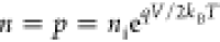 in our intrinsic
approximation, where q is the charge of an electron
and kBT the thermal energy.
in our intrinsic
approximation, where q is the charge of an electron
and kBT the thermal energy.
The limiting efficiency of an all-perovskite tandem under AM1.5 as a function of subcell thickness with experimentally parametrized absorption and recombination coefficients, in the case in which luminescence coupling is not considered in the modeling, is presented in Figure 3b (see SI Note 6 for full calculation details). We emphasize that removing luminescence coupling is not possible in a real device, but this hypothetical case has been assumed in the literature to date and instructive for subsequently demonstrating the importance of this effect. We carry out simulations to 1000 nm as diffusion limitations (which are not included in this model) are likely to become critical at larger thicknesses.19 The maximum efficiency that can be achieved is 41.1% for optimal subcell thicknesses of 1000 nm (low-gap) and 240 nm (high-gap). To be within 1% of the maximum efficiency, the low- and high-bandgap thicknesses need to be in the ranges of 570–1000 nm and 220–270 nm, respectively (dashed line in the figure). This is a narrow range of thicknesses for the subcells due to the requirement for nearly perfect short-circuit current matching and imposes significant restrictions on device material tunability. In Figure 3c, we present the limiting efficiency of the same system but now including the physically intrinsic process of luminescence coupling in our modeling (see details about modeling luminescence coupling between subcells in SI Note 7 and Figure S9). As in Figure 1, the maximum efficiency is slightly decreased in the presence of luminescence coupling (40.8% for low- and high-bandgap subcell thicknesses of 1000 and 440 nm, respectively). For comparison, we note that the limiting efficiency of a Shockley–Queisser tandem (where all light is absorbed above the bandgap) with luminescence coupling is 44.9% (cf. Figure 1b). In the system modeled here, to be within 1% of the maximum efficiency the thickness ranges are now 480–1000 and 260–1000 nm for the low- and high-bandgap subcells, respectively (dashed line on Figure 3c). This demonstrates a substantial increase in thickness tolerance due to any discrepancy in current matching being partly self-corrected through luminescence coupling, as has been discussed in idealized systems.22 We note the combined thickness of both absorber layers can also be decreased by ∼10% when luminescence coupling is included, giving an additional advantage for lightweight applications. We present limiting efficiencies based on the Beer–Lambert model in Figure S10, where a limiting efficiency of 39.7% is found when luminescence coupling is not considered and 39.4% when luminescence coupling is included.
We also model a perovskite–silicon tandem by coupling the same high-bandgap perovskite to an idealized silicon subcell (see SI Note 3 for details and Figure S11 for results). This perovskite has a bandgap better matched to that of silicon than of the low-bandgap perovskite considered above (cf. Figure 1a), giving a limiting efficiency of 43.0% without luminescence coupling being included in calculations (for subcell thicknesses of 580 μm and 1000 nm in the silicon and perovskite subcells, respectively). The efficiency limit is reduced to 42.0% when the more physically realistic model, including luminescence coupling, is used for respective subcell thicknesses of 270 μm and 1000 nm. Luminescence coupling is again seen to increase the subcell thickness tolerance, in particular allowing for thinner low-bandgap (silicon) subcells, with the most commercially relevant silicon thicknesses of ∼180 μm within 1% of the maximum calculated efficiency. Furthermore, even thinner silicon subcells still give efficiencies close to the maximum (e.g., 50 μm is within 2% of the maximum efficiency), which could allow for a range of ultrathin silicon fabrication techniques with possible cost benefits.37
To explore how luminescence coupling affects tolerance to real-world spectra, we again consider the all-perovskite tandem cells constructed from our experimental films and calculate the energy generated from a year’s worth of irradiance spectra without and with luminescence coupling. We used a typical meteorological years’ worth of data from the National Solar Radiation Database, which includes spectrally resolved data and temperature variation, for a region on the border between the United States and Canada (North Roseau) that represents reasonable spectral variation throughout the year.13,38 We also note that the Lambertian absorption model treats incident light from all angles equally, allowing for a simplification in the calculations. We first calculate the total energy generated for a range of different subcell thicknesses, as presented in panels a and b of Figure S12. The optimal thickness of the high-bandgap subcell is decreased compared to that of AM1.5 (240 to 220 nm without coupling, 440 to 310 nm with coupling), due to North Roseau having fewer clear days and thus less blue light than AM1.5. More importantly, while perovskite tandems that include the intrinsic process of luminescence coupling in modeling gave a lower efficiency under AM1.5, a comparable total energy yield is generated over the course of a year (492.4 kWh m–2 with luminescence coupling, compared to 492.1 kWh m–2 without). This energy is also generated at different times of the year, as shown in Figure 3d, which shows the difference in energy generation with and without luminescence coupling each day for optimal thicknesses. When luminescence coupling is included in models, more energy is generated in the winter months while slightly less is generated midsummer. We explain this by noting that the days in winter have a less blue spectrum (Figure S12c). If a solar cell is optimized for these less blue conditions, then in midsummer (a bluer spectrum) luminescence coupling can transfer current from the high- to low-bandgap subcell, correcting for the mismatch in current. We confirm this by calculating the percentage of current from a low-bandgap subcell that is generated from luminescence coupling, which is closer to zero in winter but increases to ≤10% in midsummer (Figure S12d). These results demonstrate the increased spectral tolerance imparted on an all-perovskite tandem cell design when considering luminescence coupling under real-world conditions, in agreement with previous analyses of idealized systems by Brown and Green.21
In Figure 4a, we present the limiting efficiency of an experimentally parametrized all-perovskite tandem cell, including the intrinsic process of luminescence coupling in calculations, as a function of nonradiative charge trapping rate a for optimized thicknesses of 1000 and 440 nm. We observe that increasing the charge trapping rate in either material has a similar effect in terms of decreasing the efficiency of the tandem. Figure 4b presents the ratio of Figure 4a to an equivalent calculation neglecting luminescence coupling in models (Figure S13). It is clear that luminescence coupling plays a significant role only when charge trapping rates a < 106 s–1 in the high-bandgap subcell, equivalent to charge lifetimes being longer than 1 μs in the charge trapping regime. Furthermore, we confirm that even with non-zero charge trapping rates, current matching conditions are relaxed when luminescence coupling is included in simulations compared to the case that does not include luminescence coupling (Figure S14). This critical charge trapping rate in the high-bandgap cell for luminescence coupling to be important in perovskite-silicon cells is ∼105 s–1 (Figure S11). We attribute this lower charge trapping rate in the perovskite–silicon tandems to the subcells having better bandgap matching, meaning that the low-bandgap subcell is not current-limiting, and thus, charge densities (and hence the likelihood of radiative recombination) are lower in the high-bandgap subcell. Other simulations confirm the trapping rate for luminescence coupling varies between 105 and 106 s–1 depending on how well current-matched the subcells are (see Figure S15). In both tandem technologies, our results show that luminescence coupling becomes important when the high-bandgap subcell has an external photoluminescence quantum efficiency (PLQE) of at least ∼0.1% at a maximum power point (see Figures S11, S13, and S15 for PLQE calculations for each case and SI Note 6). We mark trapping rates from current state-of-the-art films in the literature with a cross on panels a and b of Figure 4 to demonstrate that we are already realizing conditions in which luminescence coupling becomes important, and thus, we expect that these effects must be considered in the further development of all tandem cells.14,31,39 To maximize the luminescence coupling in a real tandem cell, any interlayer between the subcells should have a (real) refractive index at least as high as that of the perovskite subcells, so the escape cone from the high to low subcell remains as large as possible. We also emphasize that luminescence coupling is an intrinsic process that cannot be prevented from occurring (see SI Note 8).
Figure 4.

Limiting efficiency of all-perovskite tandem solar cells comprised of the experimental FAPb0.5Sn0.5I3 and FA0.7Cs0.3Pb(I0.7Br0.3)3 absorbers with optimized thicknesses of 1000 and 440 nm as a function of charge trapping rate with (a) luminescence coupling and (b) the ratio of this model to the efficiency without including luminescence coupling for the same film thicknesses. Marked crosses correspond to charge trapping rates in current state-of-the-art films.14,31,39
To experimentally demonstrate luminescence coupling and its effect on actual tandem devices, we perform measurements on an all-perovskite tandem cell following the device architecture of Palmstrom et al.40 We first consider a case in which the short-circuit current of the high-bandgap subcell is significantly higher than that of the low-bandgap subcell through selective illumination of the top cell with 405 nm excitation (absorption depth of <50 nm). We observe current from the device at different applied voltages (Figure S16) and, importantly, luminescence from the high-bandgap subcell at all applied voltages (Figure 5a); even when the tandem stack is at short circuit, the high-bandgap luminescence is still 4% of the intensity as at open circuit. Furthermore, we determine the quasi-Fermi-level splitting (QFLS) of the high- and low-bandgap subcells by analyzing the PL properties of each absorber layer in a device stack (see Methods in the Supporting Information and Figure S17 for fits), which corresponds to the maximum open-circuit voltage (VOC) that each subcell can contribute to the tandem stack. Under 405 nm excitation, we observe that the VOC of the tandem exceeds the QFLS of the high-bandgap subcell, meaning that the low-bandgap subcell must be contributing notable voltage, despite the high bandgap absorbing nearly all photons (Figure S18).
Figure 5.

(a) Photoluminescence (PL) of the high-bandgap (HG) subcell in the tandem stack, relative to that when the tandem is held at open circuit (O.C.), as a function of voltage when the HG subcell is selectively excited with 405 nm excitation from the top side, as shown in the schematic (LG corresponds to the low-bandgap subcell). The inset shows the HG PL when the tandem stack is held at O.C. and short-circuit (S.C.). (b) PL maps of the tandem cross section when exciting with a 636 nm laser and using a 775 nm short pass or long pass filter to observe only PL from the high- or low-bandgap subcells, respectively. (c) Fixed excitation at the center of the HG subcell with 636 nm excitation and spatially varying the PL detection away from the excitation spot across the device cross section, using 750 nm short pass and 800 nm long pass filters to collect emission from HG and LG materials, respectively. Note the distance scale here does not exactly correspond to distances on the sample surface (see SI Note 9). (d) Time-resolved PL of the HG and LG regions, as well as the square root of the low-bandgap decay to show the match with the HG decay.
A confocal PL map of a cross section of the tandem using appropriate optical filters to selectively observe emission from the high- or low-bandgap subcell is shown in Figure 5b. We then excited the center of the high-bandgap subcell with a pulsed excitation and, while keeping the excitation spot fixed, spatially scanned the selective PL detection across the cross section (Figure 5c), revealing emission from the low-bandgap cell after excitation in the high-gap cell. To confirm this is luminescence coupling, we consider that the number of photons absorbed in the low gap at time t is proportional to the time-resolved photoluminescence (TRPL) from the high gap, PLHG(t). At low excitation densities, the low-gap TRPL is extremely short (Figure S19). Therefore, if the TRPL signal from the low-gap absorber at time t is due to recombination of excited electrons and holes, the quantity should be proportional to PLHG(t)2; this is exactly what we observe in Figure 5d (see SI Note 9 for further discussion and additional cross section results). These collective results demonstrate that the high-bandgap subcell is luminescent within an operating tandem stack and that these emitted photons can be absorbed in the low-bandgap subcell (i.e., luminescence coupling).
In this work, we have calculated the limiting efficiencies of perovskite-based tandem solar cells, including all intrinsic loss processes and luminescence coupling between subcells. By measuring the recombination rates and absorption coefficients of low- and high-bandgap perovskite films, we calculated the limiting efficiency of an all-perovskite tandem as 40.8% and that of a perovskite–silicon tandem as 42.0% when the intrinsic process of luminescence coupling between the subcells is included and in the absence of trapping. We show that current state-of-the-art high-bandgap perovskite films for tandem cells have charge trapping rates and luminescence quantum efficiencies on the order required for luminescence coupling to play an important role in devices, which reduces the need for short-circuit current matching compared to earlier predictions that do not consider luminescence coupling. We demonstrate luminescence coupling in perovskite tandems, when compared to a model that ignores this effect, gives increased tolerance in the choice of bandgaps, subcell thicknesses, and greater tolerance to a range of real-world spectra and hence relaxes the previously determined criteria for materials and device design. We conclude with a new design rule for perovskite tandems: it is always better for the high-bandgap material to have the higher short-circuit current, as any discrepancy in current matching will be partially corrected by luminescence coupling between subcells. Importantly, these guidelines allow unstable >1.7 eV high-bandgap perovskite absorbers to be avoided when targeting maximum performance. We also present experimental evidence of luminescence coupling occurring in an all-perovskite tandem, including visualization of the effect, highlighting the importance of the effect in ongoing perovskite tandem developments.
Acknowledgments
A.R.B. acknowledges funding from a Winton Studentship, an Oppenheimer Studentship and from the Engineering and Physical Sciences Research Council (EPSRC) Doctoral Training Centre in Photovoltaics (CDT-PV). A.R.B. thanks Luis Pazos-Outón for supplying data for MAPbI3 solar cells. F.L. acknowledges financial support from the Alexander von Humboldt Foundation via the Feodor Lynen program and thanks Prof. Sir R. Friend for supporting his fellowship at the Cavendish Laboratory. Y.-H.C. acknowledges the funding from a Taiwan Cambridge Scholarship. A.J.-S. gratefully acknowledges a postdoctoral scholarship from the Max Planck Society. K.F. acknowledges a George and Lilian Schiff Studentship, a Winton Studentship, an Engineering and Physical Sciences Research Council (EPSRC) studentship, a Cambridge Trust Scholarship, and a Robert Gardiner Scholarship. G.E.E. was funded by the NREL’s LDRD program. E.R. acknowledges the European Research Council (ERC) under the European Union’s Horizon 2020 research and innovation programme (HYPERION, Grant Agreement 756962) and the EPSRC for a DTP Part Studentship. M.A.-J. acknowledges funding support from EPSRC through Program Grant EP/M005143/1. M.A.-J. thanks Cambridge Materials Ltd. for their funding and technical support. M.A. acknowledges funding from the European Research Council (ERC) [Grant Agreement 756962 (HYPERION)] and the Marie Skłodowska-Curie actions (Grant Agreement 841386) under the European Union’s Horizon 2020 research and innovation program. B.V.L. acknowledges funding from the Max Planck Society, the Cluster of Excellence e-conversion and the Center for Nanoscience (CeNS). S.D.S. acknowledges the Royal Society and Tata Group (UF150033) and the EPSRC (EP/R023980/1, EP/T02030X/1, and EP/S030638/1). The authors thank Axel Palmstrom and William Nemeth at NREL for depositing some of the layers in the tandem stack. Data from the manuscript is available at: https://doi.org/10.17863/CAM.63326. Codes are available upon request.
Supporting Information Available
The Supporting Information is available free of charge at https://pubs.acs.org/doi/10.1021/acsenergylett.0c02481.
Methods, terminology definitions, notes about measuring samples, extracting values, full efficiency calculations, absorptances in tandem and single-junction architectures, tandem cell simulation details, models for luminescence coupling, using blocking layers to reduce luminescence coupling, additional discussions of tandem results, parameters obtained from ellipsometry measurements, additional data on short-circuit currents, photoluminescence spectra, ellipsometry data, Urbach energy extractions, use of photoluminescence to estimate escape probability, efficiency results for measured doping levels in all absorber films, absorption in two-terminal tandems for different absorption models, results of low-bandgap single-junction efficiency calculations, absorptance values for luminescence coupling between cells relative to the coupling to the surroundings, limiting efficiency calculations for the Beer–Lambert model, limiting efficiency calculations for perovskite–silicon tandem cells, energy generated using real-world data for an idealized all-perovskite tandem, additional data from all-perovskite tandem calculations, luminescence coupling electrical and optical measurements from real all-perovskite tandems, and X-ray diffraction data (PDF)
Author Present Address
@ Institute for Materials Discovery, University College London, Torrington Place, London WC1E 7JE, United Kingdom.
The authors declare the following competing financial interest(s): S.D.S. and G.E.E. are co-founders of Swift Solar Inc.
Supplementary Material
References
- NREL . Best Research Cell Efficiencies. 2020. https://www.nrel.gov/pv/assets/pdfs/best-research-cell-efficiencies.20200203.pdf (accessed 2020-04-01).
- Green M. A.; Ho-Baillie A.; Snaith H. J. The emergence of perovskite solar cells. Nat. Photonics 2014, 8 (7), 506–514. 10.1038/nphoton.2014.134. [DOI] [Google Scholar]
- Prasanna R.; et al. Band Gap Tuning via Lattice Contraction and Octahedral Tilting in Perovskite Materials for Photovoltaics. J. Am. Chem. Soc. 2017, 139 (32), 11117–11124. 10.1021/jacs.7b04981. [DOI] [PubMed] [Google Scholar]
- Noh J. H.; Im S. H.; Heo J. H.; Mandal T. N.; Seok S. Il Chemical management for colorful, efficient, and stable inorganic-organic hybrid nanostructured solar cells. Nano Lett. 2013, 13 (4), 1764–1769. 10.1021/nl400349b. [DOI] [PubMed] [Google Scholar]
- Lin R.; et al. Monolithic all-perovskite tandem solar cells with 24.8% efficiency exploiting comproportionation to suppress Sn(ii) oxidation in precursor ink. Nat. Energy 2019, 4 (10), 864–873. 10.1038/s41560-019-0466-3. [DOI] [Google Scholar]
- Li Z.; et al. Cost Analysis of Perovskite Tandem Photovoltaics. Joule 2018, 2 (8), 1559–1572. 10.1016/j.joule.2018.05.001. [DOI] [Google Scholar]
- Hörantner M. T.; et al. The Potential of Multijunction Perovskite Solar Cells. ACS Energy Lett. 2017, 2 (10), 2506–2513. 10.1021/acsenergylett.7b00647. [DOI] [Google Scholar]
- Leijtens T.; Bush K. A.; Prasanna R.; McGehee M. D. and M. D. McGehee, “Opportunities and challenges for tandem solar cells using metal halide perovskite semiconductors. Nat. Energy 2018, 3 (10), 828–838. 10.1038/s41560-018-0190-4. [DOI] [Google Scholar]
- Eperon G. E.; Hörantner M. T.; Snaith H. J. Metal halide perovskite tandem and multiple-junction photovoltaics. Nat. Rev. Chem. 2017, 1 (0095), 12. 10.1038/s41570-017-0095. [DOI] [Google Scholar]
- Anaya M.; et al. Optical analysis of CH3NH3Sn:XPb1- xI3 absorbers: A roadmap for perovskite-on-perovskite tandem solar cells. J. Mater. Chem. A 2016, 4 (29), 11214–11221. 10.1039/C6TA04840D. [DOI] [PMC free article] [PubMed] [Google Scholar]
- Anaya M.; Lozano G.; Calvo M. E.; Míguez H. ABX3 Perovskites for Tandem Solar Cells. Joule 2017, 1 (4), 769–793. 10.1016/j.joule.2017.09.017. [DOI] [Google Scholar]
- Futscher M.; Ehrler B. Efficiency Limit of Perovskite/Si Tandem Solar Cells. ACS 2016, 1, 863–868. 10.1021/acsenergylett.6b00405. [DOI] [Google Scholar]
- Hörantner M. T.; Snaith H. Predicting and Optimising the Energy Yield of Perovskite-on-Silicon Tandem Solar Cells under Real World Conditions. Energy Environ. Sci. 2017, 10, 1983–1993. 10.1039/C7EE01232B. [DOI] [Google Scholar]
- Chen C.; et al. Achieving a high open-circuit voltage in inverted wide-bandgap perovskite solar cells with a graded perovskite homojunction. Nano Energy 2019, 61 (March), 141–147. 10.1016/j.nanoen.2019.04.069. [DOI] [Google Scholar]
- Jariwala S.; et al. Approaching the limits of optoelectronic performance in mixed cation mixed halide perovskites by controlling surface recombination. arXiv 2020, 2006.04025v1. [Google Scholar]
- Shockley W.; Queisser H. J. Detailed balance limit of efficiency of p–n junction solar cells. J. Appl. Phys. 1961, 32 (3), 510–519. 10.1063/1.1736034. [DOI] [Google Scholar]
- De Vos A. Detailed balance limit of the efficiency of tandem solar cells. J. Phys. D: Appl. Phys. 1980, 13 (5), 839–846. 10.1088/0022-3727/13/5/018. [DOI] [Google Scholar]
- Tiedje T.; Yablonovitch E.; Cody G. D.; Brooks B. G. Limiting efficiency of silicon solar cells. IEEE Trans. Electron Devices 1984, 31 (5), 711–716. 10.1109/T-ED.1984.21594. [DOI] [Google Scholar]
- Pazos-Outón L. M.; Xiao T. P.; Yablonovitch E. Fundamental Efficiency Limit of Lead Iodide Perovskite Solar Cells. J. Phys. Chem. Lett. 2018, 9, 1703–1711. 10.1021/acs.jpclett.7b03054. [DOI] [PubMed] [Google Scholar]
- Martí A.; Araújo G. L. Limiting efficiencies for photovoltaic energy conversion in multigap systems. Sol. Energy Mater. Sol. Cells 1996, 43, 203–222. 10.1016/0927-0248(96)00015-3. [DOI] [Google Scholar]
- Brown A. S.; Green M. A. Radiative coupling as a means to reduce spectral mismatch in monolithic tandem solar cell stacks-theoretical considerations. Conf. Rec. IEEE Photovolt. Spec. Conf. 2002, 868–871. 10.1109/PVSC.2002.1190717. [DOI] [Google Scholar]
- Strandberg R. Comparison of the sensitivity to spectral variation of voltage- and current-matched tandem devices with luminescent coupling and thickness optimization. 2016 IEEE 43rd Photovoltaic Specialists Conference (PVSC) 2016, 0358–0363. 10.1109/PVSC.2016.7749611. [DOI] [Google Scholar]
- Geisz J. F.; et al. Generalized Optoelectronic Model of Series-Connected Multijunction Solar Cells. IEEE J. Photovoltaics 2015, 5 (6), 1827–1839. 10.1109/JPHOTOV.2015.2478072. [DOI] [Google Scholar]
- Lan D.; Geisz J. F.; Steiner M. A.; Garcia I.; Friedman D. J.; Green M. A. Improved modeling of photoluminescent and electroluminescent coupling in multijunction solar cells. Sol. Energy Mater. Sol. Cells 2015, 143, 48–51. 10.1016/j.solmat.2015.06.036. [DOI] [Google Scholar]
- Pusch A.; Pearce P.; Ekins-Daukes N. J. Analytical Expressions for the Efficiency Limits of Radiatively Coupled Tandem Solar Cells. IEEE J. Photovoltaics 2019, 9 (3), 679–687. 10.1109/JPHOTOV.2019.2903180. [DOI] [Google Scholar]
- Ren Z.; et al. Numerical Analysis of Radiative Recombination and Reabsorption in GaAs/Si Tandem. IEEE J. Photovoltaics 2015, 5 (4), 1079–1086. 10.1109/JPHOTOV.2015.2427580. [DOI] [Google Scholar]
- Steiner M. A.; et al. Optically enhanced photon recycling in mechanically stacked multijunction solar cells. IEEE J. Photovoltaics 2016, 6 (1), 358–365. 10.1109/JPHOTOV.2015.2494690. [DOI] [Google Scholar]
- Essig S.; et al. Realization of GaInP/Si Dual-Junction Solar Cells with 29.8% 1-sun efficiency. IEEE Journal of Photovoltaics 2016, 6 (4), 1012–1019. 10.1109/JPHOTOV.2016.2549746. [DOI] [Google Scholar]
- Nelson J.The Physics of Solar Cells; Imperial College Press: London, 2003. [Google Scholar]
- Werner J.; et al. Improving Low Bandgap Tin Lead Perovskite Solar Cells via Contact Engineering and Gas Quench Processing. ACS Energy Lett. 2020, 5, 1215–1223. 10.1021/acsenergylett.0c00255. [DOI] [Google Scholar]
- Bowman A. R.; et al. Microsecond Carrier Lifetimes, Controlled p-Doping, and Enhanced Air Stability in Low-Bandgap Metal Halide Perovskites. ACS Energy Lett. 2019, 4, 2301–2307. 10.1021/acsenergylett.9b01446. [DOI] [PMC free article] [PubMed] [Google Scholar]
- Richter J. M.; et al. Enhancing photoluminescence yields in lead halide perovskites by photon recycling and light out-coupling. Nat. Commun. 2016, 7, 13941. 10.1038/ncomms13941. [DOI] [PMC free article] [PubMed] [Google Scholar]
- Dequilettes D. W.; et al. Charge-Carrier Recombination in Halide Perovskites. Chem. Rev. 2019, 119 (20), 11007–11019. 10.1021/acs.chemrev.9b00169. [DOI] [PubMed] [Google Scholar]
- Yablonovitch E. Statistical Ray Optics. J. Opt. Soc. Am. 1982, 72 (7), 899–907. 10.1364/JOSA.72.000899. [DOI] [Google Scholar]
- Brenes R.; Laitz M.; Jean J.; DeQuilettes D. W.; Bulović V. Benefit from Photon Recycling at the Maximum-Power Point of State-of-the-Art Perovskite Solar Cells. Phys. Rev. Appl. 2019, 12 (1), 014017. 10.1103/PhysRevApplied.12.014017. [DOI] [Google Scholar]
- Green M. A. Lambertian light trapping in textured solar cells and light-emitting diodes: Analytical solutions. Prog. Photovoltaics 2002, 10 (4), 235–241. 10.1002/pip.404. [DOI] [Google Scholar]
- Haschke J.; Amkreutz D.; Rech B. Liquid phase crystallized silicon on glass: Technology, material quality and back contacted heterojunction solar cells. Jpn. J. Appl. Phys. 2016, 55, 04EA04. 10.7567/JJAP.55.04EA04. [DOI] [Google Scholar]
- NREL . NRSDB spectral data. https://nsrdb.nrel.gov (accessed 2018-08-01).
- Tong J.; et al. Carrier lifetimes of > 1 μs in Sn-Pb perovskites enable efficient all-perovskite tandem solar cells. Science 2019, 364, 475. 10.1126/science.aav7911. [DOI] [PubMed] [Google Scholar]
- Palmstrom A. F.; et al. Enabling Flexible All-Perovskite Tandem Solar Cells. Joule 2019, 3 (9), 2193–2204. 10.1016/j.joule.2019.05.009. [DOI] [Google Scholar]
Associated Data
This section collects any data citations, data availability statements, or supplementary materials included in this article.