Abstract
We present here, for the first time, a fabrication technique that allows manufacturing scallop free,
non-tapered, high aspect ratio in through-silicon vias (TSVs) on silicon wafers. TSVs are among major technology players in modern high-volume manufacturing as they enable 3D chip integration. However, the usual standardized TSV fabrication process has to deal with scalloping, an imperfection in the sidewalls caused by the deep reactive ion etching. The presence of scalloping causes stress and field concentration in the dielectric barrier, thereby dramatically impacting the following TSV filling step, which is performed by means of electrochemical plating. So, we propose here a new scallop free and non-tapered approach to overcome this challenge by adding a new step to the standard TSV procedure exploiting the crystalline orientation of silicon wafers. Thank to this new step, that we called “Michelangelo”, we obtained an extremely well polishing of the TSV holes, by reaching atomic-level smoothness and a record aspect ratio of 28:1. The Michelangelo step will thus drastically reduce the footprint of 3D structures and will allow unprecedented efficiency in 3D chip integration.
Subject terms: Engineering, Electrical and electronic engineering, Electronic devices
Introduction
In the last 70 years, the continuous downscaling of semiconductor devices has offered increased device speed and density increases following Moore’s prediction. However, as feature sizes got smaller, down to the current 7 nm (i.e. Intel, Samsung, TSMC), there is a physical limitation in scaling before entering the realm of quantum effects. The semiconductor community has shifted towards 3D integration to achieve higher electrical component density and increased performance. In this context, one of the most promising technologies is the through-silicon via (TSV)1.
TSVs are electrical connections etched through silicon that allow for 3D integration and are formed by consecutive steps of etching, insulation, deposition of seed layer, and metallization. The use of TSVs leads to several advantages such as: reduced interconnect length, lower power consumption, increased interconnect density, and ultimately higher functionality and performance, e.g. enhancing signal transmission speed. Faster interconnections between multiple dies and shorter lengths compared to 2D integration also ensure lower capacitive, resistive, and inductive parasitics2,3.
TSV fabrication can be categorized based on the steps relative to the complementary metal–oxide–semiconductor (CMOS) fabrication process, such as: via first, if the TSV is formed before the CMOS process, via middle, if the TSV is formed after the devices but before the metal layers, and via last, where the TSV is fabricated after completing all the steps of classical CMOS processes1.
The most promising applications for 3D integration using TSV are CMOS image sensors, dynamic random-access memory (DRAM), and heterogeneous integration of different technologies. In 2007, Toshiba released a CMOS Image sensor which was the first commercial product with TSV incorporated in a batch product, and this boosted the growth of 3D integration4.
However, the main limitations with the standard TSV fabrication are induced by the so-called scalloping effect, the surface roughness due to the Bosch deep reactive ion etching (DRIE) process1,5,6. Scalloping may affect the quality of the seed layer and, in turn, of electroplating. In addition, even when ultra-conformal coating techniques, such as atomic layer deposition, are used for the seed layer, scalloping roughness creates issues related to concentration of stress and electric field in the insulator and barrier layer of the TSV7, leading to dielectric breakdown and Cu diffusion during the electroplating step8.
In order to eliminate scalloping, we present here a fabrication approach used in the past mostly for optical MEMS application9–11, surface smoothening and verticalization by means of KOH etching using <110> oriented silicon wafers: we call this TSV fabrication step the “Michelangelo” step. This smoothening exploits the anisotropic etching properties of potassium hydroxide (KOH) on silicon in order to completely remove the scalloping after Bosch process, polish the internal surfaces of the holes, and then allow a better quality of high aspect ratio holes.
Material and methods
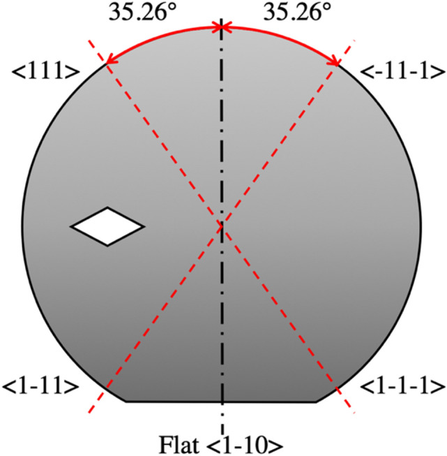
One of the main new ideas we introduced in our new approach is the exploitation of the silicon structural planes with orientation <111>. We fabricated our holes on 100 mm, 525 μm thick wafers with Si <110> crystalline orientation. These wafers have a crystalline orientation such that one of the <111> plane is perpendicular to the surface, tilted by 35.26° with respect to the main flat. We then designed a mask which has rhomboidal structures, whose edges line up with the <111> plane of the crystalline silicon wafer underneath them. In order to have a clear understanding of the etching process, different hole configurations were analyzed: the rhomboidal hole structures had major diagonal size ranging from 1.5 μm (hence with nominal minor diagonal of 1.06 µm) to 20 μm (with nominal minor diagonal of 14.14 µm), and the pitch between neighboring holes was as small as 1.2 times the major diagonal and as large as 5 times.
An oxide layer was used as hard mask: wet oxidation was performed to obtain 1.7 μm thick SiO2 layer. Despite not the best mask in terms of selectivity, which means a sub-optimal maximum achievable aspect ratio, the SiO2 hard mask was thick enough to ensure a good aspect ratio while avoiding the complication and further optimization, which is out of the scope of this paper. The wafer was then coated with 600 nm of AZ ECI 3007 positive tone photoresist and patterned by i-line (λ = 365 nm) photolithography using a Süss MA-6 Gen 3 mask aligner and a chromium mask. The mask was designed in repeated dices fashion (as can be shown from Fig. 1), where both diameter and density factor were swept in each dice. The pattern was then transferred to the SiO2 hard mask by means of fluorine plasma etching. The holes in the silicon substrate were etched by means of the Bosch process12 using an Alcatel AMS 200 dielectric and silicon etcher system.
Figure 1.

Wafer crystalline orientation of the <111> planes for the <110> -type silicon wafers used for the experiments.
The Bosch process is based on alternating depassivation, etch and repassivation steps, using SF6 etching plasma and C4F8 coating gas, pulsed at 6 and 2 s respectively. In our experiments, we achieved a relatively high aspect ratio (AR = 10:1) and lightly tapered holes with evident scalloping roughness on the walls.
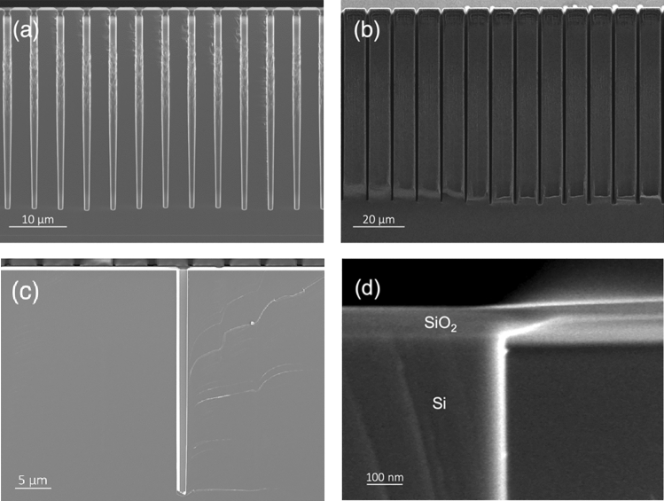
An alternative and more optimized process has been developed by means of a modified Bosch process. As presented by Xu et al.13, we added a cleaning step of O2 plasma between passivation and depassivation steps, in order to clean the excess passivation left over after the plasma etching. The addition of this extra step, the use of a lower chamber pressure, higher plasma bias power and lower chamber temperature of 0 °C, as well as the ramping14 of process parameters (see Table 1) resulted in a much sharper deep reactive ion etching process, with less rough walls and comparable etching rate to the room temperature process, which reached holes with aspect ratios as high as 28:1 and deep trenches with aspect ratios of 75:1 (see Fig. 2). We did not notice any particular effect in terms of maximum hole depth with respect to different pitch variations. However, we are well aware that there is still room for improvement in our etching fabrication step of the process. Nevertheless, although high aspect ratio is essential for the optimization of a TSV technology process, this particular aspect of the process goes beyond the scope of this work.
Table 1.
Parameters of the DRIE etching process.
| Process | ICP power (W) | Cycle (s) | Gas | Flow rate (sccm) | RF power (W) | Pressure (mbar) |
|---|---|---|---|---|---|---|
| Standard DRIE (20°) | ||||||
| Passivation | 1800 | 2 | C4F8 | 300 | 45 | 4 |
| Etching | 1800 | 6 | SF6 | 300 | 45 | 4 |
| Ramping DRIE (0°) | ||||||
| Passivation | 1500 | 2–3 | C4F8 | 300 | 90–110 | 0.4 |
| Depassivation | 1500 | 1 | O2 | 100 | 90–110 | 0.4 |
| Etching | 1500 | 3–5 | SF6 | 300 | 90–110 | 0.4 |
Figure 2.
Scanning electron micrograph of TSV holes (a) and trenches (b) fabricated with the optimized deep reactive ion etching. The width of the hole presents non-negligible bowing effect, going from a minor diagonal size of 1 µm at the top, ~ 1.15 µm in the middle and 0.8 µm at the bottom. Scanning electron micrograph of the Michelangelo-processed TSV hole with an AR of 28:1 (c). After KOH etching, bowing in drastically reduced, giving a slightly wider but constant 1.1 µm minor diagonal width at the top and middle of the TSV, dropping to 1 µm at the bottom. Particular of the surface roughness of the TSV after Michelangelo process (d).
Parasuraman et al.14 show the results of fabrication of deep silicon trenches with an aspect ratio of 160:1 by extreme process optimization and trench sizes as small as 250 nm. The authors show how the achievable aspect ratio increases with smaller feature size. Other interesting results were presented by Owen et al.15 achieving an aspect ratio of 97:1 with trenches as large as 3 μm and by Xu et al.13 where the authors achieved an aspect ratio of 31.4:1 with 12 μm trenches. Despite close but not higher than these highly optimized values, which require use of ramping parameters of DRIE process, it has to be noted that the optimization of the etching process is important but not the ultimate goal of this work, which aims at presenting a way of removing scalloping and tapering effects in holes after a Bosch process. Also, to be noted is that, differently from previous works, we have optimized the etching parameters for holes and not for trenches, which present a much smaller gas inlet while compared to long trenches. The Knudsen transport model16 is even more limiting for holes than it is for trenches, which explains the large differences in achievable aspect ratio using the same process, as confirmed by previous works (see Table 2).
Table 2.
Comparison of several deep reactive ion etching processes.
| Work | Typical size (µm) | Aspect ratio | AR/Size (µm−1) | Etching process |
|---|---|---|---|---|
| H. Li et al. (2018)17 | 100 | 10:1 | 0.10 | DRIE |
| Y. Li et al. (2019)18 | 30 | 10:1 | 0.33 | Modified DRIE |
| Tillocher et al. (2007)19 | 14 | 15:1 | 1.07 | Cryo-etching |
| Shen et al. (2017)1 | 2 | 15:1 | 7.5 | DRIE |
| Motoyoshi et al. (2009)2 | 1.4 | 20:1 | 14.3 | DRIE |
| Fischer et al. (2012)20 | 20 | 24:1 | 1.2 | DRIE |
| This work | 1 | 28:1 | 28 | Modified DRIE |
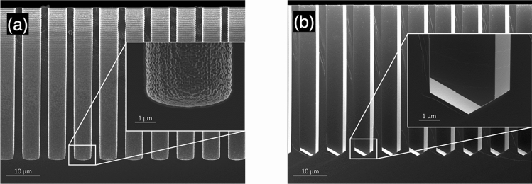
At this step, after the fabrication of the hole with classical methods, we add a surface polishing step consisting of a bath of potassium hydroxide (KOH) solution at 40% heated to 60 °C, which we call the Michelangelo step. By aligning the edges of our rhomboidal patterned holes to the <111> plane of the Si <110> wafer, the KOH step only acts on the scalloping roughness and the taper effects of the fabricated holes, while avoiding measurable lateral etching to the walls. On the bottom end of the hole, other <111> planes are met by the KOH, which is what gives the pyramidal shape that can be shown in Fig. 3. Typical etching times range from a few minutes to almost an hour, due to the different aspect ratios and hole sizes. We believe that the difference there might be related to the microfluidic infiltration of the KOH solution, which becomes more relevant for very small holes with large wall roughness. However, as the lateral etching of the vias is negligible after the exposure of the <111> plane, we decided to etch for 45 to 60 min to ensure reproducibility. After cleaning the hole by the "excess" silicon, the wafer is first put into a HCl bath for potassium particle removal, and then into a buffered hydrofluoric acid (BHF) bath at room temperature for the removal of the excess SiO2 hard mask.
Figure 3.
Scanning electron micrograph of TSV holes fabricated without (a) and with (b) the Michelangelo step. These holes here are 5 µm wide and 40 µm deep: at this aspect ratio, both scalloping and tapering effects are completely removed after immersing the wafer for 60 min in a potassium peroxide bath solution at 40% heated up to 60 °C.
Metallization follows, with deposition of a barrier layer of 50 nm of alumina (Al2O3) deposited by atomic layer deposition using a Beneq TFS200. The two reacting precursors, trimethylaluminum (TMAl) and water, are pulsed in the chamber, heated to 200 °C, to allow consecutive single atomic layer depositions of Al2O3. The seed layer, a thin film of 20 nm of platinum (Pt), was deposited with the same technique in the same machine using as precursors (trimethyl)methylcyclopentadienylplatinum (chemical formula (CH3)3(CH3C5H4)Pt) preheated at 75 °C and O2 reacting in the chamber at 280 °C. Then, to finalize the metallization step, copper electroplating was performed on the samples by an external company (T-Micro, www.t-microtec.com) in non-optimized, standard conditions; the current density used for the Cu electroplating was 0.2 A/dm2 for 50 min.
Results and discussion
We performed TSV fabrication on Si <110> wafers both with and without the proposed wall polishing step. The depth obtained after the deep reactive ion etching was not equal for all hole sizes because the etching rate slows down with increasing aspect ratio: this effect is commonly known as Aspect Ratio Dependent Etching (or ARDE)21.
Figure 3 shows the remarkable results obtained with and without our Michelangelo step. It is evident that, together with any effect related to the wall scalloping, also the effect of tapering in the hole disappears after KOH anisotropic etching.
The Michelangelo step allows polishing of vertical walls on every silicon wafer that has vertical <111> direction perpendicular to the plane of the wafer, such as the Si <110> that we used in this work. Proper design of the hole geometry has then to be considered when changing the silicon wafer crystalline orientation.
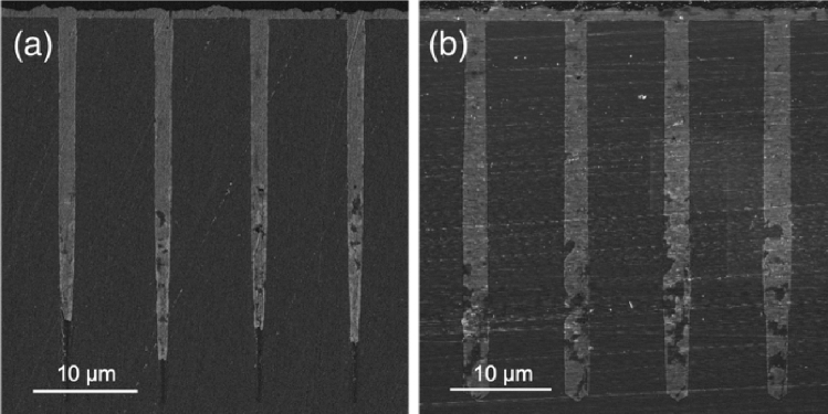
The complete removal of scalloping on the side walls of TSVs allows for better fabrication, since the polished walls prevent unwanted effects, such as stress and electric field concentration. Moreover, it helps with the deposition of insulating and seed layers when using deposition techniques different from atomic layer deposition, such as low-pressure chemical vapor deposition (LPCVD). As shown in Fig. 4, the absence of scalloping and tapering effects allows also a better Cu electroplating step, with a more conformal plating in Through-Silicon Vias with high aspect ratio (AR > 15).
Figure 4.
Scanning electron micrograph of finished TSVs fabricated without (a) and with (b) the Michelangelo step. The two wafers were cut and side-polished to obtain sub-50 nm roughness. Then, for clearer SEM imaging, the sides of the dices were coated with a 13 nm thin carbon film. The apparent difference in aspect ratio between the two images is due to the position of the cut, which was very challenging to align in the very center of the hole in both cases.
In CMOS fabrication one prefers the use of Si <100> wafers for their better silicon dioxide quality. Having a lower silicon atom density at the surface of the silicon–silicon dioxide interface leads to a lower amount of dangling bonds which, in turn, leads to higher carrier mobility. For this reason, the impact of our Michelangelo technology on the CMOS industry may be reduced.
However, this does not apply for other silicon technologies, such as development of top layers of 3D integrated imaging sensors such as APDs, CMOS image sensors (CIS), SPADs and other technologies, or even superconducting circuits technology, such as, for instance, rapid single flux quantum (RSFQ) electronics. Moreover, it is possible to apply a variation of this process while dealing with non-Si technologies, such as InP, InGaAs and other III-V technologies.
Conclusions
We presented the effect of an additional fabrication step, which allows an extremely effective polishing of the TSV’s walls fabricated on Si <110> wafers. Scalloping removal might have a relevant impact for the yield of high aspect ratio TSVs. Future work will focus on characterization of the electro-thermo-mechanical advantages of such process compared to traditional TSV etching processes.
The name of Michelangelo step is related to the famous quote by Michelangelo Buonarroti:
The sculpture is already complete within the marble block, before I start my work.
It is already there, I just have to chisel away the superfluous material.
Indeed, with the final KOH etching step, we just selectively remove all that is superfluous, i.e. the scalloping and the tapering.
Acknowledgments
The authors gratefully acknowledge the staff of the Center of Micro Nanotechnology (CMi) at EPFL, in particular J. Pernollet, C. Hibert and D. Bouvet for discussions regarding etching and thin film atomic layer deposition used to coat the wafer; we also acknowledge the staff of the Center of Electron Microscopy (CiMe) at EPFL, in particular F. Bobard, D. Laub and M. Cantoni, for fruitful discussions regarding the imaging process. The authors also thank the journal reviewers for the fruitful advices. The authors acknowledge financial support from the Swiss National Science Foundation through the Sinergia programme (Grant No. 177165, 2018–2022).
Author contributions
S.F., S.C. and E.C. conceived the idea. S.F. designed the microfabrication process. S.F. and R.C.L. performed the fabrication of the devices. S.F. and B.P. optimized the deep reactive ion etching process. S.F., R.C.L., B.P., I.N.A. and G.F.M.T. performed data acquisition. S.F. and G.F.M.T. analyzed the data. S.F., S.C. and E.C. wrote the paper.
Competing interests
The authors declare the following competing financial interest(s): a U.S. patent application (serial number 63/020,147) based on the reported technology was filed on May 5, 2020 by S.F., R.C.L., S.C. and E.C. through EPFL.
Footnotes
Publisher's note
Springer Nature remains neutral with regard to jurisdictional claims in published maps and institutional affiliations.
References
- 1.Shen W-W, Chen K-N. Three-dimensional integrated circuit (3d ic) key technology: through-silicon via (tsv) Nanoscale Res. Lett. 2017;12(1):56. doi: 10.1186/s11671-017-1831-4. [DOI] [PMC free article] [PubMed] [Google Scholar]
- 2.Motoyoshi M. Through-silicon via (tsv) Proc. IEEE. 2009;97(1):43–48. doi: 10.1109/JPROC.2008.2007462. [DOI] [Google Scholar]
- 3.Gambino JP, Adderly SA, Knickerbocker JU. An overview of through-silicon-via technology and manufacturing challenges. Microelectron. Eng. 2015;135:73–106. doi: 10.1016/j.mee.2014.10.019. [DOI] [Google Scholar]
- 4.Sekiguchi, M. et al. Novel low cost integration of through chip interconnection and application to cmos image sensor. in 56th Electronic Components and Technology Conference, 8 (2006).
- 5.Killge S, Neumann V, Bartha JW. Copper-Based TSV: Interposer. New York: Springer; 2016. pp. 9–28. [Google Scholar]
- 6.Wei T, et al. Optimization and evaluation of sputtering barrier/seed layer in through silicon via for 3-d integration. Tsinghua Sci. Technol. 2014;19(2):150–160. doi: 10.1109/TST.2014.6787368. [DOI] [Google Scholar]
- 7.Lin P, et al. Effects of silicon via profile on passivation and metallization in tsv interposers for 2.5d integration. Microelectron. Eng. 2015;134:22–26. doi: 10.1016/j.mee.2015.01.008. [DOI] [Google Scholar]
- 8.Ranganathan N, et al. Influence of bosch etch process on electrical isolation of tsv structures. IEEE Trans. Comp. Packag. Manuf. Technol. 2011;1(10):1497–1507. doi: 10.1109/TCPMT.2011.2160395. [DOI] [Google Scholar]
- 9.Sasaki M, Li Y, Akatu Y, Fujii T, Hane K. Anisotropically etched Si mold for solid polymer dye cavity laser. Jpn. J. Appl. Phys. 2000;39:7145–7149. doi: 10.1143/JJAP.39.7145. [DOI] [Google Scholar]
- 10.Yun S-S, You S-K, Lee J-H. Fabrication of vertical optical plane using DRIE and KOH crystalline etching of (1 1 0) silicon wafer. Sens. Actuators. A Phys. 2006;128(2):387–394. doi: 10.1016/j.sna.2006.02.015. [DOI] [Google Scholar]
- 11.Lipson A, Yeatman EM. A 1-D photonic band gap tunable optical filter in (110) silicon. J. Microelectromech. Syst. 2007;16(3):521–527. doi: 10.1109/JMEMS.2007.892894. [DOI] [Google Scholar]
- 12.Laermer F. & Schilp, A. Patents US 5501893 and EP 625285 (1996).
- 13.Xu T, Tao Z, Li H, Tan X, Li H. Effects of deep reactive ion etching parameters on etching rate and surface morphology in extremely deep silicon etch process with high aspect ratio. Adv. Mech. Eng. 2017;9(12):1–19. [Google Scholar]
- 14.Parasuraman J, et al. Deep reactive ion etching of sub- micrometer trenches with ultra high aspect ratio. Microelectron. Eng. 2014;113:35–39. doi: 10.1016/j.mee.2013.06.010. [DOI] [Google Scholar]
- 15.Owen, K.J., Van Der Elzen, B., Peterson, R.L. & Najafi, K. High aspect ratio deep silicon etching. In IEEE 25th International Conference on Micro Electro Mechanical Systems (MEMS), 251–254 (2012).
- 16.Coburn JW, Winters HF. Conductance considerations in the reactive ion etching of high aspect ratio features. Appl. Phys. Lett. 1989;55(26):2730–2732. doi: 10.1063/1.101937. [DOI] [Google Scholar]
- 17.Li H, et al. Fabrication and optimization of high aspect ratio through-silicon-vias electroplating for 3d inductor. Micromachines. 2018;9(10):528. doi: 10.3390/mi9100528. [DOI] [PMC free article] [PubMed] [Google Scholar]
- 18.Li Y, et al. Fabrication of sharp silicon hollow microneedles by deep-reactive ion etching towards minimally invasive diagnostics. Microsyst. Nanoeng. 2019;5(1):41. doi: 10.1038/s41378-019-0077-y. [DOI] [PMC free article] [PubMed] [Google Scholar]
- 19.Tillocher T, et al. Silicon cryo-etching of deep holes. Microelectron. Eng. 2007;84(5):1120–1123. doi: 10.1016/j.mee.2007.01.148. [DOI] [Google Scholar]
- 20.Fischer AC, et al. Very high aspect ratio through-silicon vias (TSVs) fabricated using automated magnetic assembly of nickel wires. J. Micromech. Microeng. 2012;22(10):105001. doi: 10.1088/0960-1317/22/10/105001. [DOI] [Google Scholar]
- 21.Yeom J, Wu Y, Selby JC, Shannon MA. Maximum achievable aspect ratio in deep reactive ion etching of silicon due to aspect ratio dependent transport and the microloading effect. J. Vac. Sci. Technol. B. 2005;23(6):2319–2329. doi: 10.1116/1.2101678. [DOI] [Google Scholar]


