

Nonlinear optical response from a van der Waals interface is modulated and enhanced in twistable boron nitride homostructures.
Abstract
Broken symmetries induce strong even-order nonlinear optical responses in materials and at interfaces. Unlike conventional covalently bonded nonlinear crystals, van der Waals (vdW) heterostructures feature layers that can be stacked at arbitrary angles, giving complete control over the presence or lack of inversion symmetry at a crystal interface. Here, we report highly tunable second harmonic generation (SHG) from nanomechanically rotatable stacks of bulk hexagonal boron nitride (BN) crystals and introduce the term twistoptics to describe studies of optical properties in twistable vdW systems. By suppressing residual bulk effects, we observe SHG intensity modulated by a factor of more than 50, and polarization patterns determined by moiré interface symmetry. Last, we demonstrate greatly enhanced conversion efficiency in vdW vertical superlattice structures with multiple symmetry-broken interfaces. Our study paves the way for compact twistoptics architectures aimed at efficient tunable frequency conversion and demonstrates SHG as a robust probe of buried vdW interfaces.
INTRODUCTION
Optical frequency conversion is a nonlinear process where an electromagnetic (EM) field strongly interacts with materials to generate light at new colors. Processes such as second harmonic generation (SHG), optical rectification, and optical parametric amplification arise exclusively from noncentrosymmetric crystals in the limit where EM fields vary slowly over critical length scales of the system (i.e., the electric-dipole limit) (1, 2). For state-of-the-art tunable light sources, optical information processing, and quantum optics (3–6), a compact solid-state platform with a tunable and efficient nonlinear response is highly desirable. Despite recent progress (7–10), this remains a challenge.
Van der Waals (vdW) heterostructures feature twist angle–dependent crystal symmetry (11) and strong optical nonlinearities (12). In this article, we demonstrate highly tunable nonlinear twistoptics in homostructures of hexagonal boron nitride (BN) by combining twistronic (13) techniques for assembly and control (11, 14, 15) with powerful nonlinear optical probes. We investigate twist angle, layer number and its parity, and pump field wavelength as tuning parameters for second-order nonlinear optical response in these all-BN devices. We simulate the system with a transfer matrix model that incorporates interface and bulk effects in the propagation of coupled pump and second harmonic waves, allowing us to optimize devices for tunability and efficiency.
In contrast to prior works focused on stationery few-layer heterostructures (12, 16, 17) (18), we demonstrate highly tunable and enhanced SHG from a dynamically twistable vdW interface buried inside bulk BN crystals. We show that the bulk SHG response (18, 19) can be precisely engineered by layer number control and tuning of the quadrupolar SHG component and that the dipole-allowed interfacial nonlinearity can be effectively modulated by nanomechanical manipulation. In these microrotator devices, broadband SHG tuning can be achieved over an intensity range an order of magnitude larger than conventional electric field–induced effects occurring within a narrower frequency band (8–10), with promising applications as compact optomechanical transducers and high-energy light sources with variable intensity and polarization. Furthermore, by artificially alternating crystal orientations in BN multilayers, we demonstrate vdW vertical superlattice structures where the second harmonic waves generated at each interface can be coherently harnessed to greatly enhance nonlinear efficiency.
Besides potential technological applications in nonlinear nanophotonics, our results show that SHG can serve as a sensitive and selective probe to deeply buried vdW interfaces within bulk encapsulation layers, as well as twist planes (20) inside an otherwise homogeneous crystal. This work should also be relevant to any experiment or application that incorporates bulk BN as an encapsulation material, as the techniques and modeling ultimately provide a complete, noninvasive means to characterize key characteristics of the crystal stack, such as the alignment state between bulk BN pieces.
RESULTS
SHG from bulk BN crystals and homostructures
Bulk BN crystals follow an AA′ interlayer stacking sequence (21) (Fig. 1A). Thus, a given BN crystal belongs to the centrosymmetric D3d point group if the total number of layers N is even, while BN crystal with odd N belongs to the noncentrosymmetric D3h point group. The second-order nonlinear polarization P2ω from BN can be expressed as a multipole expansion (1, 2), , where χ(2) and are the second-order susceptibility tensors for dipole and quadrupole moments, respectively, and Eω is the pump electric field. In few-layer BN, SHG is observed only in samples with odd N, where broken centrosymmetry results in an allowed dipole moment per unit volume (22). When the BN thickness becomes non-negligible compared with the optical wavelength, thin-film interference results in a gradient of the pump field Eω that breaks net inversion symmetry in the out-of-plane direction (2) (Fig. 1A), such that the quadrupole contribution becomes important. Figure 1B shows an exfoliated BN crystal with N ranging from 121 to 124 layers, as determined by combined atomic force microscopy (AFM) and SHG data (see Materials and Methods). In this sample, the region with nominally even N shows bright SHG despite being centrosymmetric, reflecting the existence of a quadrupole effect. Meanwhile, in regions with an odd number of layers, weaker SHG is observed as a result of interference between dipole and quadrupole contributions.
Fig. 1. SHG from bulk BN crystals and homostructures.
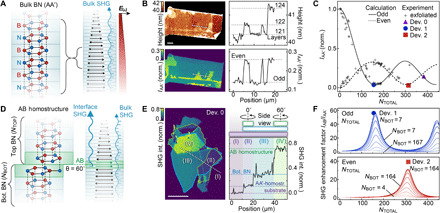
(A) Schematics of crystal structure and bulk SHG (wavy blue arrow) for BN crystal with AA′-stacked layers. Red B (blue N) labels boron (nitrogen) atoms. Black arrows represent nonlinear dipole moments within each layer. Eω denotes pump field. (B) AFM topography (top) and confocal SHG imaging (bottom) of a bulk BN crystal, with corresponding line cuts (right) along the white dashed lines. Scale bar, 5 μm. IAA′ denotes SHG intensity for AA′-stacked BN normalized to that from monolayer BN. (C) IAA′ versus total layer number NTOTAL for AA′-stacked BN. Solid (dashed) lines are nonlinear transfer matrix calculation results for BN with an odd (even) NTOTAL. Gray plus signs (colored markers) represent data for exfoliated BN (AA′ homostructures). (D) Schematic of a BN homostructure with an AB-stacked interface formed by twisting top BN to θ = 60°. Strong dipole-allowed SHG (thick wavy blue arrow) arises from the interfacial bilayer with broken inversion symmetry (green highlight). NTOP (NBOT) denotes the layer number in the top (bottom) BN. (E) SHG image of a BN homostructure. Scale bar, 20 μm. Top right schematic shows top BN (outlined green), comprising two pieces twisted 0° (region II) and 60° (region IV) with respect to bottom BN (outlined blue), all atop a fused silica substrate (outlined purple). SHG intensity along the white dashed line is shown on bottom right, with dashed line guides labeling corresponding regions. (F) SHG enhancement factor IAB/IAA′ as a function of NTOTAL, where IAB is total SHG intensity for AB homostructures. Solid lines are calculation results. Blue (red) dot (square) is experimental data for device 1 (2). Cascading curves separated by 20-layer increments.
The measured SHG from several BN crystals is summarized in Fig. 1C with pump wavelength at 860 nm. The experimental data clearly fall onto two branches, consistent with the dipolar signal’s layer number parity dependence. The data are well described by nonlinear transfer matrix simulations (23) for odd and even layer number N that incorporate the nonlocal multipolar effects (section S1). The phase and magnitude of the quadrupole response vary largely with layer number, forming different interference conditions with the dipole response, as shown by fig. S2. The evolution and reversal of even-odd SHG contrast results from the variation of quadrupole contribution with N, allowing nonlinear response tailoring by layer number engineering. With the layer number parity and SHG linked, we can corroborate layer number estimates for bulk BN as in Fig. 1B. The data in Fig. 1C also include AA′ homostructures made by stacking two exfoliated BN crystals, listed as devices 0 to 2, confirming that the artificially constructed AA′ interface does not give rise to additional SHG.
In a BN-BN homostructure, local symmetry can be broken at the interface by introducing a twist angle θ between the top and bottom crystals. Figure 1D depicts the case of θ = 60°, for which AB interfacial stacking is the lowest energy configuration based on first principles calculations (fig. S3). In AB-stacked BN, boron (nitrogen) atoms in the top BN layer are located right above the nitrogen atoms (hollow sites) of the adjacent BN layer to create a noncentrosymmetric interfacial bilayer. Strong dipole-allowed SHG arises from this interface, in coherent superposition with bulk SHG engineered by layer number N. Figure 1E shows an SHG image of a BN homostructure created by breaking a single N = 192 layer flake, rotating selected pieces by 60° and subsequently stacking to create 2N = 384 layer AA′ and AB homostructures (regions II and IV, respectively), as well as the N layer source crystal (region III). Uniformity of layer number over the majority of regions II to IV was verified by AFM. The AB homostructure shows enhanced SHG due to symmetry breaking, while the AA′ homostructure shows substantially weaker signal despite having the same layer number. To evaluate SHG tunability, we define the SHG enhancement factor IAB/IAA′, where IAB and IAA′ are defined as the SHG intensity from the AB and AA′ homostructure configurations of a given single device. Because SHG sensitively depends on layer number and its even-odd parity, nonlinear transfer matrix calculations are performed for different combinations of top and bottom layer numbers (NTOP and NBOT, with NTOTAL = NTOP + NBOT) for optimized enhancement factor. Figure 1F shows the results for odd and even NTOTAL, with the cascaded curves representing variations of NBOT. More detailed calculations of the dependence on layer number and parity, as well as bulk and interface contributions, are shown by figs. S2 and S4. We find that the interface dipolar SHG can be effectively turned on and off by twisting, while for a set layer number, the bulk SHG remains relatively constant as a function of twist angle. This is sketched in Fig. 1 (A and D), with calculation results in fig. S4. Therefore, large twist angle–dependent SHG tunability can be achieved by selecting layer numbers to maximize the interface contribution and minimize bulk effects.
Tunable SHG from BN microrotators
With an understanding of the SHG response from bulk BN and the buried symmetry broken interface in BN homostructures, we can design nanomechanically rotatable all-BN devices to considerably modulate the SHG response. We tune the interface configuration continuously between the two extremes of AA′ and AB stacking by adjusting the twist angle with an AFM tip (11, 14, 24). Figure 2A illustrates nanomechanical rotation of a BN homostructure to a twist angle of θ, which is defined as a counterclockwise (CCW; as seen from the top) rotation from the AA′ configuration where θ = 0°. Figure 2B shows AFM scans of an assembled rotatable homostructure, comprising an array of bulk BN microrotators atop a larger BN substrate. These can be rotated such that some become crystallographically aligned at extremes that are 60° apart. At these extremes, the rotators become locked and can no longer be rotated by further pushing. The locking behavior is illustrated with schematics and corresponding AFM images by fig. S6. Locking occurs when the interface is twisted to be at AA′ and AB stacking and may be explained by enhanced interlayer friction at these lowest-energy stacking configurations. As shown by Fig. 2 (C and D), SHG imaging can further reveal whether the locking angles correspond to AA′ or AB interfacial stacking. Depending on the initial placement of the BN rotators during assembly, one can either operate in the θ = 0° to 60° range, where CCW rotation transitions a given rotator from AA′ to AB interface as in device 1, or in the θ = 60° to 120° range, where CCW rotation transitions a given rotator from AB to AA′ as in device 2. The uniqueness of twist configuration over a 120° interval that respects the handedness of the twist angle definition is consistent with the threefold rotational symmetry of the bulk BN lattice.
Fig. 2. Dynamical tuning of SHG from BN microrotators.
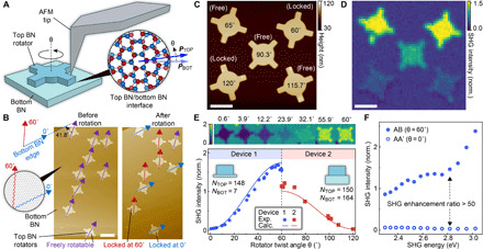
(A) Schematic of a top BN rotator pushed by an AFM on bottom BN. Inset illustrates a top view of the interface at twist angle θ. Blue arrows represent tunable nonlinear dipole moments. (B) AFM images of BN rotators dialed to locking positions at 0° (blue arrows) and 60° (red arrows) with respect to bottom BN. Bottom BN edge (blue dashed line) is parallel to a crystallographic direction of the bottom BN (illustration, left). Purple arrows indicate orientations of freely rotatable top BN. Scale bar is 5 μm. (C) AFM image and (D) SHG image of BN rotators dialed to different twist angles. Scale bars in (C) and (D) are 3 μm. (E) SHG intensity versus θ data for device 1 (blue dots) and device 2 (red squares), with calculated trends (solid lines) and layer numbers indicated by insets. SHG images for rotation states θ < 60° shown above. (F) Energy-dependent SHG intensity for AB (θ = 60°, solid markers) and AA′ (θ = 0°, open markers) interfacial configurations. Data in (D) to (F) normalized to monolayer BN SHG intensity at 2.88 eV.
Figure 2E shows the tuning of SHG intensity with twist angle θ for two devices, each with different thicknesses and therefore different ranges in SHG intensity modulation. Despite large differences in their bulk thicknesses, both devices 1 and 2 exhibit behavior consistent with the changing interface symmetry—highest (lowest) SHG is observed at close to AB (AA′) interface configuration. An SHG modulation enhancement greater than 50 can be achieved between AB and AA′ interface configurations. For comparison, this is about 10 times larger than achievable by electrical tuning mechanisms based on third-order susceptibilities in plasmonic cavities (8) and excitonic SHG from tunable oscillator strength in monolayer semiconductors (9, 25). Moreover, the high tunability of SHG intensity persists over a broad band of frequencies in the visible spectrum, covering at least several hundred millielectron volts as shown by Fig. 2F. The operation frequency window is more than an order of magnitude wider than in devices relying on plasmonic or excitonic resonances (8, 9). Furthermore, the SHG intensity for an AB interface increases substantially at higher energy, entirely consistent with a predicted exciton-influenced smaller optical bandgap as compared with the native AA′-stacked BN crystal (26–29).
Nonlinear optics can serve as an accurate and selective probe of deeply buried interfaces (30). For BN rotators with minimized bulk SHG, the infrared pump beam penetrates the entire structure, and the reflected SHG reports information from the symmetry-broken interface, as illustrated by Fig. 3A. Moreover, the polarization patterns of SHG directly reflect the point group of the lattice (1, 2) and have been relied upon to understand properties of moiré lattices in vdW heterostructures (31). We can therefore probe the tunable moiré symmetry at the deeply buried vdW interface by examining polarization-resolved SHG from the microrotators. Figure 3B illustrates the unit cell of the moiré pattern formed by the interfacial bilayer BN near AB stacking, which belongs to the noncentrosymmetric D3 point group. With broken inversion symmetry, the electric dipole moment plays the dominant role in SHG from the bilayer interface. The nonvanishing elements of the χ(2) tensor responsible for in-plane polarization are −χ(2)xxx = χ(2)xyy = χ(2)yxy = χ(2)yyx (1). In our measurements where pump and SHG collection are collinearly polarized, a sixfold polarization pattern is expected since the SHG intensity varies as ISHG, // ∝ cos2(3(θPOL − θM)), where θPOL is the light polarization angle in the laboratory frame, and θM is the moiré angle defined here as orientation of the three equivalent C2 axes (Fig. 3B). The interfacial moiré patterns and experimental SHG polarization patterns from microrotators are compared in Fig. 3 (C and D) over a broad range of twist angle θ. The above equation is fit to the polarization data measured from devices 1 and 2. The measured SHG symmetry angle θSHG is found to closely follow the expected moiré angle that evolves as θ/2.
Fig. 3. Probing tunable crystal symmetry by polarization resolved SHG.
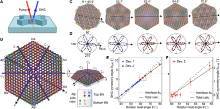
(A) Schematic of SHG as a selective probe to a symmetry-broken interface. (B) Moiré unit cell formed by the interfacial bilayer at θ = 63°, with rotational invariance along three in-plane C2 axes as labeled (left and right) and an out-of-plane C3 axis (right). Side view of AB-stacked BN site, encoding top (bottom) boron as red (green) circles and top (bottom) nitrogen as blue (orange) circles (lower right). (C) Interface moiré patterns and (D) corresponding measured SHG polarization patterns at various twist angles θ. Arrows θM in (C) indicate one of the three C2 axes of the moiré pattern as shown by (B). Blue (red) dots (squares) are measured from device 1 (2). Arrows θSHG indicate the SHG symmetry angle determined from the fit of the polarization data displayed (solid line). (E) Measured θSHG as a function of rotator twist angle θ. Dashed line follows θSHG = θM as the expected trend for the interfacial bilayer. Solid line shows nonlinear transfer matrix calculation results involving the entire bulk structure. (F) Device 2 data near 60° [black dashed box in (E)].
Far from θ = 60°, a deviation is observed between θSHG and θM, as shown by Fig. 3E. The difference is attributed to finite residual bulk SHG, which can be included in the transfer matrix calculation that accounts for the entire structure. By tuning the layer number of the top and bottom BN crystals, we minimize the bulk contribution to be about 2% for device 1 and 4% for device 2, as shown by fig. S3. However, at small twist angle, θ = 60° to 61.2°, the SHG symmetry angle is found to remain at a constant value as shown by the zoom-in plot of Fig. 3F. The bilayer moiré model and the transfer matrix model shown here both assume a rigid lattice for the BN, and neither successfully predicts the pinning of polarization symmetry in this range. On the other hand, the BN interface is likely subject to mechanical relaxation when the twist angle is close to alignment, between 60° and 61°, as verified by calculations of stacking energy and moiré domain area as a function of twist angle, for the simplified case of bilayer BN (see section S9 and fig. S12). Lattice relaxations and soliton formation have also been observed in buried mismatched planes within bulk BN crystals (20). Recent work on BN/graphene heterostructures also shows changes of SHG upon a commensurability transition induced by thermal annealing (18). Therefore, we hypothesize that interfacial atomic reconstruction may explain the constant SHG polarization angle in this range.
SHG enhancement in BN vertical superlattices
Building on the results from BN rotators, one can imagine a multilayered vdW superlattice structure where the crystal orientation of BN is artificially reversed in every other period. As shown by Fig. 4A, multiple AB interfaces between BN thin films can be coherently coupled within the phase-matching limit to enhance SHG intensity. The vertical superlattice structure may provide efficient solutions for applications in frequency-converted light sources, nonlinear optical information processing, and spontaneous downconversion for generating entangled photon pairs (5, 7). The structures are assembled by lithographically cutting a BN crystal with odd layer number N and stacking the pieces with AB interfacial orientation (see Materials and Methods). Figure 4B shows lithographically patterned pieces of a BN crystal with N = 25, and Fig. 4C shows the stacked sample with regions of different numbers of bulk BN crystals layered on top of one another. Figure 4D shows confocal SHG imaging of the resulting structure shown in Fig. 4C. Owing to the coherent superposition between neighboring layers, the SHG field amplitudes from multiple interfaces are added up, and thus, the SHG intensity grows superlinearly with the number of AB interfaces (Fig. 4, D and E). The growing trend of SHG intensity is also theoretically modeled using the nonlinear transfer matrix calculation. The SHG intensity is increased by more than an order of magnitude with homostructure stacks consisting of four BN crystals, measuring a total of 33 nm in thickness, i.e., only about 2% of the SHG pump wavelength. The trend becomes saturated in thicker devices due to the onset of phase mismatch, which could be overcome by using a quasi–phase-matched structure (3) using twist and layer number.
Fig. 4. SHG intensity enhancement by coupling multiple bulk BN crystals.
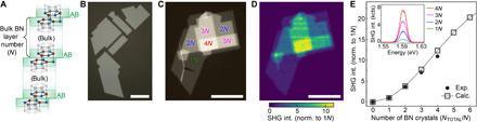
(A) Schematic for a stack of aligned N-layered bulk BN crystals separated by AB interfaces. (B) Optical image of lithographically patterned BN crystal on fused silica. (C) Optical and (D) confocal SHG image of a device assembled from patterned BN shown in (B) featuring regions with 1N to 4N layer thicknesses (N = 25), indicated with colored labels. Scale bars for (B) to (D) are all 10 μm. (E) Scaling of SHG intensity as a function of the number of aligned bulk BN crystals in the stack. Data are normalized to intensity from the 1N layer region. Solid circle markers are experimental data, and open square markers are calculation results. Inset shows SHG emission spectra from regions of different thickness.
DISCUSSION
In conclusion, nonlinear twistoptics in deeply buried symmetry-broken vdW interfaces are demonstrated for highly tunable nonlinear optical applications. In rotatable BN homostructures, the twist angle and the underlying moiré interface are dynamically controlled by nanomechanical means, resulting in symmetry tuning of the interfacial lattice and, hence, drastically modulated SHG. The enhanced SHG arising from the interface in an optimally designed BN homostructure proves to be a sensitive reporter of twist angle–dependent crystal and optoelectronic properties at the buried interface. With the rapid development in wafer-scale growth of single-crystal BN (32–34) and large area disassembly and reassembly techniques (35), we envision that the prototypical demonstrations provided here can be scaled up to further enhance nonlinear efficiency and open new possibilities for compact optical microelectromechanical systems.
MATERIALS AND METHODS
All BN homostructures are assembled using established dry-transfer vdW assembly techniques with a poly-propylene carbonate (PPC) film on a polydimethyl siloxane stamp (36), using a high-precision rotation stage (15). Rotatable structures are fabricated and then mechanically actuated using techniques and processes that are identical to those described in detail in (11, 14), sans graphene processing steps. To minimize possible residue contaminations (37), we note that the surfaces that form the interface in these structures do not come into contact with the PPC, as the transfer polymer only touches the top surface of the top flake, and the surrounding exposed regions of the bottom flake during transfer. In the case of the sample featured in Fig. 4, for which the source BN was lithographically defined using a polymethyl methacrylate (PMMA) mask, the residues were removed using oxygen-argon annealing (38) before vdW assembly. Unless otherwise mentioned, all devices and exfoliated samples rest atop a fused silica substrate for study. The bottom BN in device 4 appearing in section S3 and figs. S2 and S4 was exfoliated using large-area disassembly techniques (35). The crystallographic orientations of the top BN rotator and the bottom BN substrate are predetermined by performing polarization-resolved SHG before the assembly (fig. S5). Straight edges of bulk BN crystals that are found to be typically aligned with either the armchair or zigzag orientation serve as references for defining the straight arms of the rotators.
For SHG measurements, a Ti:sapphire femtosecond pulsed laser and optical parametric oscillator are used as pump sources, with typical power on the order of a few milliwatts. An objective with numerical aperture of 0.95 is used for confocal imaging, with a typical beam spot diameter of about 550 nm. For accurate measurement of nonlinear intensity, each sample is always piezo scanned along the z-direction to optimize focus. An electron-multiplying charge-coupled device is used for fast signal collection with spectral resolution. For a complete diagram of the measurement setup, see fig. S13.
For the bulk BN thickness and layer number parity-dependent BN measurements shown in Fig. 1 (B and C), the thickness (t) with corresponding layer number (N = t/0.334) of a given BN crystal is measured from AFM scans. The uncertainty in thickness measurements of a given bulk flake BN is estimated to be ±0.5 nm. Confocal SHG measurements for mono-to-few layer steps on the top surface of the BN crystal (corresponding to measured total thickness NTOTAL = ..., N − 2, N − 1, N, N + 1, N + 2,...) are compared with the prediction given by the nonlinear transfer matrix calculations, which allows us to assign the layer number parity for the given region based on our model and, therefore, the layer number parity of N.
Angle measurements of BN micromechanical rotators are extracted from AFM scans using a digital protractor. The twist angle θ between a given BN rotator and the bottom BN is assigned on the basis of its angle relative to the locked rotators that are 60° apart from one another. Assignment of θ for the locked rotators is given through a comparison of the measured SHG intensity from each rotator and the calculated prediction for AA′- and AB-stacked bulk-on-bulk BN with comparable thicknesses. Locking is determined by observing an inability to continue pushing the BN rotator without physically damaging it with the AFM tip. Further details regarding this locking behavior are provided in section S5 and fig. S6.
Acknowledgments
We thank D. Xiao and J. Wang for the helpful discussions and technical support. Funding: This research is mainly supported as part of Programmable Quantum Materials, an Energy Frontier Research Center funded by the U.S. Department of Energy (DOE), Office of Science, Basic Energy Sciences (BES), under award DE-SC0019443. Theory support involving DFT calculations for this project is supported by the European Research Council (ERC-2015-AdG694097), the Cluster of Excellence AIM, and the Max Planck Institute–New York City Center for Non-Equilibrium Quantum Phenomena (A.R.). The Flatiron Institute is a division of the Simons Foundation. N.F. acknowledges support from the Stewardship Science Graduate Fellowship program provided under cooperative agreement number DE-NA0003864. K.W. and T.T. acknowledge support from the Elemental Strategy Initiative conducted by the MEXT, Japan (grant number JPMXP0112101001), JSPS KAKENHI (grant number JP20H00354), and the CREST (JPMJCR15F3), JST. J.Z. acknowledges funding received from the European Union Horizon 2020 research and innovation program under the Marie Sklodowska-Curie Grant Agreement 886291 (PeSD-NeSL). Author contributions: K.Y. and N.R.F. performed the measurements and analyzed the data. K.Y., J.Z., L.X., N.T.-D., D.H., H.O., A.A.-G., and A.R. performed the theory calculations. N.R.F. fabricated all the devices. F.L. assisted with sample preparation. S.L.M., J.A., and X.X. assisted with preliminary experimental efforts. K.W. and T.T. grew the BN crystals. H.O., A.A.-G., X.Z., D.N.B., A.R., C.R.D., J.H., and P.J.S. advised on the experiments. The manuscript was written with input from all authors. Competing interests: F.L., X.Y.Z., and J.H. are inventors on a patent application related to this work filed by Columbia University (no. 62/944,753 and 62/963,839, filed 6 December 2019). The authors declare that they have no other competing interests. Data and materials availability: All data needed to evaluate the conclusions in the paper are present in the paper and/or the Supplementary Materials. All data generated and analyzed during this study are available from the corresponding author upon reasonable request. All the custom codes used in this study are available from the corresponding author upon reasonable request.
SUPPLEMENTARY MATERIALS
Supplementary material for this article is available at http://advances.sciencemag.org/cgi/content/full/7/10/eabe8691/DC1
REFERENCES AND NOTES
- 1.Y.-R. Shen, The Principles of Nonlinear Optics (Wiley-Interscience, New York, 1984). [Google Scholar]
- 2.Heinz T. F., Second-order nonlinear optical effects at surfaces and interfaces, in Modern Problems in Condensed Matter Sciences (Elsevier Science Publishers Β.V., 1991), 29, pp. 353–416. [Google Scholar]
- 3.R. W. Boyd, Nonlinear Optics (Elsevier, 2003). [Google Scholar]
- 4.Garmire E., Nonlinear optics in daily life. Opt. Express 21, 30532–30544 (2013). [DOI] [PubMed] [Google Scholar]
- 5.Fiorentino M., Spillane S. M., Beausoleil R. G., Roberts T. D., Battle P., Munro M. W., Spontaneous parametric down-conversion in periodically poled KTP waveguides and bulk crystals. Opt. Express 15, 7479–7488 (2007). [DOI] [PubMed] [Google Scholar]
- 6.Zhang X., Cao Q., Wang Z., Liu Y., Qiu C., Yang L., Gong Q., Xiao Y., Symmetry-breaking-induced nonlinear optics at a microcavity surface. Nat. Photonics 13, 21–24 (2019). [Google Scholar]
- 7.Chang D. E., Vuletić V., Lukin M. D., Quantum nonlinear optics—Photon by photon. Nat. Photonics 8, 685–694 (2014). [Google Scholar]
- 8.Cai W., Vasudev A. P., Brongersma M. L., Electrically controlled nonlinear generation of light with plasmonics. Science 333, 1720–1723 (2011). [DOI] [PubMed] [Google Scholar]
- 9.Seyler K. L., Schaibley J. R., Gong P., Rivera P., Jones A. M., Wu S., Yan J., Mandrus D. G., Yao W., Xu X., Electrical control of second-harmonic generation in a WSe2 monolayer transistor. Nat. Nanotechnol. 10, 407–411 (2015). [DOI] [PubMed] [Google Scholar]
- 10.Chen S., Li K. F., Li G., Cheah K. W., Zhang S., Gigantic electric-field-induced second harmonic generation from an organic conjugated polymer enhanced by a band-edge effect. Light Sci. Appl. 8, 17 (2019). [DOI] [PMC free article] [PubMed] [Google Scholar]
- 11.Finney N. R., Yankowitz M., Muraleetharan L., Watanabe K., Taniguchi T., Dean C. R., Hone J., Tunable crystal symmetry in graphene–boron nitride heterostructures with coexisting moiré superlattices. Nat. Nanotechnol. 14, 1029–1034 (2019). [DOI] [PubMed] [Google Scholar]
- 12.Yao K., Yanev E., Chuang H.-J., Rosenberger M. R., Xu X., Darlington T., McCreary K. M., Hanbicki A. T., Watanabe K., Taniguchi T., Jonker B. T., Zhu, Basov D. N., Hone, Schuck P. J., Continuous wave sum frequency generation and imaging of monolayer and heterobilayer two-dimensional semiconductors. ACS Nano 14, 708–714 (2020). [DOI] [PubMed] [Google Scholar]
- 13.Carr S., Massatt D., Fang S., Cazeaux P., Luskin M., Kaxiras E., Twistronics: Manipulating the electronic properties of two-dimensional layered structures through their twist angle. Phys. Rev. B 95, 075420 (2017). [Google Scholar]
- 14.Ribeiro-Palau R., Zhang C., Watanabe K., Taniguchi T., Hone J., Dean C. R., Twistable electronics with dynamically rotatable heterostructures. Science 361, 690–693 (2018). [Google Scholar]
- 15.Kim K., Yankowitz M., Fallahazad B., Kang S., Movva H. C. P., Huang S., Larentis S., Corbet C. M., Taniguchi T., Watanabe K., Banerjee S. K., LeRoy B. J., Tutuc E., van der Waals heterostructures with high accuracy rotational alignment. Nano Lett. 16, 1989–1995 (2016). [DOI] [PubMed] [Google Scholar]
- 16.Kim C.-J., Brown L., Graham M. W., Hovden R., Havener R. W., McEuen P. L., Muller D. A., Park J., Stacking order dependent second harmonic generation and topological defects in h-BN bilayers. Nano Lett. 13, 5660–5665 (2013). [DOI] [PubMed] [Google Scholar]
- 17.Hsu W.-T., Zhao Z.-A., Li L.-J., Chen C.-H., Chiu M.-H., Chang P.-S., Chou Y.-C., Chang W.-H., Second harmonic generation from artificially stacked transition metal dichalcogenide twisted bilayers. ACS Nano 8, 2951–2958 (2014). [DOI] [PubMed] [Google Scholar]
- 18.Stepanov E. A., Semin S. V., Woods C. R., Vandelli M., Kimel A. V., Novoselov K. S., Katsnelson M. I., Nonlinear optical study of commensurability effects in graphene-hBN heterostructures. ACS Appl. Mater. Interfaces 12, 27758–27764 (2020). [DOI] [PubMed] [Google Scholar]
- 19.Kim S., Froch J., Gardner A., Li C., Aharonovich I., Solntsev A., Second harmonic generation in multilayer hexagonal boron nitride flakes. Opt. Lett. 44, 5792–5795 (2019). [DOI] [PubMed] [Google Scholar]
- 20.Ni G. X., Wang H., Jiang B.-Y., Chen L. X., Du Y., Sun Z. Y., Goldflam M. D., Frenzel A. J., Xie X. M., Fogler M. M., Basov D. N., Soliton superlattices in twisted hexagonal boron nitride. Nat. Commun. 10, 4360 (2019). [DOI] [PMC free article] [PubMed] [Google Scholar]
- 21.Pease R. S., Crystal structure of boron nitride. Nature 165, 722–723 (1950). [DOI] [PubMed] [Google Scholar]
- 22.Li Y., Rao Y., Mak K. F., You Y., Wang S., Dean C. R., Heinz T. F., Probing symmetry properties of few-layer MoS2 and h-BN by optical second-harmonic generation. Nano Lett. 13, 3329–3333 (2013). [DOI] [PubMed] [Google Scholar]
- 23.Bethune D. S., Optical harmonic generation and mixing in multilayer media: Analysis using optical transfer matrix techniques. J. Opt. Soc. Am. B 6, 910–916 (1989). [Google Scholar]
- 24.Chari T., Riberio-Palau R., Dean C. R., Shepard K., Resistivity of rotated graphite–graphene contacts. Nano Lett. 16, 4477–4482 (2016). [DOI] [PubMed] [Google Scholar]
- 25.Yao K., Yan A., Kahn S., Suslu A., Liang Y., Barnard E., Tongay S., Zettl A., Borys N. J., Schuck P. J., Optically discriminating carrier-induced quasiparticle band gap and exciton energy renormalization in monolayer MoS2. Phys. Rev. Lett. 119, 087401 (2017). [DOI] [PubMed] [Google Scholar]
- 26.Ochoa H., Asenjo-Garcia A., Flat bands and chiral optical response of moiré insulators. Phys. Rev. Lett. 125, 037402 (2020). [DOI] [PubMed] [Google Scholar]
- 27.Xian L., Kennes D. M., Tancogne-Dejean N., Altarelli M., Rubio A., Multiflat bands and strong correlations in twisted bilayer boron nitride: Doping-induced correlated insulator and superconductor. Nano Lett. 19, 4934–4940 (2019). [DOI] [PMC free article] [PubMed] [Google Scholar]
- 28.Wirtz L., Marini A., Rubio A., Excitons in boron nitride nanotubes: Dimensionality effects. Phys. Rev. Lett. 96, 126104 (2006). [DOI] [PubMed] [Google Scholar]
- 29.L. Wirtz, A. Rubio, Excitons in Boron Nitride Nanotubes: Dimensionality Effects, in B-C-N Nanotubes and Related Nanostructures (Lecture Notes in Nanoscale Science and Technology 6 Series, New York, Springer, 2009), pp. 105–148. [Google Scholar]
- 30.Shen Y. R., Ostroverkhov V., Sum-frequency vibrational spectroscopy on water interfaces: Polar orientation of water molecules at interfaces. Chem. Rev. 106, 1140–1154 (2006). [DOI] [PubMed] [Google Scholar]
- 31.Y. Bai, L. Zhou, J. Wang, W. Wu, L. McGilly, D. Halbertal, C. F. B. Lo, F. Liu, J. Ardelean, P. Rivera, N. R. Finney, X. Yang, D. N. Basov, W. Yao, X. Xu, J. Hone, A. Pasupathy, X. Zhu, One-dimensional moiré excitons in transition-metal dichalcogenide heterobilayers. arXiv:1912.06628 [cond-mat.mtrl-sci] (2019).
- 32.Lee J. S., Choi S. H., Yun S. J., Kim Y. I., Boandoh S., Park J.-H., Shin B. G., Ko H., Lee S. H., Kim Y.-M., Lee Y. H., Kim K. K., Kim S. M., Wafer-scale single-crystal hexagonal boron nitride film via self-collimated grain formation. Science 362, 817–821 (2018). [DOI] [PubMed] [Google Scholar]
- 33.Wang L., Xu X., Zhang L., Qiao R., Wu M., Wang Z., Zhang S., Liang J., Zhang Z., Zhang Z., Chen W., Xie X., Zong J., Shan Y., Guo Y., Willinger M., Wu H., Li Q., Wang W., Gao P., Wu S., Zhang Y., Jiang Y., Yu D., Wang E., Bai X., Wang Z.-J., Ding F., Liu K., Epitaxial growth of a 100-square-centimetre single-crystal hexagonal boron nitride monolayer on copper. Nature 570, 91–95 (2019). [DOI] [PubMed] [Google Scholar]
- 34.Chen T.-A., Chuu C.-P., Tseng C.-C., Wen C.-K., Philip Wong H.-S., Pan S., Li R., Chao T.-A., Chueh W.-C., Zhang Y., Fu Q., Yakobson B. I., Chang W.-H., Li L.-J., Wafer-scale single-crystal hexagonal boron nitride monolayers on Cu (111). Nature 579, 219–223 (2019). [DOI] [PubMed] [Google Scholar]
- 35.Liu F., Wu W., Bai Y., Chae S. H., Li Q., Wang J., Hone J., Zhu X.-Y., Disassembling 2D van der Waals crystals into macroscopic monolayers and reassembling into artificial lattices. Science 367, 903–906 (2020). [DOI] [PubMed] [Google Scholar]
- 36.Wang L., Meric I., Huang P. Y., Gao Q., Gao Y., Tran H., Taniguchi T., Watanabe K., Campos L. M., Muller D. A., Guo J., Kim P., Hone J., Shepard K. L., Dean C. R., One-dimensional electrical contact to a two-dimensional material. Science 342, 614–617 (2013). [DOI] [PubMed] [Google Scholar]
- 37.Jain A., Bharadwaj P., Heeg S., Parzefall M., Taniguchi T., Watanabe K., Novotny L., Minimizing residues and strain in 2D materials transferred from PDMS. Nanotechnology 29, 265203 (2018). [DOI] [PubMed] [Google Scholar]
- 38.Garcia A. G. F., Neumann M., Amet F., Williams J., Watanabe K., Taniguchi T., Goldhaber-Gordon D., Effective cleaning of hexagonal boron nitride for graphene devices. Nano Lett. 12, 4449–4454 (2012). [DOI] [PubMed] [Google Scholar]
- 39.Carr S., Massatt D., Torrisi S. B., Cazeaux P., Luskin M., Kaxiras E., Relaxation and domain formation in incommensurate two-dimensional heterostructures. Phys. Rev. B 98, 224102 (2018). [Google Scholar]
- 40.Falin A., Cai Q., Santos E. J. G., Scullion D., Qian D., Zhang R., Yang Z., Huang S., Watanabe K., Taniguchi T., Barnett M. R., Chen Y., Ruoff R. S., Li L. H., Mechanical properties of atomically thin boron nitride and the role of interlayer interactions. Nat. Commun. 8, 15815 (2017). [DOI] [PMC free article] [PubMed] [Google Scholar]
- 41.Zhou S., Han J., Dai S., Sun J., Srolovitz D. J., Van der Waals bilayer energetics: Generalized stacking-fault energy of graphene, boron nitride, and graphene/boron nitride bilayers. Phys. Rev. B 92, 155438 (2015). [Google Scholar]
- 42.Kresse G., Furthmüller J., Efficient iterative schemes for ab initio total-energy calculations using a plane-wave basis set. Phys. Rev. B 54, 11169 (1996). [DOI] [PubMed] [Google Scholar]
- 43.Perdew J. P., Burke K., Ernzerhof M., Generalized gradient approximation made simple. Phys. Rev. Lett. 77, 3865–3868 (1996). [DOI] [PubMed] [Google Scholar]
- 44.Klimeš J., Bowler D. R., Michaelides A., Van der Waals density functionals applied to solids. Phys. Rev. B 83, 195131 (2011). [Google Scholar]
- 45.Lee S.-Y., Jeong T.-Y., Jung S., Yee K.-J., Refractive index dispersion of hexagonal boron nitride in the visible and near infrared. Phys. Status Solidi B 256, 1800417 (2019). [Google Scholar]
Associated Data
This section collects any data citations, data availability statements, or supplementary materials included in this article.
Supplementary Materials
Supplementary material for this article is available at http://advances.sciencemag.org/cgi/content/full/7/10/eabe8691/DC1