Conspectus
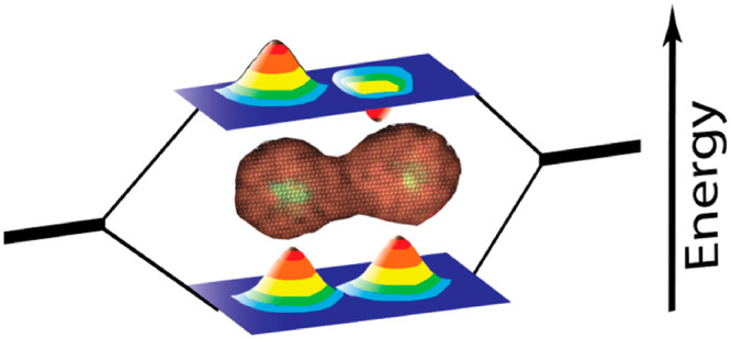
Electronic coupling and hence hybridization of atoms serves as the basis for the rich properties for the endless library of naturally occurring molecules. Colloidal quantum dots (CQDs) manifesting quantum strong confinement possess atomic-like characteristics with s and p electronic levels, which popularized the notion of CQDs as artificial atoms. Continuing this analogy, when two atoms are close enough to form a molecule so that their orbitals start overlapping, the orbitals energies start to split into bonding and antibonding states made out of hybridized orbitals. The same concept is also applicable for two fused core–shell nanocrystals in close proximity. Their band edge states, which dictate the emitted photon energy, start to hybridize, changing their electronic and optical properties. Thus, an exciting direction of “artificial molecules” emerges, leading to a multitude of possibilities for creating a library of new hybrid nanostructures with novel optoelectronic properties with relevance toward diverse applications including quantum technologies.
The controlled separation and the barrier height between two adjacent quantum dots are key variables for dictating the magnitude of the coupling energy of the confined wave functions. In the past, coupled double quantum dot architectures prepared by molecular beam epitaxy revealed a coupling energy of few millielectron volts, which limits the applications to mostly cryogenic operation. The realization of artificial quantum molecules with sufficient coupling energy detectable at room temperature calls for the use of colloidal semiconductor nanocrystal building blocks. Moreover, the tunable surface chemistry widely opens the predesigned attachment strategies as well as the solution processing ability of the prepared artificial molecules, making the colloidal nanocrystals as an ideal candidate for this purpose. Despite several approaches that demonstrated enabling of the coupled structures, a general and reproducible method applicable to a broad range of colloidal quantum materials is needed for systematic tailoring of the coupling strength based on a dictated barrier
This Account addresses the development of nanocrystal chemistry to create coupled colloidal quantum dot molecules and to study the controlled electronic coupling and their emergent properties. The simplest nanocrystal molecule, a homodimer formed from two core/shell nanocrystal monomers, in analogy to homonuclear diatomic molecules, serves as a model system. The shell material of the two CQDs is structurally fused, resulting in a continuous crystal. This lowers the potential energy barrier, enabling the hybridization of the electronic wave functions. The direct manifestation of the hybridization reflects on the band edge transition shifting toward lower energy and is clearly resolved at room temperature. The hybridization energy within the single homodimer molecule is strongly correlated with the extent of structural continuity, the delocalization of the exciton wave function, and the barrier thickness as calculated numerically. The hybridization impacts the emitted photon statistics manifesting faster radiative decay rate, photon bunching effect, and modified Auger recombination pathway compared to the monomer artificial atoms. Future perspectives for the nanocrystals chemistry paradigm are also highlighted.
Key References
Cui J.; Panfil Y. E.; Koley S.; Shamalia D.; Waiskopf N.; Remennik S.; Popov I.; Oded M.; Banin U.. Colloidal Quantum Dot Molecules Manifesting Quantum Coupling at Room Temperature. Nat. Commun. 2019, 10, 5401..1This work reports a general and facile strategy for the synthesis of fused colloidal quantum dots molecules using silica particles as a template with fusion at moderate temperatures. The wave function hybridization was revealed experimentally and computationally showing a red-shift in band-edge, resolvable at room temperature. The coherent tunneling and exciton transfer appear to be the underlying mechanisms.
Panfil Y. E.; Shamalia D.; Cui J.; Koley S.; Banin U.. Electronic Coupling in Colloidal Quantum Dot Molecules; the Case of CdSe/CdS Core/Shell Homodimers. J. Chem. Phys. 2019, 151, 224501..2This work elucidates the influence of the parameters governing electronic coupling in the fused CdSe/CdS homodimer structure. This study provides essential guidelines to rational design of the coupled quantum dot molecules with specific attributes.
Jia G.; Sitt A.; Hitin G. B.; Hadar I.; Bekenstein Y.; Amit Y.; Popov I.; Banin U.. Couples of Colloidal Semiconductor Nanorods Formed by Self-Limited Assembly. Nat. Mater. 2014, 13, 301–307.3This work reports a method for the formation of the coupled semiconductor nanorods based on the oriented attachment. This coupling in nanorods altered the band-edge to the shorter edge and hence the light polarization feature.
1. Introduction
Colloidal quantum dots (CQDs) are semiconductor nanocrystals containing hundreds to thousands of atoms arranged in a crystal structure of the bulk semiconductor.4,5 When the crystal is smaller than the exciton Bohr radius of the semiconductor, the energy levels, especially near the band edge, blue shift and become discrete because of the quantum confinement effect.6−8 This allows one to tune the electron and hole states as a function of size and shape. Core/shell quantum dots are particularly interesting as the shell material passivates the dangling bonds on the surface and the shell acts as an electronic potential barrier for the charge carriers keeping them away from the traps on the surface.9 Extensive studies over last three decades focusing on the structure, surface, and interface achieved superior optical and electronic properties leading to applications of quantum dots in displays, photodetectors, and solar harvesting and as biomarkers to name a few.
How two adjacent CQDs interact in close proximity and the ways to couple the neighboring particles are important questions in realizing nanocrystal based devices. Specifically utilizing the artificial atom character of the quantum dots (to be discussed later), hybridization of the confined wave functions in two dots is anticipated.10 In the following, we present the overview of the latest findings and current progress on CQD molecules. First, a brief introduction of the synthetic strategies, followed by coupling attributes via wave function hybridization in the coupled homodimer CQD molecules, will be discussed. Next, the photophysical aspects of the coupled CQDs, down to single particle level, are presented. Finally, we provide a perspective on the challenges and future opportunities in this field toward potential applications.
2. From Artificial Atom to Artificial Molecules
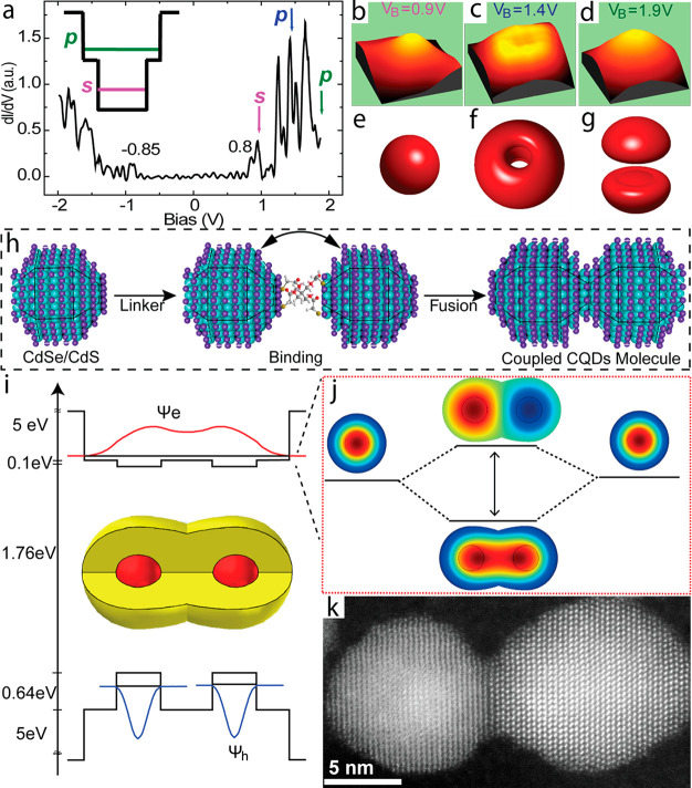
Due to the quantum confinement effect, the CQDs present a transition state between the solid-state and molecular regimes with discrete energy levels and electronic states, and are often described as “artificial atoms”.4 This analogy was clearly revealed experimentally, where the spherical shape CQDs present atomic-like symmetries and degeneracies for the electronic states and wave functions, for example “s” and “p” states.11,12 As depicted in Figure 1a–g, the different extent of the conduction band (CB) s and p states of InAs/ZnSe core/shell nanocrystals were directly probed by scanning tunneling microscopy (STM). Bias-dependent current imaging delineated the atomic-like states of the CQDs by measuring the dI/dV – V spectrum (Figure 1a). Current images at different bias values directly revealed the nature of the s states at lower bias and p states at higher bias (Figure 1b–g).
Figure 1.
(a) Scanning tunneling spectrum acquired for the wave function imaging of InAs/ZnSe core/shell QDs. (b–d) Current images obtained at different bias values denoted by arrows in (a). (e–g) Isoprobability surfaces, showing s2 (e), px2 + py2 (f), and pz2 (g). Adapted from ref (14). Copyright 2001 American Physical Society. (h) Simplified scheme for the synthesis of coupled artificial molecules formed from two core/shell CQDs monomers. Following the formation of dimers connected via organic linker, thermal fusion creates the coupled CQD molecule. (i) Potential energy landscape and cross-section of the calculated first electron and hole wave functions in CdSe/CdS CQD molecules. (j) Calculated bonding and antibonding two-dimensional electron wave functions without Coulombic interaction. (k) HAADF-STEM image for the CQDs homodimer molecule. Adapted from ref (1). Copyright 2019 Springer Nature.
The observations of the artificial atom character of CQDs inspired the formation of quantum dot molecules where the creation of hybridized excitons can impose novel synergistic functionalities, relevant to numerous applications including in quantum technologies. This requires the controlled placement of a second quantum system in close proximity.13 The chemical bond serves as a basis of molecule formation with electronically coupled atomic states, enabling tunneling of the electrons and delocalization throughout the new hybridized molecular state.2 Similarly, close proximity of two quantum dots with a minimal barrier engenders hybridized electron wave function delocalized throughout the double quantum dot structure, forming a quantum molecule. In the following sections, we will describe the advancement, hurdles, and development of a general strategy for coupling two quantum dots into an artificial molecule (Figure 1h).
3. Strategies to Fabricate Artificial Quantum Molecules
The first attempts to hybridize the exciton wave function were made with epitaxially grown and self-assembled quantum dots. The close proximity of two quantum dots led to hybridized wave functions, that respond to perturbation from an external electric field, as studied at single-particle level.15,16 In MBE grown QD molecules, along with the lack of solution processability, cryogenic operation remains a limitation owing to the typically small hybridization energies.11,17,18
For colloidal quantum dots, up to now, the successive ion layer adsorption and reaction (SILAR)-based method was used to form coupled structures such as core–multishells.19,20 Double-QDs at nanorod apexes were also reported.21−23 With controlled precursor reactivity and injection rate, the growth of additional QDs could be tailored on the apex of dot-in-rod structures, for example, and yield a coupled system.21 In these structures, dual emitting nanocrystals were demonstrated via spatial separation of the carrier wave function, with simultaneous interaction of the exciton via dipole or tunnel coupling. Wave function mixing in rod-couples lowering the emission polarization has also been demonstrated.3 Due to the specific materials architectures and types combined with lattice mismatch and surface strain, the precise control of coupling parameters are limited by these strategies.
Utilizing the surface chemistry of the CQDs, dimer and oligomeric structures were prepared using nanoscale templates, including organic polymers,24 biomolecules,25 and nanotemplates (polystyrene and SiO2 particles).26 The linker/templates were utilized to shorten the distance between the building blocks to facilitate interparticle interaction. On top of this, the template-free methods, utilizing dipole–dipole interaction,27,28 ligand exchange,29 solvent evaporation,30 and electrostatic interaction,26 were also used to assemble CQDs in close proximity. The ensemble of closely packed CQDs forming superlattice or molecular-like aggregates manifested the interdot interaction and coherent exciton dynamics at room temperature.31,32 Even with a short cross-linker that minimizes the distance between two CQDs, significant energy barrier is still imposed by the interfacial organic ligands and linkers, restricting the wave function hybridization. However, a dipolar nonradiative resonance energy transfer interaction can still be efficient with time scale down to tens of picoseconds.30,31,33 These reports emphasized the distinct nature of the exciton kinetics compared to isolated quantum system in ambient conditions, driving further the motivation to generate and study isolated colloidal quantum dot molecules.
Fusion of nanocrystals via oriented attachment (OA) provides a solution to this interfacial organic ligand barrier. During OA, a single nanocrystal is formed from two adjacent nanoparticles based on the formation of the atomically matched bond between the two specific facets, governed by the minimization of the highest surface energy of the most reactive facets.34−37 The controlled OA is widely utilized for the formation of nanocrystals with various novel architectures, including nanowire nanochains and helical, branched, and nanorings.24 Various methods have been developed to fuse the nanocrystals via thermal annealing,38 pressure compression,39 and pulsed laser annealing.40 In a vision to hybridize the wave functions, this method was applied recently to Pb-chalcogenide nanocrystals. Notably, Beard and co-workers reported the broadening of the 1S exciton peak owing to wave function hybridization in PbSe fused dimers with a splitting of the degenerate energy levels of up to 140 meV.41 Alivisatos and co-workers have analyzed the possible crystallographic defects at the interface of PbTe42 and CdSe43 nanocrystal arrays due to misfit dislocation, twinning or grain boundaries, and stacking forces. The attachment of the CQD facets forming a continuous lattice eliminates the ligand barrier facilitating the carrier wave function overlap while a rigorous control of the interfacial defects should be addressed. However, the oriented attachment of the nanocrystal facets in free solution often yields uncontrolled higher order oligomeric structures limiting the formation of isolated controlled dimers.
A template based approach overcame these limitations, where the selective dimer preparation is performed on a template, thus reducing the chance of higher order oligomerization with high yield of the desired dimer structures.1 As demonstrated in the following sections, choosing the core/shell CQDs as artificial atoms where the continuous shell lattice embraces the core CQDs eliminates the interfacial ligand barrier while the shell thickness itself defines the barrier height. This general approach offers the ability to prepare the fused nanocrystal molecules with a wide variety of size, structure, and composition, predesigned and tested computationally. As depicted in Figure 1i, the quantum-mechanical calculation for a CdSe/CdS homodimer molecule reveals the hybridization of the 1Se electron wave functions forming bonding and antibonding states with corresponding wave functions presented in the Figure 1j, given by in-phase and antiphase superpositions of the monomer wave functions, respectively (Figure 1k).2
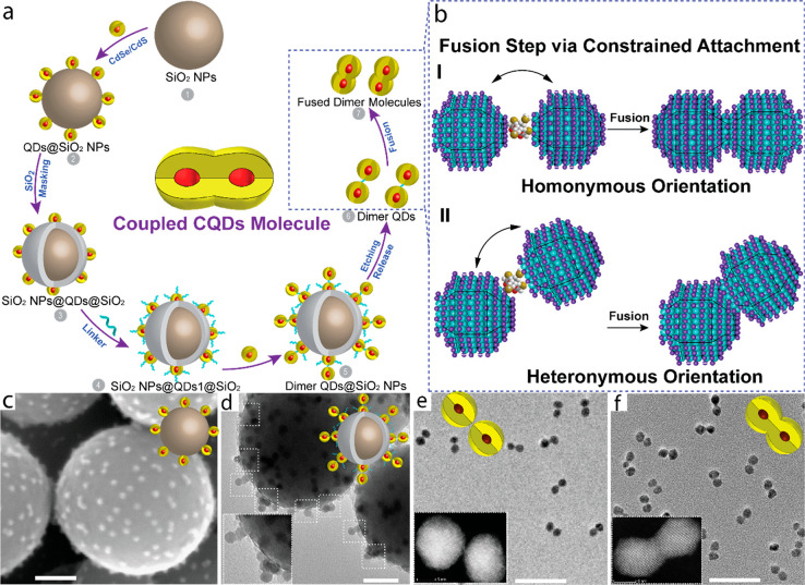
Submicrometer sized nanoshpheres have been utilized as the template as they offer high surface area and flexibility to tune the surface chemistry for anchoring small nanocrystals and manipulating their surface chemical functionality while anchored on the template itself.44,45 The first step for the preparation of the CQD molecules is to prepare a cross-linked CQD dimer on the template (Figure 2a). Surface functionalized silica particles first accommodate the core/shell CQDs (Figure 2c), following the controlled coverage of the unreacted silica anchor sites and a portion of the anchored CQDs. This masking step simultaneously reduces the possibility of both generating unreacted monomers and higher order oligomeric species along with the desired dimer. The second CQD can easily be anchored to the first CQD with a cross-linker precisely, to form a cross-linked homodimer on the template surface (Figure 2d). The dimers are then detached from the template by etching the silica spheres (Figure 2e). These cross-linked homodimers however did not shift the 1S exciton peak lacking the wave function hybridization due to the high energy barrier imposed by the organic ligands and cross-linker at the interface.
Figure 2.
(a) Scheme for the formation of the coupled CQDs molecules utilizing SiO2 particles as template. (b) Structural model for constrained attachment in CdSe/CdS CQD molecules with homonymous and heteronymous plane orientations during fusion. TEM images of (c) QDs@ SiO2, (d) dimer QDs@ SiO2, (e) nonfused dimer, and (f) fused dimer. Insets in (e) and (f) are the related HAADF-STEM images. Adapted from ref (1), Copyright 2019 Springer Nature.
A thermal induced fusion reaction is then applied to attach the facets of the wurtzite nanocrystals forming a continuous shell, enabling the wave function tunneling throughout the dimer and leading to a red-shift and broadening of the original CQD first exciton peak (Figure 2f). Optimization of the fusion conditions, including the fusion time, temperature, and excess ligands, plays a significant role in determining the dimer quality with a trade-off between efficient fusion and ripening of the dimer structure. In the etching process to release the CQDs from silica, the removal of surface ligands of the CQDs may lead to the aggregation of the nanoparticles, and thus, the addition of small amounts of oleylamine and oleic acid is utilized to stabilize the dimer structure and avoid the formation of the trimer, chains, and aggregated structures during fusion. Importantly, the fusion temperature of 180–240 °C enables the efficient annealing of the continuous nanocrystal and also removes part of the surface and interfacial defects (Figure 2e,f). This approach holds the generality as successfully applied on the CQD nanocrystals with a variety of size and shapes with prior knowledge of the crystal structure, phase, and surface chemistry. The dimer properties governing the extent of coupling in an artificial CQD molecule can be directly tailored with choice of monomer “artificial atoms” and fusion conditions (Figure 3). The tuning of the barrier via either altering the shell-thickness with subnanometer precision or changing the neck width by tuning the fusion reaction conditions will influence the exciton tunneling efficiency. All these variations are approachable by the discussed synthetic method. Furthermore, the utilization of the well-developed wave function engineering in core/shell CQDs allows us to design the selective delocalization of electron and/or hole wave functions in the fused CQD molecules. In type-I core/shell CQDs, the charge carrier wave functions are tightly confined in the core; in quasi type-II CQDs, one of the carriers delocalizes to the shell, which systematically can control the extent of hybridization in fused dimers. An obvious presence of unreacted and aggregated species can be filtered out by well-developed separation techniques to enhance batch uniformity. Hence, from the synthetic point of view, this methodology appears to be simple and efficient to yield selectively fused CQD molecules with diverse size, shape, and composition.
Figure 3.
Possible alteration of band-edge properties affordable via simple synthetic modifications in fused CQD molecules.
4. Structural Characterization of Fused CQD Homodimer Molecules
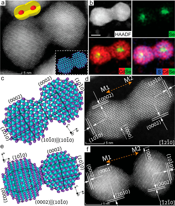
During the masking step (step 3, in the synthetic scheme, Figure 2a), the CQDs become immobilized and only the top hemisphere sites remain available for the further chemical functionalization. While strong tetrathiol cross-linker molecules and successively the second CQDs are anchored to create linked dimers, the attachment is dictated by the facets bound with the cross-linker, which limits rearrangement of the CQDs in the fusion step, unlike the typical oriented attachment. Thus, a constrained attachment with limited rotational freedom fuses the facets quite strongly but generates dimer structures with both homonymous and heteronymous plane orientations (Figure 2b). High angle annular dark field (HAADF) scanning transmission electron microscopy (STEM) provides precise information about the important parameters governing electronic coupling such as core location, center-to-center distance, and interface integration in the fused CQDs molecules.
HAADF-STEM measurements (Figure 4), reveal a continuous lattice between two adjacent CQDs upon fusion forming the structurally coupled CQDs molecules (Figure 4a). HAADF-EDS elemental mapping clearly shows the fusion of the shell while keeping the cores intact (Figure 4b). Continuous distribution of cadmium (both in core and shell) and sulfur (only in shell) are identified along the dimer axis. Along the same line, selective regions of the selenium (only in core) are clearly identified signifying the cores locations.
Figure 4.
Structural and chemical mapping of CQD molecules. HAADF-STEM image (a) and HAADF-EDS elemental mapping (b) of the coupled CdSe/CdS molecules. Atomic structure model and HAADF-STEM image, respectively, for (c,d) homoplane attachment and (e,f) heteroplane attachment in fused dimers. For homoplane attachment, the identical (101̅0) faces of M1 and M2 remain parallel, while for the heteroplane attachment the parallel crystallographic faces are different [(0002) and (101̅0)], as observed under the same zone axis of [1̅21̅0]. Adapted from ref (1), Copyright 2019 Springer Nature.
The constrained attachment results in the homoplane and heteroplane fusion relationships as observed by the HAADF-STEM (Figure 4c–f), well-correlated with the simulated atomic structure model. As the specific facets of the wurtzite CdSe/CdS QDs possess (0002), (101̅0), and (101̅1) planes, several attachment scenarios emerge during the formation of the coupled CQDs molecules, unlike the typical OA process. In homoplane attachment cases, both CQD monomers of a fused pair are projected under the same zone axis without any dislocation along the interface, leading to a high fusion area. This facilitate stronger tunnel coupling strength than in a dimer with low fusion area expected in the heteroplane attachment cases.
5. Hybridization and Electronic Coupling Effects in Homodimer CQD Molecules
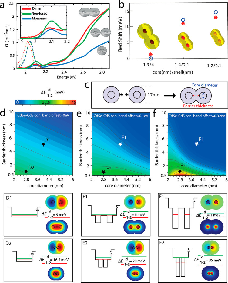
While the attachment of two monomers to form a cross-linked dimer does not change band-edge transitions, the fusion step alters significantly both the absorption and emission features (Figure 5a).2 Upon fusion, the only barrier which remains is the CdS shell, separating the two cores. However, when the barrier is thick and the cores are larger like in the case of 1.9 nm/4 nm core radius/shell thickness, the two electron wave functions on each of the cores remain localized in the big cores and along with the thick barrier in between the cores; this leads to a small red-shift of only 1–2 meV (Figure 5b). As the cores become smaller, the electron wave functions start to delocalize the CdS shell, and along with the thinner barrier thickness the electronic states on each of the cores start to hybridize. This is well manifested in the red-shift of the 1.4/2.1 nm and the 1.2/2.1 nm core-radius/shell–thickness, by 11 and 13 meV, respectively (Figure 5b).1
Figure 5.
(a) Absorption cross section (solid-lines) and normalized emission spectra (dashed-lines) for the monomer (blue), nonfused dimer (green), and fused dimer (red). Adapted from ref (2). Copyright 2019 American Institute of Physics. (b) Calculated (red asterisk) and experimental (blue circles) band-edge red-shift of monomer-to-respective-homodimer structures for different CQD molecules. Adapted from ref (1), Copyright 2019 Springer Nature. (c) The barrier width is controlled by overlapping the two outer spheres of the core/shell CQDs. (d) Contour plot of the energy splitting between the symmetric and antisymmetric states as a function of barrier thickness and core diameter in (d) 0, (e) 0.1, and (f) 0.32 eV CB offsets. The eigen-energies of the symmetric state (red-line) and antisymmetric state (green-line) for the electron with respect to the potential energy landscape along with corresponding wave functions are presented for the points D1-F2 in the contours. Adapted from ref (2). Copyright 2019 American Institute of Physics.
To test the influence of the core diameter and the barrier thickness and to find general design rules for the dimers, we have simulated the dimer structure using Comsol Multi-Physics and solved the electron and hole Schrödinger equations using the effective-mass approximation. The conduction (CB) and valence band (VB) offset between CdSe to CdS, which serve in our system as the barrier height, is under debate in the literature and ranging between 0 eV-0.3 eV for the CB offset, and we show results for 3 representative values: 0 eV, 0.1 and 0.32 eV. In any of the above-mentioned cases, the VB offset is quite large and together with the heavier hole effective-mass, no significant hybridization is expected for the hole. So from now on we will concentrate on the electron energy levels.
The effect of the barrier thickness is highlighted by taking fixed monomers with an overall dimer diameter of 17 nm varying the overlap between them, in addition to tuning core sizes. As expected, for the thicker shell barrier and larger core diameter, the hybridization energy E1–2d, which is the energy difference between the bonding and antibonding states, decreases. In addition, the decrease in the hybridization energy E1–2 is more pronounced in the case of larger band-offset because of the higher barrier height (points D1, E1, and F1 in Figure 5d–f). Interestingly, in the case of a thin barrier and small core diameters the trend is opposite (points D2, E2, and F2 in Figure 5d–f).2
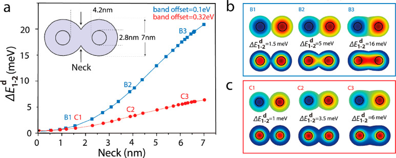
Another crucial parameter which can greatly influence the hybridization energy is the neck formed between the monomers upon fusion (Figure 6a). The overlap diameter was varied between 0 nm, as in nonfused dimer, and 7 nm which resembles a totally fused dimer. A general trend of increasing hybridization energy with filling the neck prevails considering the CB offset values of 0.1 and 0.32 eV. This confirms that, for the mall neck that arises with inefficient fusion, the neck constriction between the monomers acts as a potential barrier, suppressing the hybridization (Figure 6b,c). However, in the case of the 0.32 eV CB offset the change in the hybridization energy is moderate, changing up to 6 meV with complete neck filling, compared to more pronounced change up to ∼20 meV for a 0.1 eV CB-offset (Figure 6a).
Figure 6.
(a) Energy difference between the symmetric and antisymmetric states as a function of the neck diameter for the 0.1 eV (blue) and 0.32 eV (red) CB offset in 1.4/2.1 homodimer. (b,c) Wave functions of the symmetric (bottom) and antisymmetric (top) electronic states and the energy difference between them in three points: which refer to 1.5, 4, and 6.2 nm neck thickness, respectively, for the (b) 0.1 eV band offset (B1–B3) and (c) 0.32 eV band offset (C1–C3). Adapted from ref (2). Copyright 2019 American Institute of Physics.
The difference can be realized from the wave functions of the bonding and antibonding states for the two CB offsets. In the case of the 0.1 eV CB offset, the electron wave function is delocalized in the CdS shell and hence the neck greatly influences the hybridization (B1, B2, and B3 in Figure 6b). However, for the 0.32 eV CB offset, the electron wave function remains localized in the core region and the neck restriction has less influence on the hybridization energy (C1, C2, and C3 in Figure 6c). It should be noted that the hybridization energy is not the only factor which determines the magnitude of monomer-to-dimer red-shift. The electron–hole Coulomb interaction greatly influences the red-shift and we should expect a moderate magnitude considering the Coulomb term.2
6. Coupling Mechanisms in Homodimer CQD Molecules
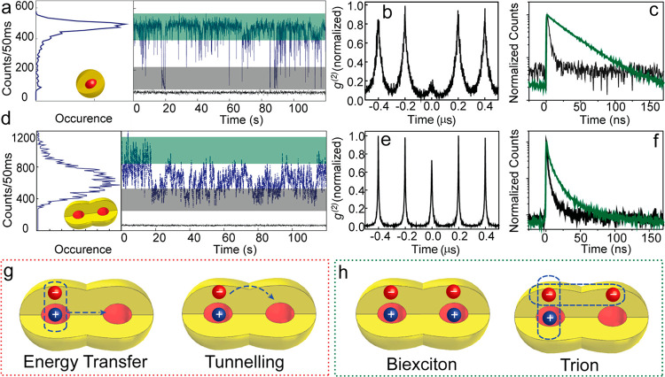
In a homodimer CQD molecule, various coupling mechanisms, on top of the aforementioned hybridization, may become relevant. Resonant dipolar coupling or charge transfer interactions are possible, resulting in novel redistribution of the charge carriers in CQD molecules. Single particle emission studies prove to be a powerful means to address these different possibilities. Individual monomer CQDs undergo the widely studied on-to-off blinking under photoexcitation as a result of exciton pair recombination and three carrier nonradiative Auger recombination, respectively (Figure 7a).46 This phenomena is typically indicated by a long monoexponential radiative decay from the former bright state and a much faster decay from the latter dark state (Figure 7c). At the single exciton regime, the fused CQD molecule rather exhibits a flickering of emission intensity without a clear on or off state (Figure 7d), associated with a faster multiexponential decay (Figure 7f). The quenching of the radiative decay time is observed and may be associated with both charge transfer and fast energy transfer processes between two CQDs, which occur before the successful recombination of the electron and hole within a single CQD. The dipolar fluorescence resonant energy transfer (FRET) remains a contributing factor for the faster decay rate as the organically linked nonfused dimer, where a tunneling of electron through the high barrier is less prominent, also exhibits some quenching (to smaller extent than the fused dimer). The nonradiative off state, obvious in the monomer with the characteristic short lifetime designated to dark trions, was not observed in the studied dimers, as the extracted lifetime from the lowest intensity tags from single dimer remains significantly longer than that in monomers. This indicates the presence of a competitive pathway (viz. tunneling) which restricts fast Auger recombination to occur within one of the dots. Subsequently, owing to larger volume, the dimer can accommodate and stabilize trions efficiently by reducing the Auger rate itself enhancing the lifetime of the charged configuration (Figure 7d,f).
Figure 7.
Photophysical aspects of CQD molecules. Fluorescence time traces (a,d), second order photon correlation (b,e), and luminescence state dependent lifetimes (c,f), respectively, from a single monomer (upper panel) CQD and homodimer CQD molecule (lower panel). (g) Quenching mechanism via interparticle interaction and (h) novel multicarrier configurations in CQD dimer molecule. Adapted from ref (1), Copyright 2019 Springer Nature.
Thus, novel and interesting multicarrier configurations are possible in fused CQD molecules. The nonemissive off or weakly emissive gray states in colloidal CdSe/CdS CQDs arises due to efficient Auger recombination of the photogenerated trion states in thin shell CQDs. Significant reduction in the Auger process was achieved in giant shell CQDs, where the spatial separation between the charge carriers reduces the overlap and slows down the Auger rate.47,48 The CQD molecule can offer new types of multicarrier configurations where the extra electron can tunnel to the second core and thus increase the trion lifetime due to spatial separation as compared to monomers. A biexciton configuration accommodating each exciton pair in either core is an additional interesting feature that can be achieved in CQD molecules. A significant increase in biexciton quantum yield in CQD molecules revealed by the photon correlation statistics is shown in Figure 7e. At low intensity pulsed excitation, a near perfect photon antibunching at the zero time delay is observed in monomers, as the biexciton quantum yield in a thin shell CQD is lower owing to fast Auger decay.49 On the other hand, a reduction in Auger rate enables significant photon bunching in the CQD molecule with a biexciton to exciton quantum yield ratio of up to 0.6 (Figure 7e) compared to monomer CQD revealing the value of <0.1 (Figure 7b).50 The realization of the new biexciton configuration is of importance toward the utilization of CQD molecules in lasing applications.
7. Conclusion and Perspectives
Predesigned and on-demand electronic coupling strength is the key advantage with the coupled artificial molecules formed from core/shell building blocks by wet chemical approaches, that provide numerous opportunities for rational variation of the confined wave functions, along with controlling the extent of hybridization. Tuning the core and shell parameters, i.e., the size, composition, and thickness, can feasibly create a wide variety of heterostructured artificial molecules, with potential toward diverse emerging applications (Figure 8).
Figure 8.
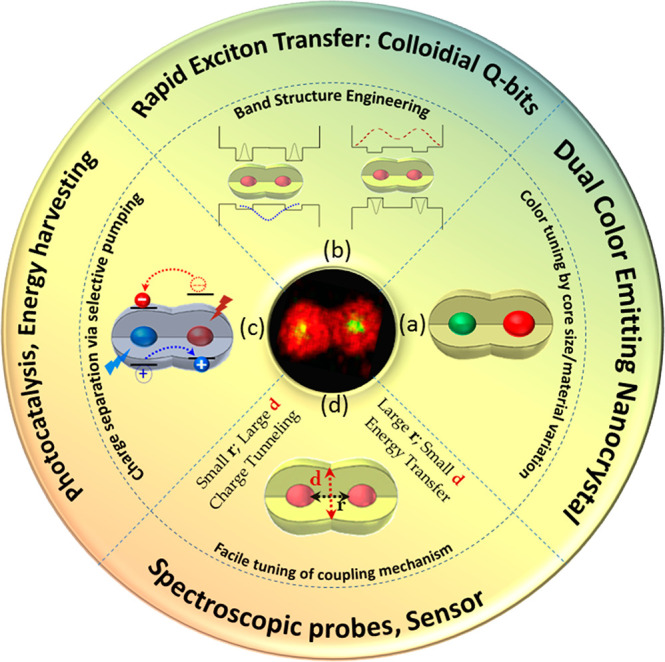
Library for rational design of parameters in fused core/shell dimer molecules toward potential applications. Systematic variation in the monomer units alters the extent and mode of coupling accordingly to achieve specific functionalities.
(a) In a fused dimer molecule, the core size variation can manifest dual color emission from a single quantum system. The ability to tune and switch the emission color conforming to display applications is achievable in the CQD molecules by tailoring the core size and composition without changing the synthetic procedure.
(b) In type-II core/shell CQDs, the staggered band alignment allows extensive delocalization of the one type of carrier to the shell. A higher degree of delocalization can facilitate the transfer of charge carriers to the neighboring CQDs. With a dictated barrier, a systematic alteration of rapid charge carrier transfer is relevant to the quantum information application where the coupled CQDs may serve as Q-bits. This relies on the superposition of the charge carrier states, coulomb-interaction and coherent tunneling, those remain interesting topics of study for the near future in single dimer, a system which exhibit coupling energy resolvable at room temperature (>10 meV)
(c) Through band-structure engineering, a long-lived charge carrier that is of relevance for light harvesting applications can rationally be designed and achieved in a CQD molecule with staggered band alignment of the two cores. The electron and hole wave functions, being in two different dots reduces the overlap between them, would make the charge carriers longer lived.
(d) The systematic change in the barrier, simply by changing the shell thickness, i.e., yardstick for the center-to-center separation, brands the fused CQD molecules as ideal candidates to probe the coupling mechanism and underlying photophysics. At larger separation of the cores, resonance energy transfer dominates the photophysical process, while at shorter distance charge tunneling prevails. The inherent electric field and the external perturbation of the same rely greatly on the degree and mode of coupling, where the photogenerated exciton can tunnel and switch between dots with modulation of e-field fostering CQD molecules for the utilization as electric field sensors.
Apart from the directions and applications discussed, the hybridization of different atomic states such as the s and p states from different dots with comparable energy can also be hybridized which truly can construct the library of hybrid artificial molecules. In these systems, the coupling attributes in the coupled colloidal nanostructures including fused homodimer molecule and other particular heterostructures may be revealed at ambient conditions.
Feasible and targeted synthesis of colloidal nanocrystals with desired dimensionality and functionality has enriched nanoscience during the last decades. Complex architectures with hybrid optical and electrical properties manifest a contemporary and rapidly developing research field. In this Account, we have demonstrated how rational adjunction of nanocrystal artificial atoms offers the flexibility to control the hybridization of individual quantum states. All these rely on the ultimate level of understanding the complex interaction in the individual systems, manifesting a bright future for colloidal quantum dot molecules.
Acknowledgments
The research leading to these results has received financial support from the European Research Council (ERC) under the European Union’s Horizon 2020 research and innovation programme (grant agreement No [741767]). J.B.C and S.K acknowledge the support from the Planning and Budgeting Committee of the higher board of education in Israel through a fellowship. U.B. thanks the Alfred & Erica Larisch memorial chair. Y.E.P. acknowledges support by the Ministry of Science and Technology & the National Foundation for Applied and Engineering Sciences, Israel.
Biographies
Somnath Koley received his M.Sc. in chemistry from Indian School of Mines and PhD from National Institute of Science Education and Research, India. He joined Prof. Banin’s group as a postdoctoral researcher in November 2017. His research interest focuses on the study of optoelectronic properties of single semiconductor nanocrystals and their assemblies using spectroscopic techniques.
Jiabin Cui received his PhD in Beijing University of Chemical Technology under the guidance of Prof. Leyu Wang. He works with Prof. Uri Banin as a postdoctoral fellow at the Hebrew University of Jerusalem in Israel from 2017. His research focuses on the synthesis of coupled nanocrystal molecules, fluorescent nanoprobes, and developing new applications based on the sensor, photothermal therapy, and molecular imaging.
Yossef E. Panfil completed his BSc at JCT and then his MSc in Applied Physics at the Hebrew University of Jerusalem. He is currently a PhD student at the Hebrew University of Jerusalem in Prof. Banin’s group. His research focuses on coupling effects in coupled colloidal Semiconductor QD molecules, using a combination of novel single nanocrystal spectroscopy methods and numerical computations.
Uri Banin holds the Alfred & Erica Larisch Memorial Chair at the Institute of Chemistry and the Center for Nanoscience and Nanotechnology at the Hebrew University of Jerusalem (HU). He was the founding director of the HU Center for Nanoscience and Nanotechnology (2001–2010) and is a founder of Qlight Nanotech, which was acquired by Merck KGaA, Darmstadt, Germany. His research focuses on chemistry and physics of nanocrystals including synthesis of nanoparticles, size- and shape-dependent properties, and emerging applications in displays, lighting, solar energy harvesting, 3D printing, electronics, and biology.
Author Contributions
§ S.K., J.C., and Y.E.P. contributed equally to this work.
The authors declare no competing financial interest.
Special Issue
Published as part of the Accounts of Chemical Research special issue “Transformative Inorganic Nanocrystals”.
References
- Cui J.; Panfil Y. E.; Koley S.; Shamalia D.; Waiskopf N.; Remennik S.; Popov I.; Oded M.; Banin U. Colloidal Quantum Dot Molecules Manifesting Quantum Coupling at Room Temperature. Nat. Commun. 2019, 10 (1), 5401. 10.1038/s41467-019-13349-1. [DOI] [PMC free article] [PubMed] [Google Scholar]
- Panfil Y. E.; Shamalia D.; Cui J.; Koley S.; Banin U. Electronic Coupling in Colloidal Quantum Dot Molecules; the Case of CdSe/CdS Core/Shell Homodimers. J. Chem. Phys. 2019, 151 (22), 224501. 10.1063/1.5128086. [DOI] [PubMed] [Google Scholar]
- Jia G.; Sitt A.; Hitin G. B.; Hadar I.; Bekenstein Y.; Amit Y.; Popov I.; Banin U. Couples of Colloidal Semiconductor Nanorods Formed by Self-Limited Assembly. Nat. Mater. 2014, 13 (3), 301–307. 10.1038/nmat3867. [DOI] [PubMed] [Google Scholar]
- Alivisatos A. P. Semiconductor Clusters, Nanocrystals, and Quantum Dots. Science 1996, 271 (5251), 933–937. 10.1126/science.271.5251.933. [DOI] [Google Scholar]
- Kagan C. R.; Lifshitz E.; Sargent E. H.; Talapin D. V. Building Devices from Colloidal Quantum Dots. Science 2016, 353 (6302), aac5523. 10.1126/science.aac5523. [DOI] [PubMed] [Google Scholar]
- Brus L. E. Electronic Structure and Photoexcited Carrier Dynamics in Nanometer Size CdSe Clusters. J. Chem. Phys. 1984, 80 (9), 4403–4409. 10.1063/1.447218. [DOI] [PubMed] [Google Scholar]
- Bawendi M. G.; Wilson W. L.; Rothberg L.; Carroll P. J.; Jedju T. M.; Steigerwald M. L.; Brus L. E. Electron–Electron and Electron Hole Interactions in Small Semiconductor Crystallites: The Size Dependence of the Lowest Excited Electronic State. Phys. Rev. Lett. 1990, 65 (13), 1623–1626. 10.1103/PhysRevLett.65.1623. [DOI] [PubMed] [Google Scholar]
- Ekimov A. I.; Efros A. L.; Onushchenko A. A. Quantum Size Effect in Semiconductor Microcrystals. Solid State Commun. 1985, 56 (11), 921–924. 10.1016/S0038-1098(85)80025-9. [DOI] [Google Scholar]
- Panfil Y. E.; Oded M.; Banin U. Colloidal Quantum Nanostructures: Emerging Materials for Display Applications. Angew. Chem., Int. Ed. 2018, 57 (16), 4274–4295. 10.1002/anie.201708510. [DOI] [PMC free article] [PubMed] [Google Scholar]
- Kouwenhoven L. Coupled Quantum Dots As Artificial Molecules. Science 1995, 268 (5216), 1440–1441. 10.1126/science.268.5216.1440. [DOI] [PubMed] [Google Scholar]
- Schedelbeck G.; Wegscheider W.; Bichler M.; Abstreiter G. Coupled Quantum Dots Fabricated by Cleaved Edge Overgrowth: From Artificial Atoms to Molecules. Science 1997, 278 (5344), 1792–1795. 10.1126/science.278.5344.1792. [DOI] [PubMed] [Google Scholar]
- Banin U.; Cao Y.; Katz D.; Millo O. Identification of Atomic-like Electronic States in Indium Arsenide Nanocrystal Quantum Dots. Nature 1999, 400 (6744), 542–544. 10.1038/22979. [DOI] [Google Scholar]
- Coden M.; De Checchi P.; Fresch B. Spectral Shift, Electronic Coupling and Exciton Delocalization in Nanocrystal Dimers: Insights from All-Atom Electronic Structure Computations. Nanoscale 2020, 12 (35), 18124–18136. 10.1039/D0NR05601D. [DOI] [PubMed] [Google Scholar]
- Millo O.; Katz D.; Cao Y. W.; Banin U. Imaging and Spectroscopy of Artificial-Atom States in Core/Shell Nanocrystal Quantum Dots. Phys. Rev. Lett. 2001, 86 (25), 5751–5754. 10.1103/PhysRevLett.86.5751. [DOI] [PubMed] [Google Scholar]
- Rodary G.; Bernardi L.; David C.; Fain B.; Lemaître A.; Girard J.-C. Real Space Observation of Electronic Coupling between Self-Assembled Quantum Dots. Nano Lett. 2019, 19 (6), 3699–3706. 10.1021/acs.nanolett.9b00772. [DOI] [PubMed] [Google Scholar]
- Świderski M.; Zieliński M. Electric Field Tuning of Excitonic Fine-Structure Splitting in Asymmetric InAs/InP Nanowire Quantum Dot Molecules. Phys. Rev. B: Condens. Matter Mater. Phys. 2019, 100 (23), 235417. 10.1103/PhysRevB.100.235417. [DOI] [Google Scholar]
- Bayer M.; Hawrylak P.; Hinzer K.; Fafard S.; Korkusinski M.; Wasilewski Z. R.; Stern O.; Forchel A. Coupling and Entangling of Quantum States in Quantum Dot Molecules. Science 2001, 291 (19), 451–453. 10.1126/science.291.5503.451. [DOI] [PubMed] [Google Scholar]
- Stinaff E. A.; Scheibner M.; Bracker A. S.; Ponomarev I. V.; Korenev V. L.; Ware M. E.; Doty M. F.; Reinecke T. L.; Gammon D. Optical Signatures of Coupled Quantum Dots. Science 2006, 311 (5761), 636–639. 10.1126/science.1121189. [DOI] [PubMed] [Google Scholar]
- Mews A.; Eychmueller A.; Giersig M.; Schooss D.; Weller H. Preparation, Characterization, and Photophysics of the Quantum Dot Quantum Well System Cadmium Sulfide/Mercury Sulfide/Cadmium Sulfide. J. Phys. Chem. 1994, 98 (3), 934–941. 10.1021/j100054a032. [DOI] [Google Scholar]
- Battaglia D.; Blackman B.; Peng X. G. Coupled and Decoupled Dual Quantum Systems in One Semiconductor Nanocrystal. J. Am. Chem. Soc. 2005, 127 (31), 10889–10897. 10.1021/ja0437297. [DOI] [PubMed] [Google Scholar]
- Deutsch Z.; Neeman L.; Oron D. Luminescence Upconversion in Colloidal Double Quantum Dots. Nat. Nanotechnol. 2013, 8 (9), 649–653. 10.1038/nnano.2013.146. [DOI] [PubMed] [Google Scholar]
- Teitelboim A.; Meir N.; Kazes M.; Oron D. Colloidal Double Quantum Dots. Acc. Chem. Res. 2016, 49 (5), 902–910. 10.1021/acs.accounts.5b00554. [DOI] [PMC free article] [PubMed] [Google Scholar]
- Oh N.; Kim B. H.; Cho S.-Y.; Nam S.; Rogers S. P.; Jiang Y.; Flanagan J. C.; Zhai Y.; Kim J.-H.; Lee J.; et al. Double-Heterojunction Nanorod Light-Responsive LEDs for Display Applications. Science 2017, 355 (6325), 616–619. 10.1126/science.aal2038. [DOI] [PubMed] [Google Scholar]
- Nikolic M. S.; Olsson C.; Salcher A.; Kornowski A.; Rank A.; Schubert R.; Froemsdorf A.; Weller H.; Foerster S. Micelle and Vesicle Formation of Amphiphilic Nanoparticles. Angew. Chem., Int. Ed. 2009, 48 (15), 2752–2754. 10.1002/anie.200805158. [DOI] [PubMed] [Google Scholar]
- Alivisatos A. P.; Johnsson K. P.; Peng X.; Wilson T. E.; Loweth C. J.; Bruchez M. P.; Schultz P. G. Organization of “nanocrystal Molecules” Using DNA. Nature 1996, 382 (6592), 609–611. 10.1038/382609a0. [DOI] [PubMed] [Google Scholar]
- Graff B. M.; Bloom B. P.; Wierzbinski E.; Waldeck D. H. Electron Transfer in Nanoparticle Dyads Assembled on a Colloidal Template. J. Am. Chem. Soc. 2016, 138 (40), 13260–13270. 10.1021/jacs.6b06991. [DOI] [PubMed] [Google Scholar]
- Lu C.; Tang Z. Advanced Inorganic Nanoarchitectures from Oriented Self-Assembly. Adv. Mater. 2016, 28 (6), 1096–1108. 10.1002/adma.201502869. [DOI] [PubMed] [Google Scholar]
- Tang Z. Y.; Kotov N. A. One-Dimensional Assemblies of Nanoparticles: Preparation, Properties, and Promise. Adv. Mater. 2005, 17 (8), 951–962. 10.1002/adma.200401593. [DOI] [Google Scholar]
- Zhang H.; Hu B.; Sun L.; Hovden R.; Wise F. W.; Muller D. A.; Robinson R. D. Surfactant Ligand Removal and Rational Fabrication of Inorganically Connected Quantum Dots. Nano Lett. 2011, 11 (12), 5356–5361. 10.1021/nl202892p. [DOI] [PubMed] [Google Scholar]
- Liu J.; Guillemeney L.; Abécassis B.; Coolen L. Long Range Energy Transfer in Self-Assembled Stacks of Semiconducting Nanoplatelets. Nano Lett. 2020, 20 (5), 3465–3470. 10.1021/acs.nanolett.0c00376. [DOI] [PubMed] [Google Scholar]
- Collini E.; Gattuso H.; Kolodny Y.; Bolzonello L.; Volpato A.; Fridman H. T.; Yochelis S.; Mor M.; Dehnel J.; Lifshitz E.; et al. Room-Temperature Inter-Dot Coherent Dynamics in Multilayer Quantum Dot Materials. J. Phys. Chem. C 2020, 124 (29), 16222–16231. 10.1021/acs.jpcc.0c05572. [DOI] [Google Scholar]
- Gilmore R. H.; Liu Y.; Shcherbakov-Wu W.; Dahod N. S.; Lee E. M. Y.; Weidman M. C.; Li H.; Jean J.; Bulović V.; Willard A. P.; et al. Epitaxial Dimers and Auger-Assisted Detrapping in PbS Quantum Dot Solids. Matter 2019, 1 (1), 250–265. 10.1016/j.matt.2019.05.015. [DOI] [Google Scholar]
- Dibenedetto C. N.; Fanizza E.; Brescia R.; Kolodny Y.; Remennik S.; Panniello A.; Depalo N.; Yochelis S.; Comparelli R.; Agostiano A.; et al. Coupling Effects in QD Dimers at Sub-Nanometer Interparticle Distance. Nano Res. 2020, 13 (4), 1071–1080. 10.1007/s12274-020-2747-3. [DOI] [Google Scholar]
- Penn R. L.; Banfield J. F. Imperfect Oriented Attachment: Dislocation Generation in Defect-Free Nanocrystals. Science. 1998, 281 (5379), 969–971. 10.1126/science.281.5379.969. [DOI] [PubMed] [Google Scholar]
- Cho K. S.; Talapin D. V.; Gaschler W.; Murray C. B. Designing PbSe Nanowires and Nanorings through Oriented Attachment of Nanoparticles. J. Am. Chem. Soc. 2005, 127 (19), 7140–7147. 10.1021/ja050107s. [DOI] [PubMed] [Google Scholar]
- Schliehe C.; Juarez B. H.; Pelletier M.; Jander S.; Greshnykh D.; Nagel M.; Meyer A.; Foerster S.; Kornowski A.; Klinke C.; et al. Ultrathin PbS Sheets by Two-Dimensional Oriented Attachment. Science 2010, 329 (30), 550–554. 10.1126/science.1188035. [DOI] [PubMed] [Google Scholar]
- Boneschanscher M. P.; Evers W. H.; Geuchies J. J.; Altantzis T.; Goris B.; Rabouw F. T.; van Rossum S. A. P.; van der Zant H. S. J.; Siebbeles L. D. A.; Van Tendeloo G.; et al. Long-Range Orientation and Atomic Attachment of Nanocrystals in 2D Honeycomb Superlattices. Science 2014, 344 (6190), 1377–1380. 10.1126/science.1252642. [DOI] [PubMed] [Google Scholar]
- Fang L.; Wang Y.; Liu M.; Gong M.; Xu A.; Deng Z. Dry Sintering Meets Wet Silver-Ion “Soldering”: Charge-Transfer Plasmon Engineering of Solution-Assembled Gold Nanodimers From Visible to Near-Infrared I and II Regions. Angew. Chem., Int. Ed. 2016, 55 (46), 14296. 10.1002/anie.201608271. [DOI] [PubMed] [Google Scholar]
- Li B.; Bian K.; Zhou X.; Lu P.; Liu S.; Brener I.; Sinclair M.; Luk T.; Schunk H.; Alarid L.; et al. Pressure Compression of CdSe Nanoparticles into Luminescent Nanowires. Sci. Adv. 2017, 3 (5), e1602916. 10.1126/sciadv.1602916. [DOI] [PMC free article] [PubMed] [Google Scholar]
- Luo D.; Yan C.; Wang T. Interparticle Forces Underlying Nanoparticle Self-Assemblies. Small 2015, 11 (45), 5984–6008. 10.1002/smll.201501783. [DOI] [PubMed] [Google Scholar]
- Hughes B. K.; Blackburn J. L.; Kroupa D.; Shabaev A.; Erwin S. C.; Efros A. L.; Nozik A. J.; Luther J. M.; Beard M. C. Synthesis and Spectroscopy of Pbse Fused Quantum-Dot Dimers. J. Am. Chem. Soc. 2014, 136 (12), 4670–4679. 10.1021/ja413026h. [DOI] [PubMed] [Google Scholar]
- Ondry J. C.; Hauwiller M. R.; Alivisatos A. P. Dynamics and Removal Pathway of Edge Dislocations in Imperfectly Attached PbTe Nanocrystal Pairs: Toward Design Rules for Oriented Attachment. ACS Nano 2018, 12 (4), 3178–3189. 10.1021/acsnano.8b00638. [DOI] [PubMed] [Google Scholar]
- Ondry J. C.; Philbin J. P.; Lostica M.; Rabani E.; Alivisatos A. P. Resilient Pathways to Atomic Attachment of Quantum Dot Dimers and Artificial Solids from Faceted CdSe Quantum Dot Building Blocks. ACS Nano 2019, 13 (11), 12322–12344. 10.1021/acsnano.9b03052. [DOI] [PubMed] [Google Scholar]
- Hu Y.; Sun Y. A Generic Approach for the Synthesis of Dimer Nanoclusters and Asymmetric Nanoassemblies. J. Am. Chem. Soc. 2013, 135 (6), 2213–2221. 10.1021/ja309501s. [DOI] [PubMed] [Google Scholar]
- Qiu J.; Xie M.; Lyu Z.; Gilroy K. D.; Liu H.; Xia Y. General Approach to the Synthesis of Heterodimers of Metal Nanoparticles through Site-Selected Protection and Growth. Nano Lett. 2019, 19 (9), 6703–6708. 10.1021/acs.nanolett.9b03167. [DOI] [PubMed] [Google Scholar]
- Galland C.; Ghosh Y.; Steinbrueck A.; Sykora M.; Hollingsworth J. A.; Klimov V. I.; Htoon H. Two Types of Luminescence Blinking Revealed by Spectroelectrochemistry of Single Quantum Dots. Nature 2011, 479 (7372), 203–207. 10.1038/nature10569. [DOI] [PMC free article] [PubMed] [Google Scholar]
- Park Y.-S.; Bae W. K.; Pietryga J. M.; Klimov V. I. Auger Recombination of Biexcitons and Negative and Positive Trions in Individual Quantum Dots. ACS Nano 2014, 8 (7), 7288–7296. 10.1021/nn5023473. [DOI] [PubMed] [Google Scholar]
- Wu K.; Lim J.; Klimov V. I. Superposition Principle in Auger Recombination of Charged and Neutral Multicarrier States in Semiconductor Quantum Dots. ACS Nano 2017, 11 (8), 8437–8447. 10.1021/acsnano.7b04079. [DOI] [PubMed] [Google Scholar]
- Park Y.-S.; Malko A. V.; Vela J.; Chen Y.; Ghosh Y.; García-Santamaría F.; Hollingsworth J. A.; Klimov V. I.; Htoon H. Near-Unity Quantum Yields of Biexciton Emission from CdSe/CdS Nanocrystals Measured Using Single-Particle Spectroscopy. Phys. Rev. Lett. 2011, 106 (18), 187401. 10.1103/PhysRevLett.106.187401. [DOI] [PubMed] [Google Scholar]
- Nair G.; Zhao J.; Bawendi M. G. Biexciton Quantum Yield of Single Semiconductor Nanocrystals from Photon Statistics. Nano Lett. 2011, 11 (3), 1136–1140. 10.1021/nl104054t. [DOI] [PMC free article] [PubMed] [Google Scholar]


