

Abstract

Topology, a mathematical concept, has recently become a popular and truly transdisciplinary topic encompassing condensed matter physics, solid state chemistry, and materials science. Since there is a direct connection between real space, namely atoms, valence electrons, bonds, and orbitals, and reciprocal space, namely bands and Fermi surfaces, via symmetry and topology, classifying topological materials within a single-particle picture is possible. Currently, most materials are classified as trivial insulators, semimetals, and metals or as topological insulators, Dirac and Weyl nodal-line semimetals, and topological metals. The key ingredients for topology are certain symmetries, the inert pair effect of the outer electrons leading to inversion of the conduction and valence bands, and spin–orbit coupling. This review presents the topological concepts related to solids from the viewpoint of a solid-state chemist, summarizes techniques for growing single crystals, and describes basic physical property measurement techniques to characterize topological materials beyond their structure and provide examples of such materials. Finally, a brief outlook on the impact of topology in other areas of chemistry is provided at the end of the article.
1. Introduction
We use a variety of synthetic and natural solid materials in our daily lives. Recently, solids have been reclassified through the lens of topology, which goes far beyond the simple sum of their symmetry elements. All known inorganic compounds have been categorized using a single electron approach to trivial and topological materials1−4 and published on the Web.5,6 All scientists can now search for new topological compounds on these Web pages. This new viewpoint has led to the discovery of many unexpected properties, that include large responses to external stimuli, such as field (electric and magnetic), to waves (from light to acoustic waves), and to temperature, pressure, strain, etc. (Figure 1).7−12 So far, we believe that this is only the tip of the iceberg. To date, physicists have mostly contributed to the successful story of topology. A number of solid-state chemists, particularly those who have been influenced by the works of Roald Hoffman,13,14 have joined the topological community.15−18 Now is the time for topology to consider new avenues beyond those of condensed matter physics for example, for catalysis, and solar cells and beyond.
Figure 1.

Typical external stimuli available for manipulating electronic properties of quantum materials. The single crystal at the center of the scheme is of Weyl semimetal TaAs.
Another important and perhaps surprising outcome of research on topology in condensed matter physics is the prediction and realization of table-top experiments for high-energy physics and astrophysics.9 So-called quasiparticles (electrons, holes, phonons, etc.) in topological materials can mimic high energy particles such as the axion19,20 or Majorana particle21−24 or fields in the universe.9
Topology can have impact in many areas of materials research and solid-state chemistry. In compounds such as Dirac semimetals (graphene being the first example), and Weyl semimetals, giant mobilities,8,25 small thermal and hydrodynamic electric conductivities,26 large chiral photocurrents,10 giant magnetoresistance,7,8 and Nernst effects27,28 have been observed, with strong violation of “classical laws” such as the Wiedemann–Franz law,26 a law which limits the figure of merit of thermoelectric materials.29 In magnetic Weyl semimetals large anomalous Hall,30−37 anomalous Nernst,38−40 and magneto optic effects41 have been predicted or measured recently. Redox catalysis may also profit from topological properties42 such as topological protected surface states,43−45 chiral surface states,46 and giant electron mobilities,47,48 despite insulating and semiconducting bulk electronic structures. In the second part of our review, we discuss several examples of giant responses in greater detail to stimulate further research by chemistry groups.
The basic ingredients needed for most topological effects are relativistic effects, and therefore, it is not surprising that in many compounds heavy elements are important building blocks. Relativity contributes in two ways to topological materials, via the inert pair effect and via spin–orbit coupling (SOC). The inert pair effect is responsible for lowering the energy of the outer s electrons 5s and 6s due to the nearly relativistic speed of the 1s electrons in heavy elements such as gold49 and bismuth.16 Many of the heavy p-block elements, such as bismuth, consequently have a different electron configuration in compounds compared to their lighter relatives. In ionic compounds such as Bi2Se3, Bismuth is Bi3+, while phosphorus in H3PO4 is P5+. In classical semiconductors such as silicon, GaAs, etc., the HOMO (highest occupied molecular orbital) or, in the language of physics, the valence band is of p-character and the LUMO (lowest unoccupied molecular orbital) or conduction band is of s-character. A consequence in heavy element semiconductors, such as HgTe50,51 or YPtBi,52 is that the lowest lying conduction band with s character overlaps with the highest lying valence band, see Figure 2a. However, from Hoffmann we have learned that crossing of bands are forbidden depending on their symmetry, and since spin is not a good quantum number many of the crossing points in topological materials will open up and new band gaps will appear with a band inversion (Figure 2a). The symbol for denoting normal or so-called trivial semiconductor is a donut while that for denoting inverted semiconductors is a Möbius stripe (Figure 2b). Since this effect appears in many elements it is not surprising that more than 20% of all inorganic compounds are topological.2−4
Figure 2.

(a) Consequence of inert pair effect observed as band inversion in heavy-element semiconductors. (b) Trivial semiconductors are represented as a donut while the inverted semiconductor is a Möbius strip. A smooth transition is not possible between these two states.
2. Topological and Trivial States of Matter
2.1. Bands in Insulators, Metals, and Topological Insulators
All solid materials can be broadly divided in two categories: metals, which conduct electricity and insulators, which do not. The best way to distinguish between these states is to examine their valence and conduction bands. If the valence band of a material is completely filled and separated from the conduction band by an energy gap, then it can be considered an insulator or a semiconductor (Figure 3). In an insulator such as diamond, the energy gap between the valence and conduction bands, known as the band gap, is so large that, at any practical temperature, electrons cannot be excited from the valence band to the conduction band. By contrast, semiconductors such as silicon and germanium have small band gaps such that thermal excitations at high temperatures cause some electrons from the top of the valence band to populate the bottom of the conduction band. Therefore, at absolute zero temperature, because of zero thermal excitations, a semiconductor behaves as an insulator. However, in metals, the valence and conduction bands overlap with each other, and hence, the band gap is not defined. This overlap ensures that electrons are always available for conduction at absolute zero and at all finite temperatures. Furthermore, topological insulators constitute a new class of exotic materials that can neither be classified as pure insulators/semiconductors nor as metals. Inside the material or in the bulk, the valence and conduction bands are separated by the band gap, whereas on the surface, the valence and conduction bands are connected by metallic states also known as topological surface states.53−57 Surface bands cross linearly to form graphene-like Dirac cones at the surface. One of the most important features of this surface state is that the spin and the momentum of the electrons are locked perpendicular to each other due to SOC. Hence, electrons carrying opposite spins propagate in opposite directions (see Figure 4b). This prevents the backscattering of electrons at the surface of a topological insulator because it requires the electron to flip its spin. Kane and Mele presented the first prototypical example of a two-dimensional topological insulating phase in graphene.58 Owing to the very small SOC of the carbon atom, the band gap is so small that it is not possible to access the dissipationless edge currents in graphene experimentally at any practically low temperature.59,60 Subsequent studies focused on developing systems containing heavy elements such as Bi1–xSbx and strained α-Sn.61,62 Groups led by Cava and Hasan provided the first experimental evidence of Dirac-like surface states on the surface of Bi0.9Sb0.1, a three-dimensional topological insulator, using angle-resolved photoemission spectroscopy (ARPES).63,64 Another approach is to go from elements to compounds. HgTe is a binary semiconductor with heavy elements. The prediction by Bernevig et al.50 for the observation of topological edge states was realized one year later by Molenkamp’s group.51 Afterward, topological surface states were also found in layered tetradymite compounds such as Bi2Se3,65,66 Bi2Te3,67 Sb2Te368 and Bi2Te2Se69,70 (see Figure 4). Many half-Heusler compounds having the general formula XYZ (X,Y are transition metals, where X is more electropositive than Y and Z is a main group element) are potential candidates for the realization of tunable topological insulators.52,71,72 In fact, Liu et al. demonstrated the existence of topological surface states in the superconducting half-Heusler compounds, namely YPtBi and LuPtBi.73 Owing to the excellent tunability of their structures and electronic properties through simple electron counting rules and suitability of thin film growth, Heusler compounds are critical materials for identifying new topological insulators.74 Many more topological insulators have been discovered in inorganic solids, yet plenty of opportunities remain.2−4
Figure 3.
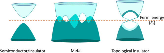
Schematics of electronic bands in various solid state materials. In semiconductors/insulators, the valence and conduction bands are separated by an energy gap. In metals, the valence and conduction bands overlap each other. In topological insulators, after band inversion, the valence and conduction bands are separated by the band gap, leaving behind conducting topological surface states in the form of linearly crossing Dirac cone.
Figure 4.

(a) Crystal structure of the three dimenmsional topological insulator Bi2Te2Se containing quintuple layer units of Te–Bi–Se–Bi–Te. Te and Se atoms occupy separate layers due to their electronegativity difference. (b) ARPES results of Ca-doped Bi2Se3 showing surface Dirac cone below the Fermi energy. At the Fermi energy, the surface states coexist with the conduction band. Upward and downward arrows depict spin-momentum locking of the surface states. Reprinted with permission from ref (65). Copyright 2009 Springer Nature.
In three-dimensional topological insulators all the crystal facets exhibit topological surface states and the number of surface Dirac cones is odd. However, some systems can support such surface states only for some facets while the remaining facets lack topological surface states. Additionally, the total number of band inversions and, therefore, the number of the surface Dirac cones is even. An even number of band crossings is often observed in more layered structures with no dispersion in one direction of the band structure. These systems are known as weak topological insulators.53 The term “weak” was adopted because it was initially believed that the surface states were not robust against crystal disorder, and an energy gap can be created in the Dirac cones by the inclusion of defects. Later, researchers found that the surface states in the weak topological insulators are quite robust against disorder; hence, its name does not fully justify these systems.75 The best way to understand weak topological insulators is to assume a three-dimensional stacking of two-dimensional topological insulators with dissipationless edge states. In this case, the side surfaces will become conducting while the top and bottom surfaces, also known as the dark faces without any topological surface states, will remain insulating. KHgSb is an example of the layered version of HgTe (a two-dimensional topological insulator), predicted as a weak topological insulator in 2012,76 which was later identified to be an hourglass fermion.77 The first experimental weak topological insulator phase was discovered in the hexagonal compound Bi14Rh3I9 wherein the layers with conducting edges can be assumed to stack along the [001].17 This means that the topological surface states will be absent on the surface normal to [001], while all other facets will contain an even number of surface Dirac cones. Other examples of weak topological insulators are β-Bi4I478 and Bi2TeI.79 Interestingly, Bi2TeI, in addition to containing side surface states related to a weak topological insulator, also contains surface states connected to a topological crystalline insulating state which we will discuss next.
In topological insulators the nontrivial metallic surface states are protected by time reversal symmetry. The topological classification of the electronic structure was further extended by using knowledge of the crystal structure and the symmetry of the materials, which led to the discovery of the topological crystalline insulator (TCI).80,81 Unlike topological insulators, here the surface states are protected by the crystal symmetries, such as mirror and rotation. Until now, the TCI phase is experimentally realized in the rock salt structure type (space group Fm3m) SnTe, Pb1–xSnxTe and Pb1–xSnxSe.82−84 For instance, in SnTe the topological surface states are protected by the {110} family of mirror planes and the surface states are only observed on surfaces that are perpendicular to one of the {110} mirror planes. As a consequence, the robust surface states with an even number of Dirac cones can be observed on the crystal facets such as {001}, {110}, or {111}.82,85 Since TCI surface states are protected by the crystal symmetries, it can exhibit a wide range of tunable electronic properties under various perturbations, such as structural distortion/disorder, magnetic dopants, mechanical strain, or thickness engineering.81
2.2. Transport Signatures of Insulators, Metals, and Topological Insulators
As the availability of electrons
for conduction relies on the thermal activation of the electrons from
the valence band, the resistivity of a semiconductor can be well represented
using an Arrhenius equation as  , where ρC is
a material
constant, kB is the Boltzmann constant,
and ΔE is the band gap.86,87 At high temperature, owing to the dominant thermal activation, resistivity
is lower when compared to that at low temperature, where charge carriers
are scarce (Figure 5a). In metals and semimetals, many free electrons are available for
conduction at all temperatures; therefore, the effect of thermal excitation
of electrons on conduction is much less important. Rather, conduction
is affected more by temperature-dependent scattering events, the most
important being the scattering of electrons by lattice vibrations
(phonons). As the scattering of electrons by phonons increases at
high temperature, the resistivity of the material also increases (Figure 5b). A topological
insulator is the combination of a perfect surface conductor and semiconducting
bulk, as reflected by its resistivity. At the high temperature region,
the resistivity increases as the temperature decreases, similar to
that observed in a semiconductor. However, at low temperature, the
resistivity saturates because of the contribution from the conducting
surface states (see Figure 5c). The competition between such two-channel electron transport
mechanisms explains the typical temperature dependent-behavior of
resistivity in topological insulators.88−91
, where ρC is
a material
constant, kB is the Boltzmann constant,
and ΔE is the band gap.86,87 At high temperature, owing to the dominant thermal activation, resistivity
is lower when compared to that at low temperature, where charge carriers
are scarce (Figure 5a). In metals and semimetals, many free electrons are available for
conduction at all temperatures; therefore, the effect of thermal excitation
of electrons on conduction is much less important. Rather, conduction
is affected more by temperature-dependent scattering events, the most
important being the scattering of electrons by lattice vibrations
(phonons). As the scattering of electrons by phonons increases at
high temperature, the resistivity of the material also increases (Figure 5b). A topological
insulator is the combination of a perfect surface conductor and semiconducting
bulk, as reflected by its resistivity. At the high temperature region,
the resistivity increases as the temperature decreases, similar to
that observed in a semiconductor. However, at low temperature, the
resistivity saturates because of the contribution from the conducting
surface states (see Figure 5c). The competition between such two-channel electron transport
mechanisms explains the typical temperature dependent-behavior of
resistivity in topological insulators.88−91
Figure 5.

(a) Schematic representation of charge carrier conduction and typical electrical resistivity as a function of temperature in (a) semiconductors/insulators, (b) metals, and (c) topological insulators. The arrows indicate the charge carrier conduction path.
2.3. Classification of Topological Semimetals
We have seen that two linear bands at the surface of a three-dimensional topological insulator cross the gap between the valence and conduction bands. Therefore, the question that arises is whether such a crossing is also possible in the bulk of metals or semimetals. The answer is “yes”. In fact, the past few years of research have been very fruitful in identifying many Dirac and Weyl semimetals, where such linear crossings of bands occur in the bulk rather than on the surface, as just discussed for the case of topological insulators. As the bulk has three spatial dimensions available, the bands around a Dirac or Weyl crossing point disperse linearly in all three momentum directions with respect to energy.92 As both Dirac and Weyl points result from the linear crossings of bands how do they differ from each other? Crystal structure and magnetism are the main criteria that set them apart. To realize a Weyl semimetal, one must select a system without inversion symmetry. Weyl points in centrosymmetric crystal systems cannot exist unless they also exhibit magnetism, most commonly ferromagnetism; in other words, the system should break time-reversal symmetry. In contrast, Dirac points exist in centrosymmetric crystals without magnetism (see Figure 6a). Because of the coexistence of center of inversion in the crystal structure and the absence of magnetism, all the bands are 2-fold degenerate (Kramers degeneracy) in Dirac systems; that is, they contain both spin-up and spin-down states. Thus, the crossing of two such 2-fold bands at the Dirac point would lead to 4-fold degenerate states as shown in Figure 6e (represented as the crossing of two pairs of lines). In Weyl semimetals, owing to the absence of a center of inversion (see Figure 6b) or due to the presence of magnetism (see Figure 6d), the spin-up and spin-down bands are always separated, except at the high-symmetry points of the Brillouin zone (the Brillouin zone in the momentum world is equivalent to the unit cell of a crystal structure in the real world86). Therefore, the crossing of two nondegenerate bands would result in 2-fold degenerate states at the Weyl points, as shown in Figure 6f (represented as crossing of two lines). From symmetry considerations, the minimum number of Weyl points in a nonmagnetic and magnetic Weyl semimetals are two pairs and one pair, respectively.
Figure 6.

Crystal structure of (a) centrosymmetric hexagonal Dirac semimetal Na3Bi, (b) noncentrosymmetric tetragonal Weyl semimetal TaAs, (c) nonsymmorphic tetragonal Dirac nodal line semimetal ZrSiS, and (d) ferromagnetic kagome lattice Weyl semimetal Co3Sn2S2. Schematic representation of band crossing in (e) Dirac, (f) Weyl, and (g) Nodal line semimetal. In a Dirac semimetal, all bands are doubly degenerate, whereas in a Weyl semimetal, the degeneracy is lifted owing to breaking of the inversion symmetry or the time-reversal symmetry. Positive and negative signs indicate the opposite chirality of the Weyl points. At the surface projection, Weyl points are connected by the surface Fermi arc as depicted by the pink line. The 4-fold and 2-fold degenerate points are shown as crossings of 4 lines in panel e and 2 lines in panel f, respectively. In the case of a nodal line semimetal, the band crossing takes place in a line or a ring, where the topological surface state is two-dimensional in nature, known as the drumhead surface state.
The most important feature of the Weyl points is that they are chiral and occur in pairs of opposite chirality. The chirality of the Weyl points is different from structural chirality; it is possible to obtain chiral Weyl points in achiral crystal structures. For simplicity, Weyl points of the opposite chirality can be considered equivalent to the north and south poles of a magnet in the real world, where the magnetic field lines originate and terminate, respectively. Similarly, the positive and negative chiralities of the Weyl points function as the source and the sink of the commonly known “Berry curvature”, in the momentum world. We will discuss Berry curvature in more detail in section 5. Another important feature of Weyl semimetals is their unique unclosed arc-like topological surface states known as Fermi arcs.93 It is defined as the connecting line between two points on the surface, the two points being the surface projections of Weyl points having opposite chiralities.
It is easy to understand Dirac points in terms of Weyl points. Dirac points are equivalent to the combination of two Weyl points with opposite chiralities; hence, the net chirality of a Dirac point is zero.
However, it is interesting to note that a Dirac point can be split into a pair of Weyl points with opposite chiralities by removing the center of inversion in the crystal, introducing magnetic elements into the crystal to induce ferromagnetism, or applying a high magnetic field. Three-dimensional Dirac states were first discovered in Na3Bi94,95 and Cd3As2,96,97 where the Dirac points are protected by C3 and C4 rotational symmetries, respectively (see Figure 7a). From these discoveries, we can infer that the mere presence of inversion symmetry and nonmagnetic crystal structures does not guarantee Dirac points, and further details of the crystal structures are vital. Furthermore, if we can remove C3 rotational symmetry, as in the case of Na3Bi, it is possible to eliminate Dirac points. This brings us to the next important point regarding the Weyl points, that the “Weyl crossings are accidental crossings”. The term accidental means that Weyl crossings are not necessitated by crystal symmetries and are therefore completely coincident. For this reason, Weyl points are extremely difficult to eliminate, unless one finds a method to manipulate the crystal structure such that Weyl points of opposite chirality come together and annihilate each other. The first candidate compounds for realizing Weyl points were predicted in 2011 in magnetic pyrochlore irridate Y2Ir2O793 and spinel HgCr2Se498 but could not be realized owing to various experimental difficulties. The paradigm shift in Weyl semimetal research had to wait until 2015, when simple nonmagnetic tetragonal noncentrosymmetric semimetallic compounds TaAs, NbAs, TaP, and NbP were predicted to contain several pairs of Weyl points.99 Very soon, owing to the very simple crystal growth techniques needed to grow high quality large single crystals, several research groups experimentally verified the existence of Weyl points using spectroscopic techniques in particular ARPES100−107 (see Figure 7b) and scanning tunneling spectroscopy.104,108 Later, Weyl points were discovered in layered transition metal dichalcogenides, namely WTe2109−112 and MoTe2.113−118 The magnetic counterparts of Weyl semimetals were identified much later in ferromagnetic Heusler compounds.119,120 Experimental verifications of Weyl points were performed in room temperature ferromagnet Co2MnGa121,122 and ferromagnetic shandite Co3Sn2S2.30,31,110,123,124 These findings provide many opportunities for materials scientists to unravel many exotic electrical and thermal transport properties due to the existence of Weyl points. We discuss these properties in detail in the following sections.
Figure 7.

(a) ARPES results of Na3Bi showing Dirac crossing between the conduction and valence band in the bulk below the Fermi energy. BCB and BVB denote the bulk conduction band and the bulk valence band, respectively. Reprinted with permission from ref (95). Copyright 2014 AAAS. (b) (i) A pair of Weyl points in the bulk Brillouin zone in the TaAs family of Weyl semimetals. Panels (ii), (iii), and (iv) show the calculated (left) and experimental surface Fermi arcs in NbP, TaP, and TaAs, respectively. The separation between the Weyl points of opposite chirality, and therefore the length of the Fermi arc increase with increased SOC, i.e., the molecular weight of the compounds. Reprinted with permission from ref (105). Copyright 2016 Springer Nature.
In Dirac and Weyl semimetals, valence and conduction bands cross at a point. However, there can be a more general situation, where the crossing occurs at a line or a ring, protected by certain crystalline symmetries. In such situations, they are called topological nodal-line or a nodal-ring semimetals (see Figure 6g). The generality of the nodal line can be highlighted by the fact that many Weyl and Dirac semimetals originate from nodal lines owing to SOC. Stabilization of such extended states requires additional crystalline symmetries, most commonly a mirror reflection. The degeneracy arising from line-crossing can be 2-fold, such as that in a Weyl semimetal or 4-fold, as observed in a Dirac semimetal. Nodal-ring crossing in PbTaSe2,125 a nonmagnetic superconductor, is 2-fold degenerate because the crystal structure lacks inversion symmetry. The layered hexagonal structure of PbTaSe2 can be described as the Pb-intercalation of TaSe2, a transition metal dichalcogenide, where the Pb-layer acts as a mirror plane. This mirror plane forces the valence and conduction bands to stick together in a ring. Schoop et al. demonstrated that ZrSiS,126 a Si-square-net compound (see Figure 6c) and related compounds127 are also topological nodal line semimetals. As these compounds are nonmagnetic and their tetragonal crystal structures possess inversion symmetry, the nodal-line is 4-fold degenerate. In such cases, nodal-lines are protected by the combination of mirror and translational symmetries (a nonsymmorphic symmetry) of the crystal structures. The position of the nodal-line in ZrSiS is much below the Fermi energy (energy levels up to which the electrons are occupied), and therefore, it is unlikely to influence the transport properties. Topp et al. showed that, owing to the high c/a-ratio of tetragonal structures, it is possible to move the nodal-line near the Fermi energy in ZrSiTe,128 the sister compound of ZrSiS (see Figure 8). Co2MnGa, a Heusler compound, is a ferromagnetic topological nodal-line semimetal,122 where the nodal lines are protected by mirror planes.32,121 Nodal lines are the origin of exotic electrical and thermal transport properties in such compounds. Nodal-ring semimetals contain flat two-dimensional surface states, which are known as drumhead surface states. Drumhead surface state were first observed in topological nodal-line semimetals PbTaSe2125 and TlTaSe2.129 Later, they were also observed in the Weyl fermion line Heusler compound Co2MnGa.122 We discuss these properties in greater detail later.
Figure 8.

Calculated position of the nodal line with respect to the Fermi energy in ZrSiS and related compounds as a function of tetragonal c/a ratio. The nodal line in ZrSiTe resides very close to the Fermi energy. Reprinted from ref (128) with permission under CC BY 3.0 license. Copyright 2016 Deutsche Physikalische Gesellschaft.
3. Single Crystals Growth Techniques
The ability of chemists and materials scientists to grow high-quality single crystals is one of the most important factors influencing the development of topological research. Single crystals are uninterrupted three-dimensional arrays of atoms with repeating geometry present in a single piece of a material. Growing single crystals requires considerable time and effort, as justified by their importance over their polycrystalline counterparts. Single crystals are necessary for determining the intrinsic physical properties without the influence of grain boundaries and impurity phases. They also enable observations of any anisotropic physical properties along various crystallographic axes resulting from anisotropies in the crystal structure. These advantages make single crystals particularly essential for characterizing topological materials through various transport and spectroscopic techniques. Among the many crystal growth techniques available to chemists and materials scientists, the metal-flux, chemical vapor transport (CVT), Bridgman, optical floating zone (OFZ), and Czochralski methods are popular and extremely useful to grow single crystals of a variety of topological materials (see Figure 9). The technique to be applied depends on many factors such as the volatility, thermodynamic stability, extent of doping and size of the final crystal. In the following subsections, we discuss the advantages and disadvantages of these important techniques for growing single crystals of topological materials.
Figure 9.

Schematic showing different single crystals growth techniques.
3.1. Metal Flux Method
Sufficient diffusion of atoms for the successful growth of single crystals generally requires a considerably high temperature. A metal flux that can dissolve constituent elements at relatively low temperatures can be effective to grow single crystals from the solution. Typically, when growing single crystals using the metal flux method, constituent elements are dissolved in a suitable low-melting metal flux to obtain a supersaturated solution at high temperature, which upon controlled cooling results in single crystals of the desired compositions. This method is a simple and versatile technique to grow single crystals of various compounds ranging from intermetallic Heusler compounds to relatively more ionic oxides, chalcogenides, and pnictides.130−132 The major advantage of this method is that it does not require specialized equipment other than a suitable crucible and a temperature-controllable furnace with homogeneous temperature distribution. The most commonly used flux are bismuth, antimony, selenium, tellurium, tin, gallium, aluminum, indium, or a mixture of KCl/NaCl. Binary phase diagrams provide crucial information regarding the composition of the starting material and the temperature ranges for crystal growth.133 The molten flux dissolves the reactant elements and forms a homogeneous solution. Once the liquid reaches the saturation limit during cooling, crystal growth is initiated. The process continues in the liquid medium up to melting point of the flux. The excess flux can be removed through simple decanting or centrifugation at high temperature. A typical setup used for the flux growth technique is shown in Figure 10a. The cooling rate is normally 1–10 K/h, but it largely depends on the growth kinetics and the slope of the concentration–temperature phase. If the flux itself provides at least one of the constituents for forming the desired compound, then the technique is known as the self-flux method. Otherwise, an external flux can be selected depending upon the individual solubilities of the constituent elements. For example, LaSb crystals can be grown in a Sn flux.134 The facets of optimally grown crystals are well developed and can easily be recognized from their shapes (See Figure 10b). Depending on the bonding anisotropies in a compound, crystals can take the forms of wires, ribbons and polygons. Flux growth is limited to those compounds that exist in equilibrium with the liquid. One of the main disadvantages of the flux method is that the metal fluxes often enter crystals as inclusions, which are then difficult to remove. Moreover, in many cases, the size of the grown crystals is not large enough for performing some bulk transport measurements, such as thermal conductivity and Nernst effect measurements.
Figure 10.

(a) Schematic of flux method. (b) Optical images of flux grown single crystals of CoSi, MoTe2, and ZrTe5. Panel for ZrTe5 crystals: Reprinted from ref (137) with permission under Creative Commons Attribution 4.0 International. Copyright 2018 American Physical Society.
Flux growth has been a method of choice for growing single crystals of many topological materials. Many crystals grown using the flux method can also be grown by alternative methods; however, in some cases, the flux method provides crucial advantages over other methods. One such example is Cd3As2, a topological Dirac semimetal. Electrical transport measurements have proved that large mobility and MR appear in needle-like crystals compared to polygon-shaped crystals.25 By carefully selecting the growth temperature range during the Cd-flux growth, it is possible to drive growth along the [110]-axis to obtain needle-like crystals.135 On the other hand, Cd3As2 grown using the CVT method has only polygon-shaped single crystals.136 In some compounds where the more volatile element is used as the self-flux, it helps to maintain the stoichiometry and therefore prevent vacancies in the compound. In the Te-flux method, ZrTe5 is grown in an environment having an excess of Te, thereby preventing Te-vacancies as opposed to the CVT method, where the starting materials are stoichiometric amounts of elemental powders.137 This has a profound effect on the electronic properties; the Fermi energy lies near the Dirac point in flux-grown crystals compared to CVT-grown crystals. Similarly, improved stoichiometry and low defect concentration in flux-grown crystals of Weyl semimetals, namely WTe2138 and MoTe2,139 lead to excellent mobility and MR. Table 1 presents a comparison of these methods. Another case where the choice of the crystal growth technique is important to signify the quantum effects is the growth of CoSi, a chiral topological semimetal. Although, the crystal grown using CVT is sufficient to characterize topological features through ARPES measurements,140,141 the transport measurements require better crystals with improved residual resistivity ratio (RRR) and mobility. RRR signifies the quality of the single crystal which we discuss in the following sections. When grown using an external Te-flux, clear quantum oscillations can be observed in magnetic field-dependent electric and thermoelectric measurements.142,143
Table 1. Transport Properties of Topological Materials.
| compound | topology typea | RRR (growth method) | ρ (∼2K; Ω cm) | μ (∼2K)b (cm2/(V s)) | n (∼2K)c (cm–3) | MR (∼2K, 9T, %) | Sxy (μV/K) | ref |
|---|---|---|---|---|---|---|---|---|
| NbP | Weyl | 115 (CVT) | 6.3 × 10⁻⁷ | 5 × 10⁶ | 1.5 × 10¹⁸ | 8.5 × 10⁵ | 800 at 9T, 109K | (8,183) |
| TaAs | Weyl | 9 (CVT) | 5.0 × 10⁻⁶ | 1.8 × 10⁵ | 2.0 × 10¹⁸ | 8.0 × 10⁴ | 140 at 14T, 75K | (147,184) |
| NbAs | Weyl | 72 (CVT) | 1.0 × 10⁻⁶ | 3.5 × 10⁵ | 1.8 × 10¹⁹ | 2.3 × 10⁵ | (185) | |
| TaP | Weyl | 11 (CVT) | 3.0 × 10⁻⁶ | 5.0 × 10⁴ | 2.0 × 10¹⁹ | 1.8 × 10⁴ | 200 at 14T, 75K | (145,184) |
| WTe2 | Weyl | 370 (CVT) | 1.9 × 10⁻⁶ | 4.6 × 10⁴ | 7.1 × 10¹⁹ | 1.7 × 10⁵ | 31 (at 9T, 4K) | (7,186) |
| 1256 (flux) | 4.0 × 10⁻⁷ | 1.7 × 10⁵ | 1.4 × 10²⁰ | 3.1 × 10⁶ | (138) | |||
| MoTe2 | Weyl | 36 (CVT) | 4.0 × 10⁻⁵ | 3.1 × 10³ | 5.0 × 10¹⁹ | 3.9 × 10³ | (150) | |
| 1064 (flux) | 9.4 × 10⁻⁷ | 2.3 × 10⁴ | 6.4 × 10¹⁹ | 7.5 × 10⁴ | (139) | |||
| WP2 | Weyl | 25000 (CVT) | 3.0 × 10⁻⁹ | 4 × 10⁶ | 5.0 × 10²⁰ | 4.2 × 10⁶ | (148) | |
| MoP2 | Weyl | 2578 (CVT) | 1.0 × 10⁻⁸ | 3.9 × 10⁵ | 5.0 × 10²¹ | 3.2 × 10⁵ | (148) | |
| Cd3As2 | Dirac | 4100 (flux) | 2.1 × 10⁻⁸ | 8.7 × 10⁶ | 7.4 × 10¹⁸ | 1.3 × 10⁵ | 80 at 1T, 300K | (25) |
| 2 (CVT) | 2.0 × 10⁻³ | 6.5 × 10⁴ | 5.0 × 10¹⁶ | 2.0 × 10⁴ | (187,188) | |||
| PtSn4 | Dirac | 1025 (flux) | 3.8 × 10⁻⁸ | 5.0 × 10³ | 2.0 × 10²² | 2.2 × 10⁵ | 45 at 9T, 10.3K | (189,190) |
| LaSb | Dirac | 875 (Sn-flux) | 8.0 × 10⁻⁸ | 4.4 × 10⁵ | 1.1 × 10²⁰ | 9.0 × 10⁵ | (134) | |
| LaBi | Dirac | 339 (flux) | 1.5 × 10⁻⁷ | 1.8 × 10⁴ | 1.5 × 10²¹ | 8.2 × 10⁴ | (191) | |
| PtBi2 | Dirac | 1667 (flux) | 2.4 × 10⁻⁸ | 5.5 × 10⁴ | 2.0 × 10²⁰ | 1.4 × 10⁶ | (192) | |
| ZrTe5 | Dirac | - (CVT) | 1.2 × 10⁻⁴ | 2.7 × 10⁴ | 1.9 × 10¹⁷ | (193) | ||
| - (flux) | 1.1 × 10⁻⁴ | 5.0 × 10⁵ | 1.5 × 10¹⁷ | 8.2 × 10³ | 200 at 8K | (194,195) | ||
| HfTe5 | Dirac | - (CVT) | 1.9 × 10⁻³ | 3.8 × 10³ | 1.3 × 10¹⁸ | 1.5 × 10³ | 600 at 100K, 4T | (196,197) |
| - (flux) | 2.8 × 10⁴ | 8.9 × 10¹⁶ | 9.0 × 10³ | (198) | ||||
| PbTaSe2 | nodal line | 115 (CVT) | 2.8 × 10⁻⁷ at 4K | (199) | ||||
| ZrSiS | nodal line | 300 (CVT) | 4.8 × 10⁻⁸ | 6.3 × 10³ | 2.1 × 10²² | 6.0 × 10⁴ | (200) | |
| HfSiS | nodal line | 10 (CVT) | 3.1 × 10⁻⁶ | 2.4 × 10³ | 4.5 × 10²⁰ | 5.8 × 10² | (201) | |
| NbAs2 | nodal line | 317 (CVT) | 2.8 × 10⁻⁷ | 1.6 × 10⁵ | 3.1 × 10¹⁹ | 8.8 × 10³ | (202) | |
| TaAs2 | nodal line | 100 (CVT) | 1.3 × 10⁻⁶ | 2.2 × 10³ | 2.4 × 10¹⁹ | 2.0 × 10⁵ | (203) |
Without magnetic field.
 .
.
n = ne + nh.
3.2. Chemical Vapor Transport (CVT)
CVT has historically been used to purify solid materials in the form of single crystals. These materials can be elements, covalent compounds, ionic compounds, and intermetallics. As the name suggests, the process involves transporting materials as gaseous species. Thus, all of the components of the material must transform into gaseous species reversibly so that they can be redeposited as single crystals elsewhere. For the typical growth of a binary or more complex compound, the mixture of the individual elemental powders or the prereacted polycrystalline powder of the compound is sealed in a quartz tube under vacuum along with a transport agent. The reaction mixture is placed in a horizontal tubular furnace typically having two independent heating zones to maintain a temperature gradient (see Figure 11a). The source end of the tube containing the powder and the sink end where the crystal deposition happens are kept at two different temperatures, with a continuous temperature gradient providing a pathway for diffusion of the gaseous species. The deposition of the crystals occurs on the lower-temperature side or the higher-temperature side depending on whether the reaction is endothermic or exothermic, respectively. Most often, in the absence of a transport agent the vapor pressures of the reaction components are extremely small for them to be transported at the operating temperatures; therefore, a transport agent is used. The transport agent, mostly a halogen based compound (Cl2, Br2, I2, HCl, HBr, HI, and metal halides), reacts with the starting material and volatilizes it. The mass transfer of the gaseous species across the tube for redeposition as single crystals is facilitated by the applied temperature gradient. For example, consider the following reaction:144
Figure 11.

(a) Schematic of chemical vapor transport (CVT) method. (b) Optical images of CVT grown single crystals of TaAs, NbP, Cd3As2, CoSi, and ZrTe5.
Without I2 as the transport agent TaAs alone will decompose
to yield solid Ta metal and As (g); hence redeposition of TaAs at
the other end of the tube is not possible. However, when I2 is used, it generates gaseous TaI5 and AsI3, which can then redeposit as TaAs single crystals. The overall thermodynamics
of the reaction is particularly important. The Gibbs free energy,
ΔG0, for the reaction should not
be exceedingly high (typically −100 to +100 kJ/mol). If ΔG0 is highly negative, then the solid on the
source side of the tube readily volatilizes; however, the redeposition
as solid single crystals on the sink side would not be possible. If
ΔG0 is highly positive, the solid
will not vaporize and is thus not transported. Hence, an appropriate
transport agent must be selected that allows for favorable reaction
thermodynamics at ideal temperature conditions. Because the reactions
take place inside the quartz tube, the temperature cannot exceed 1150–1200
°C. The temperature range can be roughly estimated from the van’t
Hoff equation,  , where, K is the equilibrium
constant of
the reaction; ΔrH0 and ΔrS0 are the enthalpy and the entropy of the reaction, respectively;
and R is the ideal gas constant. For the optimum temperature, K = 1, and therefore,
, where, K is the equilibrium
constant of
the reaction; ΔrH0 and ΔrS0 are the enthalpy and the entropy of the reaction, respectively;
and R is the ideal gas constant. For the optimum temperature, K = 1, and therefore,  .
.
The success story of the topological semimetals especially Weyl semimetals has largely depended on high-quality single crystals grown through CVT (see Figure 11b). Single crystals of the first experimentally verified Weyl semimetals, namely NbP, NbAs, TaP and TaAs, were grown using the CVT method.8,102−105,145 In fact, the CVT method is the natural choice for growing single crystals of these compounds because they decompose at very high temperature before transforming into the liquid state. Hence, methods such as the Bridgman and OFZ techniques are ruled out. Moreover, using the flux method for growing large high quality phosphides and arsenides has shown limited success.146 The quality of single crystals grown by CVT has profound role in establishing the topological properties of the materials. CVT has successfully enabled the detection of topological surface states using spectroscopic methods and has also helped prove quantum anomalies in Weyl and Dirac semimetals.147 As mentioned in Table 1, several high-quality single crystals of topological materials have been grown using CVT, for example WP2,148 MoP2,148 MoP,149 WTe2,7 MoTe2,150 HfTe5,151 ZrTe5,152 and Co3Sn2S2.30 While many compounds listed in the table can be grown using alternative techniques, some topological materials like topological insulator β-Bi4I4153,154 and Weyl Ta2Se8I19,155 can only be prepared using the CVT method.
3.3. Bridgman Method
High-temperature approaches are excellent for growing single crystals of thermodynamically stable compounds. In this context, the Bridgman method is the perfect choice for congruently melting compounds and for materials that do not undergo phase transitions between their melting point and room temperature. Congruent melting of a compound means that the chemical compositions of the solid and the melt are the same. The method is highly popular as it produces large crystals, involves fast growth, and employs relatively simple technology. Figure 12a shows a typical Bridgman furnace. The furnace must provide a temperature gradient, which can be attained using a single heating zone or two independent heating zones. A polycrystalline compound is placed in a crucible with a sharp conical bottom. The material is heated above its melting temperature and a sharp temperature gradient is provided. The crucible is then translated slowly into the cold zone of the furnace with a constant translation velocity. When the temperature at the bottom of the crucible falls below the solidification temperature, crystal growth is initiated by the seed at the melt–seed interface. After the crucible is translated through the cold zone, the entire melt converts to a solid single-crystalline ingot. The Bridgman technique can be imployed in either a vertical (vertical Bridgman technique) or a horizontal system (horizontal Bridgman technique). The operating principles of these two configurations are similar. However, the crystals grown horizontally exhibit high crystalline quality (e.g., low dislocation density) as the crystals experience lower stress owing to the free surface at the top of the melt and are free to expand during the entire growth process. Over the years, single crystals of many topological and nontopological compounds spanning across a large variety of materials including oxides,156,157 chalcogenides,158−160 and intermetallics32 have been successfully synthesized using this technique. Crystals of many topologically nontrivial materials such as RhSi,161 Co2MnGa,32 Co2VGa,32 Mn2CoGa,32 Mn3Ge,35 and Mn3Sn162 have been synthesized using this technique (see Figure 12b).
Figure 12.

(a) Schematic of Bridgman technique and (b) optical images showing single crystals of RhSi, Mn3Ge, and Co2MnGa grown using this method.
3.4. Czochralski Method
This growth technique is named after the Polish scientist Jan Czochralski, who first developed the method in 1916. Currently, this process is widely used for industrial production of various single crystals like Si and Ge. In the Czochralski crystal growth method, a small seed crystal is inserted from the top into the surface of a fully molten material contained in a crucible. The temperature of the melt is adjusted such that a small portion of the inserted seed is melted. Then, the seed is slowly withdrawn (usually with rotation), and a new crystal forms at the interface, as shown in Figure 13a. Generally, the new crystal grows in a cylindrical shape, whose diameter can be controlled by tuning the heating power of the melt, rotation, and pulling rate of the seed crystal. For congruently melting topological materials, the Czochralski method is an extremely powerful method to grow high-quality single crystals. Many interesting quantum materials have been grown using this technique and the most important among them are chiral compounds like PdGa,163 MnSi,164 and Fe1–xCoxSi164 (see Figure 13b).
Figure 13.

(a) Schematic of Czochralski method. (b) Optical image of a single crystal of chiral compound PdGa. Reprinted with permission from ref (163). Copyright 2010 Elsevier Ltd.
Although this method can be employed to grow high-quality single crystals of materials that melt congruently, it is particularly useful for chirality control when growing chiral single crystals such as topological materials CoSi, MnSi, FeSi, and PdGa which crystallize in the P213 space group (structure type B20). The materials can have left- and right-handed enantiomorphs, both of which belong to the same space group. Using the Czochralski technique, one can easily control structural chirality and selectively grow left-handed or right-handed crystals. The success of this method lies in proper selection of the seed material, whose structural chirality can be transferred to the grown material. Dyadkin et al.164 have shown that Fe1–xCoxSi with x = 0.08 and 0.25 crystallize with opposite enantiomorphs. Using them as seed materials, MnSi single crystals can be grown with left- and right-handed enantiomorphs through the Czochralski technique.164 Later, a very similar crystal growth method was used to grow opposite-enantiomorph single crystals of PdGa, a chiral topological material.165,166
3.5. Optical Floating Zone (OFZ)
Starting from the zone-refining technique discovered by Pfann167 in the Bell Laboratory during the early 1950s to the modern OFZ technique, this method went through a series of incremental improvements. Traditionally, this method has been used to grow single crystals of oxides. OFZ is a very useful technique to grow large single crystals of materials with extremely high melting temperature. Unlike the other methods it does not require a crucible during the growth process. The OFZ system is equipped with a halogen or xenon lamp and contains two or four semiellipsoidal mirrors. Each mirror contains one lamp at one of its foci and the hot-zones are situated at the other foci. The four-mirror arrangement provides a more homogeneous isothermal region at the feed rod than that provided by a two-mirror arrangement. A schematic of this arrangement is shown in Figure 14. However, recently developed OFZ furnaces contain high-power laser diode units replacing the entire optical lamp and mirror arrangement. The sharp temperature profile generates a small molten zone and thus reduces material evaporation. This arrangement is particularly more effective for growing single crystals of materials containing volatile elements or the incongruent melting compounds than OFZ furnaces equipped with a halogen or xenon lamp.
Figure 14.

Illustration of the optical floating zone (OFZ) method. Inset shows an as-grown SmB6 crystal; reprinted with permission from ref (170). Copyright 2020 Elsevier Ltd.
In general, the light heating technique used in the OFZ furnace makes it a crucible-free method. This is a major advantage over other techniques used to grow single crystals of compounds that react with crucibles. The growth chamber in the OFZ furnace is enclosed by a quartz tube, within which various gas ambients can be maintained, such as air, nitrogen, oxygen and argon. The quartz tube also protects the heating elements from damage caused by melt-spilling and other phenomena. In general, the quartz tube can withstand gas pressures up to 10 bar, but this limit can be increased up to 300 bar using a specially designed sapphire growth chamber. The growth is usually controlled by observing the image of the molten zone captured using a charge-coupled device (CCD) camera. During the growth process, the feed and seed rods are rotated in opposite directions and the growth temperature is indirectly controlled by tuning the percentage power supplied to the lamps. The growth stability and eventually the formation of a single crystal depends on the following parameters: correct alignment of feed and seed rods, rate of crystal growth, rotation rate of mounted rods, proper tuning of growth temperature, suitable gas pressure with flow if needed, and densities of the rods. Considering the increasing interest in oxide topological materials, the OFZ technique is becoming equally important for their realization in experiments. With several important and interesting materials such as carbides, borides, silicides, and intermetallic Heusler topological compounds, the future of OFZ in topological research appears bright. Recently, single crystals of some topological materials like SmB6,168−170 CoSi,142 and Co2MnAl171 have been grown using this technique (see inset of Figure 14).
4. Electrical Transport Properties of Topological Materials
4.1. Electrical Resistivity
Electrical resistivity is an important physical quantity indicating the extent of restriction of flow for current in a material. Using a simple four-probe geometry shown in Figure 15, by passing current from two probes and measuring the voltage drop through the other two probes, the resistance can be measured by applying Ohm’s law. The voltages measured in the direction of the applied current (see Figure 15a) or perpendicular to it (see Figure 15a) give the normal or Hall resistance, respectively. This dimension-dependent resistance can be converted into dimension-independent resistivity after multiplying it with the physical dimensions of the sample being measured. The temperature, magnetic field, and pressure dependence of electrical resistivity provides various insights regarding the material characteristics. By observing the temperature dependence of resistivity, one can differentiate a metal from an insulator. For metals, resistivity increases with increasing temperature, whereas it decreases with temperature for insulators. The temperature dependence of resistivity in semimetals and semiconductors resembles that observed for metals and insulators, respectively.
Figure 15.

Schematic for (a) longitudinal resistivity measurements using four-probe geometry and (b) Hall resistivity measurements using four-probe geometry. The magnetic field is applied orthogonally to the applied electric current (I).
Topological materials behave much like conventional materials electrically, although, with some crucial additional properties which make them special. In an ideal topological insulator, the inside or the bulk should be insulating while the surface must be an excellent conductor of electricity without any dissipation. The electrical resistivity response of a topological insulator as a function of temperature indicates that resistivity increases with decreasing temperature. This behavior is similar to that of an insulator, but instead of diverging at the lowest temperature, the curve saturates. Such a saturation in resistivity indicates conducting topological surface states. However, the challenge lies in the synthesis of an ideal topological insulator where the bulk state consists of a well-defined band gap. In real materials, owing to the underlying defects, the charge carrier concentration exceeds the limit set by the Mott criterion172 for the system to behave as an insulator. In this scenario with metal-like resistivity, it is not straightforward to distinguish the defect-related conducting channels from the conducting topological surface states through simple four-probe resistivity measurements.
Tetradymites, with the general formula M2X3, where M is a group V element such as Sb or Bi and X is a group VI element such as S, Se, or Te, are the most widely studied three-dimensional topological insulators. Most of the studies on these materials have been limited to Bi2Se3, Bi2Te3, Sb2Te3, and Bi2Te2Se. Bi2Se3 is intrinsically n-type. Two of the most common defects are Se vacancies (owing to high volatility of Se) and antisite defects, with both creating electron donating states. In Bi2Te3, Bi antisite defects in Bi-rich reaction conditions and Te antisite defects in Te-rich reaction conditions create acceptor and donor levels, respectively.173 These defects in Bi2Se3 and Bi2Te3 provide several carriers in the bulk, making them behave like metals. One approach to reduce the number of carriers is to compensate the effect of donor and acceptor states by preparing a solid solution of Bi2-xSbxTe3-ySey. Semiconductor-like high resistivity was observed in this solid solution owing to the compensation of acceptor states from (Bi and Sb)/Te antisite defects and donors from Se vacancies.174 Another elegant way is to look out for a ternary tetradymite. Here, owing to the higher electronegativity of Se than that of Te, it occupies the layers bonded to Bi from both sides. The less electronegative Te occupies the layers bonded to the other Te layer from one side and to the Bi layer from the other side (see Figure 4a). The most common defect in this compound is the Se/Te antisite defect; because of charge neutrality, this defect does not increase the number of charge carriers.88,91
These carefully manipulated crystals became crucial for detailed transport investigations to analyze surface states in three-dimensional topological insulators. Peculiar oscillations in the magnetic-field-dependent resistivity at low temperature and high magnetic field ranges indicated surface-dominated transport in crystals with low charge carrier densities (∼1015–1016 cm–3).175,176 Based on the information that bulk resistivity measurements can include sizable contributions from topological surface states, researchers attempted to quantify conduction from the surface and bulk considering that the total conductance is simply the sum of the surface and bulk conductance values. Taskin et al. performed thickness-dependent (up to 8 μm) resistivity measurements of Bi1.5Sb0.5Te1.7Se1.3 using the four-probe setup and showed that surface contributions as high as 70% could be achieved at thicknesses below the thickness of 10 μm.177 Further, it is also possible to employ a bottom-up approach such as chemical vapor deposition178 or a top-down approach such as mechanical exfoliation to obtain few-layer-thick crystals for attaining enhanced surface transport characteristics.179 There have also been advances in more complex multiprobe resistance measurements to separate surface and bulk conductance in topological materials.180,181 The magnetic field dependence of resistivity in topological insulators at low temperature indicates unique, weak antilocalization179,182 and nonzero Berry phase204,205 in the surface states. We will discuss the concept of Berry phase in section 5.
Majority of Weyl and Dirac materials
are semimetals and their room-temperature
resistivity values are rather high compared to those of metals. Resistivity
in semimetals/metals can be simply understood in terms of the scattering
of mobile electrons by the most common scatterers such as defects,
phonons, or other electrons. In the free-electron picture, electron–electron
scattering can be neglected. Electron–phonon scattering dominates
at high temperature, whereas defect scattering is dominant only at
low temperature and has no temperature dependence. Resistivity in
a semimetal continuously decreases with decreasing temperature, but
it changes very little at low temperature. This remaining resistivity
at the lowest temperature (commonly 4.2 K or lower, i.e., liquid-He
boiling temperature) is called residual resistivity (ρ0). Because defects are the most dominant scatterers of electrons
at such low temperatures, the value of ρ0 is governed
by defect concentration in the sample. Hence, to compare the cleanliness
of various single crystals of the same compound, it is customary to
compare their residual resistivity ratios, RRR, which is the ratio
of the resistivity at room temperature and residual resistivity ρ0 . The crystal with a smaller defect concentration,
i.e., smaller ρ0 or higher purity, shows higher RRR
and vice versa, as indicated in Figure 16a. Measuring temperature-dependent resistivity
to obtain RRR is a very effective tool to screen pure crystals for
detailed investigations without complex and time-consuming microscopic
characterization. A pure crystal with low ρ0 is the
key to attain an enhanced mean free path, mobility, and MR in semimetals. Clear evidence of ρ0-dependent mobility
and MR in topological semimetals such as Cd3As2,25 a Dirac semimetal, and WP2148 a Weyl semimetal, has been provided.
A schematic depicting the effect of RRR on MR is shown in Figure 16b.
. The crystal with a smaller defect concentration,
i.e., smaller ρ0 or higher purity, shows higher RRR
and vice versa, as indicated in Figure 16a. Measuring temperature-dependent resistivity
to obtain RRR is a very effective tool to screen pure crystals for
detailed investigations without complex and time-consuming microscopic
characterization. A pure crystal with low ρ0 is the
key to attain an enhanced mean free path, mobility, and MR in semimetals. Clear evidence of ρ0-dependent mobility
and MR in topological semimetals such as Cd3As2,25 a Dirac semimetal, and WP2148 a Weyl semimetal, has been provided.
A schematic depicting the effect of RRR on MR is shown in Figure 16b.
Figure 16.

(a) Schematic of temperature-dependent resistivity for different crystal qualities. The higher the crystal quality, the larger the residual resistivity ratio (RRR). (b) Magnetic field dependence of resistivity response curve for different crystal qualities. Here, ρ0′, ρ0″, and ρ0‴ denote the residual resistivity for crystals of different purities. The lower the residual resistivity value, the higher is the crystal purity and MR.
Till now, we have considered resistivity without a magnetic field.
A magnetic field is an effective tool to manipulate the motion of
electrons in metals; however, the effects observed in topological
semimetals are much more dramatic compared to those in other materials.
The most common effect is the change in resistance on applying a magnetic
field perpendicular to the applied current at a constant temperature,
known as MR. It is calculated as  , where ρ(B) and
ρ(0) are the resistivity values in the presence and absence
of a magnetic field, respectively. Generally, Dirac and Weyl semimetals
exhibit extremely high MR at low temperature owing to the combination
of two main factors: (a) The availability of pure samples ensures
that zero-field resistivity ρ(0) below the liquid-He boiling
temperature (ρ0) is small, which automatically enhances
MR according to the above equation. (b) Special topological features
in the band structure such as linearly dispersed bands near the Dirac
or Weyl points ensure high mobility at low temperature. Mobility is
discussed in the next section. Mobility in conventional metals is
generally low compared to that in semimetals; however, owing to the
presence of a large number of carriers, conductivity is high. On the
other hand, mobility in semimetals, especially topological semimetals,
is very high; however, owing to the small number of charge carriers,
conductivity is not as high as that in noble metals. Figure 17c shows some typical topological
semimetals and metals arranged according to their MR and conductivity
at 2 K. Ideal metals such as K and Cu behave as materials with high
conductivity and low MR and the topological semimetals, except for
a few, behave as materials with low conductivity and high MR. Few
topological semimetals such as WP2, MoP2, and
Cd3As2 exhibit both high MR and conductivity
together. A huge suppression of scattering of electrons at high angles
or backscattering from defect sites have been reported in the latter
compounds, imparting high conductivity at low temperatures.25,148 In fact, fluid-like flow of electrons or the hydrodynamic effect
along with strong violation of Wiedemann–Franz law has been
observed in Weyl semimetal WP2.26
, where ρ(B) and
ρ(0) are the resistivity values in the presence and absence
of a magnetic field, respectively. Generally, Dirac and Weyl semimetals
exhibit extremely high MR at low temperature owing to the combination
of two main factors: (a) The availability of pure samples ensures
that zero-field resistivity ρ(0) below the liquid-He boiling
temperature (ρ0) is small, which automatically enhances
MR according to the above equation. (b) Special topological features
in the band structure such as linearly dispersed bands near the Dirac
or Weyl points ensure high mobility at low temperature. Mobility is
discussed in the next section. Mobility in conventional metals is
generally low compared to that in semimetals; however, owing to the
presence of a large number of carriers, conductivity is high. On the
other hand, mobility in semimetals, especially topological semimetals,
is very high; however, owing to the small number of charge carriers,
conductivity is not as high as that in noble metals. Figure 17c shows some typical topological
semimetals and metals arranged according to their MR and conductivity
at 2 K. Ideal metals such as K and Cu behave as materials with high
conductivity and low MR and the topological semimetals, except for
a few, behave as materials with low conductivity and high MR. Few
topological semimetals such as WP2, MoP2, and
Cd3As2 exhibit both high MR and conductivity
together. A huge suppression of scattering of electrons at high angles
or backscattering from defect sites have been reported in the latter
compounds, imparting high conductivity at low temperatures.25,148 In fact, fluid-like flow of electrons or the hydrodynamic effect
along with strong violation of Wiedemann–Franz law has been
observed in Weyl semimetal WP2.26
Figure 17.

(a) Temperature dependence of resistivity in WTe2 measured under different magnetic fields. Reprinted with permission from ref (7). Copyright 2014 Springer Nature. (b) Magnetoresistance (MR) data for WP2 crystal under magnetic field up to 9 T at different measurement temperatures. (c) Electrical conductivity vs MR plot for different topological semimetals and some ideal trivial metals. Panels b and c: Adapted from ref (148) with permission under CC BY 4.0 license. Copyright 2017 Springer Nature.
One of the main features of MR in topological semimetals apart from its typically high value is its parabolic nature; this shape is retained up to a very high magnetic field (see Figure 17b). This parabolic MR indicates carrier compensation in the system, implying that the numbers of electron and hole carriers are equal.7 Considering that the mobilities of electrons and holes are equal (μ), the resistivity as a function of magnetic field can be expressed as
where e is the electronic charge and n and p are the number of electrons and holes, respectively.206,207 For compensation condition (n = p), the above equation reduces to MR = (μB)2, i.e., a parabolic MR. Consider an extreme case of uncompensation, where, n ≫ p. In this scenario, (n + p) ≈ (n-p) ≈ n. Hence, the resistivity does not vary with magnetic field and therefore saturates. Owing to the domination of a single type of charge carrier, saturation of MR under moderate fields is observed in metals.
In the presence of a magnetic field, the electrons inside a metal can be imagined as performing circular or cyclotron motions. Under a high magnetic field, the product of the cyclotron frequency, ωc, and the scattering time, τ, (the average time between two scattering events) is much greater than unity, i.e., ωcτ ≫ 1. In this scenario, the continuous occupied energy states in the band become discrete (Landau levels) and the energy gap between two Landau levels scales with the magnetic field. This manifests an oscillatory nature of resistivity if measured as a function of the applied magnetic field, known as the Shubnikov–de Haas (SdH) oscillation. Apparently, this oscillation can also be observed in several other physical quantities such as magnetization (de Haas-van Alphen oscillations, dHvA), thermopower and specific heat.208 At high temperature, the separation between two Landau levels becomes lower than the thermal energy, i.e., ℏωc < kBT, and hence, the levels broaden and cease to exhibit oscillations. Therefore, quantum oscillation studies must be conducted at sufficiently low temperature. Quantum oscillation is an excellent tool to study the shapes and sizes of Fermi surfaces. However, quantum oscillations can also be used to differentiate between a topological and a nontopological band,209 to locate the Dirac or Weyl points with respect to the Fermi energy level and calculate the effective masses of the charge carriers. Furthermore, in addition to using a high magnetic field, one must select a pure single crystal such that ωcτ ≫ 1. In a dirty sample, the electrons are scattered much before completing a full cyclotron motion, thereby destroying the oscillatory signal. It should be noted that quantum oscillation technique, especially dHvA oscillation is a bulk sensitive technique, therefore is not suitable to study the surface states. However, Qu et al. observed clear SdH oscillations from the surface states of topological insulator Bi2Te3, because all the current is carried only by the conducting surface owing to the insulating bulk.175
Weyl and Dirac semimetals are also known to exhibit exotic transport phenomena like chiral anomaly induced negative MR147,210 and planar Hall effect211,212 due to their topological band structure. In a Weyl semimetal, the number of fermions of opposite chiralities is equal in the absence of electromagnetic field, thus maintaining a chiral symmetry. However, in the presence of parallel electric field (current) and magnetic field this chiral symmetry is broken by a net pumping of chiral fermions between Weyl points of opposite chiralities. This phenomenon is known as chiral anomaly, which in the transport measurements can be observed as positive magnetoconductance or negative MR on the application of electrical current and magnetic field parallel to each other.213 This effect has also been observed in Dirac semimetals, because a Dirac point splits into a pair of Weyl points on applying a magnetic field.214
4.2. Electron Hydrodynamics
Hydrodynamical flow is characterized by the collective flow of particles, for example, the flow of water in a pipe. Owing to the viscosity of the fluid, the layer adjacent to the wall of the pipe moves slowly compared to the layer at the center. The picture of the flow of electrons in a metallic wire is quite different. Electron transport in metals can often be explained qualitatively by the Drude model. It assumes that on the application of an electric field the electrons drift independently and slow down only when encountered by impurities or phonons that provide electrical resistance. However, Gurzhi proposed that, if the electrons in a material interact much more often among themselves compared to interacting with impurities or phonons, then a collective hydrodynamic-flow of electrons can be achieved.215 In this scenario a shear viscosity of the electron fluid can be defined such that the electrons at the center will move faster compared to those at the boundary. The resistivity, which does not depend on the dimensions of a sample in normal electrical transport, will now increase on decreasing the cross sectional area of the sample. In most materials, the interaction of electrons with impurities at low temperatures and the interaction of electrons with phonons at high temperatures are so strong that hydrodynamic flow is not observed. Since the electron–phonon interaction at high temperatures cannot be avoided, one must look for very high quality single crystals of materials with very small impurity concentrations. Researchers have considered two-dimensional electron gases in (Al,Ga)As heterostructures,216 graphene,217,218 and delafossite PdCoO2219 for the observation of the hydrodynamic effect of electrons at low temperatures. Sulpizio et al. used a scanning carbon nanotube single-electron transistor to image the behavior of electron transport locally in a high mobility graphene sample.220 Interestingly, the current density and the Hall voltage profile across the width of the sample both mimic the velocity profile of flow of a liquid in a pipe.
Dirac and Weyl semimetals exhibiting large RRRs and mean free paths are a natural choice for studying hydrodynamic effects. Gooth et al. performed width-dependent transport measurements of the Weyl semimetal WP2 and demonstrated that the resistivity depended inversely on the square of the width, a clear indication of the hydrodynamic effect.26 The hydrodynamic effect was associated with a strong violation of the Wiedemann–Franz law, a law which states that the ratio of the electronic thermal conductivity and electrical conductivity is a universal constant for metals at a given temperature. Subsequently, there have been attempts to understand the mechanism of hydrodynamic effects in Weyl semimetals. Coulter et al. show that the hydrodynamic effect in WP2 is not mediated by momentum conserving electron–electron scattering because the associated scattering time is much longer than other scattering processes which relax the momentum of electrons.221 Rather, it was found that momentum conserving scattering process essential for the hydrodynamic effect is phonon mediated. In fact, it was predicted that the majority of the electron–phonon scattering at low temperatures (scattering of electrons by acoustic phonons) alters the path of the electrons by only small angles and, therefore, the momentum remains quasi-conserved. Additionally, there are some indications of phonon-mediated electron–electron scattering which can conserve momentum. In Weyl semimetal WTe2, phonon-mediated electron–electron scattering becomes most dominant above 10 K among all other possible scattering phenomena.222 In order to verify a hydrodynamic electron flow in WTe2, Vool et al. used the nitrogen-vacancy center to detect the local magnetic field that originates from the current flow in a microcrystal.222 The observation of larger current density at the center of the specimen compared to that at the boundary above 10 K confirms the hydrodynamic current flow in WTe2. Some recent Raman spectroscopic studies further signify the importance of electron–phonon scattering among microscopic scattering processes on the transport properties of Weyl semimetals.223,224 Since the electron–electron interaction is not a dominating factor for most of the topological semimetals, understanding the electron–phonon interaction is essential to explore hydrodynamic effects in this broad class of materials.
4.3. Hall Effect
The Hall effect was first
discovered by Edwin Hall in 1879.225 It
is simply the manifestation of the Lorentz force experienced by electrons
or charge carriers in semiconductors and metals in the presence of
a magnetic field applied perpendicular to the current, as shown in Figure 15b. The Lorentz
force is perpendicular to both the carrier velocity (electric current)
and magnetic field. The charge carrier accumulation at the edge of
the sample continues until it is eventually ceased by the electric
field experienced in the opposite direction, which is considered to
be the equilibrium state. Hall voltage (Vy) is a measure of the voltage across the sample edges
in the y direction, at the equilibrium state. Hall
resistance (Ryx) can
then be expressed as  , where Ix is the current passed along
the x axis. The
Hall effect is one of the most fundamental phenomena for understanding
the electronic properties of metals and semiconductors. The Hall constant
(RH) is the electric field generated along
the y axis when a unit magnetic field and a unit
electric current are passed along the z and x axes, respectively. RH is
an intrinsic quantity specific to a particular material. The relation
, where Ix is the current passed along
the x axis. The
Hall effect is one of the most fundamental phenomena for understanding
the electronic properties of metals and semiconductors. The Hall constant
(RH) is the electric field generated along
the y axis when a unit magnetic field and a unit
electric current are passed along the z and x axes, respectively. RH is
an intrinsic quantity specific to a particular material. The relation  , where Δρyx is the change in Hall resistivity and ΔB is
the change in magnetic field, is used to calculate
the experimental RH. The sign of RH provides essential information on whether
the majority charge carrier is electron-type (negative RH) or hole-type (positive RH). Various expressions of RH can then
be used to calculate the important parameters of the materials’
electronic properties. The relation
, where Δρyx is the change in Hall resistivity and ΔB is
the change in magnetic field, is used to calculate
the experimental RH. The sign of RH provides essential information on whether
the majority charge carrier is electron-type (negative RH) or hole-type (positive RH). Various expressions of RH can then
be used to calculate the important parameters of the materials’
electronic properties. The relation  provides an
estimation of the charge carrier
density (n), where e is the charge
of electron. As RH is inversely proportional
to the charge carrier density, it increases in the order semiconductor
→ semimetal → metal.
provides an
estimation of the charge carrier
density (n), where e is the charge
of electron. As RH is inversely proportional
to the charge carrier density, it increases in the order semiconductor
→ semimetal → metal.
Mobility (μ) refers to the speed at which the carriers traverse in a material when a unit electric field is applied in a material. This parameter can be calculated from the relation σ = μne if the conductivity (σ) in the absence of a magnetic field is known. The mobility of charge carriers is considerably higher in a single crystal than in polycrystalline materials because carriers are scattered off the grain boundaries in polycrystals, thus reducing the average velocity of the carriers. The mobility in a single crystal can be enhanced by increasing the purity or decreasing the defect concentrations, particularly at low temperatures where the defect-related scattering of charge carriers play a more important role. For this reason, the mobility of semimetals or metals increases systematically with an increase in the RRR value. Historically, mobility has been an important electronic parameter in semiconductors, for example in transistors and other devices. However, the information that mobility provides on semimetals is also extremely crucial. The mean free path, which is the average distance an electron or hole travels before it is scattered, is directly proportional to the mobility. Large mean free paths or simply, the accessibility of the highest-quality single crystals is essential for observing the quantum phenomena in semimetals and metals. An example of these phenomena is quantum oscillation in physical quantities such as magnetization, resistivity, and specific heat.208 Graphene is particularly known for its large mobility, which exhibits a value of 1.5 × 104 cm2 V–1 s–1 at room temperature226 and has the potential to reach as high as 1 × 105 cm2 V–1 s–1 upon sample improvement.227 The large mobility is one of the main reasons why graphene exhibits the quantum Hall effect at room temperature.228 Among the bulk semimetals, bismuth warrants special mention because it holds the record for the largest mean free path of the order of a millimeter at low temperature.229 Recent advancement in topological Dirac and Weyl semimetals has facilitated the exploration of numerous materials that demonstrate extremely large mobilities. Liang et al. studied a number of crystals of Dirac semimetal Cd3As2 and revealed the evolution of mobility as a function of crystal quality.25 The crystal with the largest low temperature conductivity or the largest RRR exhibits the maximum mobility and vice versa. The crystal with the largest low-temperature conductivity or the largest RRR exhibits the maximum mobility and vice versa. The highest-quality crystal (RRR = 4100) exhibits extremely large mobility (9 × 106 cm2 V–1 s–1) at 5 K. Presumably, a strong protection of electrons from backscattering (reversing the momentum of electrons) is the effective prolongation of the mean free path and hence, a large mobility. The Weyl semimetal NbP with a comparatively small RRR of 115 exhibited a mobility of 9 × 106 cm2 V–1 s–1 at 1.85 K8 (see Figure 18b), which is the same order of magnitude as that observed in Cd3As2. This means that even a considerably higher mobility is possible if one finds a way to enhance the crystal quality and increase RRR.
Figure 18.

(a) Illustration of the Hall response curves as a function of the magnetic field for different dominant carrier type (p, n and p-n) materials. (b) Temperature dependence of the mobility (left ordinate) and the carrier density (right ordinate). Reprinted with permission from ref (8). Copyright 2015 Springer Nature. The inset shows the evolution of the Hall coefficient with temperature. The temperature regimes where electrons and holes act as the main charge carriers are indicated by the blue and red shading, respectively. (c) Charge-carrier mobility vs MR plot for different topological crystals at 2 K and 9 T magnetic field. Reprinted from ref (230) with permission under CC BY 3.0 license Copyright 2020 IOP Publishing.
As previously discussed, if a particular type of charge carrier
dominates in a material, then the data of the Hall resistivity as
a function of the magnetic field is linear, with a negative or positive
slope for n- or p-type materials,
respectively, as shown in Figure 18a. This is typically the case for semiconductors and
metals. However, multiple valence or conduction bands can cross the
Fermi energy of semimetals. Therefore, both the electron and hole
charge carriers of comparable amounts can exist simultaneously. In
such cases, the behavior of the Hall resistivity vs the magnetic field
is no longer linear and can even exhibit n-p transition at an intermediate value of the magnetic field,
as shown in blue in Figure 18a. At this point, the simple methodology of using  to calculate the Hall constant is no longer
applicable. The estimation of the concentration and mobility of individual
carrier types is not very simple. However, the working formula expressed
as
to calculate the Hall constant is no longer
applicable. The estimation of the concentration and mobility of individual
carrier types is not very simple. However, the working formula expressed
as
is most commonly used. The magnetic field-dependent Hall conductivity (σxy) must be fit using ne (electron concentration), nh (hole concentration), μe (electron mobility), and μh (hole mobility) as the fitting parameters. This method is only an approximation because of the number of fitting parameters involved. The mobility of many important topological materials are outlined in Table 1 and summarized in Figure 18c. Figure. 18c depicts the arrangement of MR as a function of mobility. This figure shows a general trend that the MR increases with mobility, which is quasi-independent of the material being investigated.230 This reflects the point that electrons (or holes) are generally protected against backscattering in topological materials, thus providing the range of mobility observed. The extent of protection will depend on the details of the topological band structure of a particular compound and the crystal quality. Once the protection against backscattering is removed upon the application of the magnetic field, the resistance will be maximum for the largest mobility, thus explaining the increasing trend of MR with mobility.
4.4. Quantization of the Hall Effect
From
the viewpoint of condensed matter physics, the field of topology is
generally regarded as having started almost exactly 40 years ago with
von Klitzing’s discovery of the QHE in a two-dimensional electron
gas (2DEG).231 The 2DEG was formed in a
complex heterostructure, where the movement of the electrons is restricted
to a two-dimensional plane. The position of the Fermi energy could
be tuned by gating with an electric field to enable the QHE to be
observed at extremely low temperatures in high magnetic fields.231 Alternatively, the same effect is observed
at a fixed gate voltage when the magnetic field is varied. The Hall
resistance does not vary continuously with the magnetic field (or
gating voltage) but instead exhibits steps (plateaus; see Figure 19b). The values
of the conductance at the plateaus are quantized to integer multiples
of e2/h, i.e.,  , where e is the charge
of the electron, h is Planck’s constant, and
υ is an integer that is also known as the filling factor. The
longitudinal resistance remains zero, except at the fields where the
transition occurs from one plateau to another. This zero resistance
indicates dissipationless electrical current at the edge of the device.
The entire surface, except the edges, behaves as an insulator because
the Fermi energy lies in the gap between two successive Landau levels.
This insulating behavior differs from that of a trivial insulator
and hence requires topological effects to understand it. As a materials
scientist one dreams immediately of finding a material in which the
QHE could be observed at room temperature and in the absence of a
magnetic field. One dream became true in graphene, an innately two-dimensional
material in which the QHE was observed at room temperature. Nowadays—almost
every day it seems!—new exciting physics related to graphene
appears.232 In 1988, Duncan Haldane developed
a model based on a honeycomb lattice, which allowed for the QHE without
a magnetic field in magnetic materials, i.e., the quantum anomalous
Hall effect (QAHE).233 This proposal was
not experimentally feasible; however, we will discuss the QAHE in
the next paragraph. Meanwhile, Haldane’s work inspired several
other theoreticians, including Kane and Mele, to propose the quantum
spin Hall effect (QSHE) in graphene,58 where
SOC should do the work of the intrinsic magnetic field. Under this
setting, the electrons at the edges move without any dissipation like
in the QHE, but the SOC forces the up-spin and down-spin electrons
to move in opposite directions. However, the SOC effect in graphene
is too small, thus requiring other elements or compounds formed with
heavy elements. Bernevig, Hughes, and Zhang, recognized that it is
possible to obtain an inverted band gap in the quantum well structure
of mercury telluride–cadmium telluride semiconductors by increasing
the thickness of the mercury telluride layer beyond a critical thickness.50 In this scenario, the dissipationless edge current
is possible, even without the application of a magnetic field. Molenkamp’s
team immediately recognized the potential impact of binary semiconductors
with heavy elements. The experimental realization and the first observation
of the QSHE was achieved less than a year after its prediction by
demonstrating the quantized conductance of
, where e is the charge
of the electron, h is Planck’s constant, and
υ is an integer that is also known as the filling factor. The
longitudinal resistance remains zero, except at the fields where the
transition occurs from one plateau to another. This zero resistance
indicates dissipationless electrical current at the edge of the device.
The entire surface, except the edges, behaves as an insulator because
the Fermi energy lies in the gap between two successive Landau levels.
This insulating behavior differs from that of a trivial insulator
and hence requires topological effects to understand it. As a materials
scientist one dreams immediately of finding a material in which the
QHE could be observed at room temperature and in the absence of a
magnetic field. One dream became true in graphene, an innately two-dimensional
material in which the QHE was observed at room temperature. Nowadays—almost
every day it seems!—new exciting physics related to graphene
appears.232 In 1988, Duncan Haldane developed
a model based on a honeycomb lattice, which allowed for the QHE without
a magnetic field in magnetic materials, i.e., the quantum anomalous
Hall effect (QAHE).233 This proposal was
not experimentally feasible; however, we will discuss the QAHE in
the next paragraph. Meanwhile, Haldane’s work inspired several
other theoreticians, including Kane and Mele, to propose the quantum
spin Hall effect (QSHE) in graphene,58 where
SOC should do the work of the intrinsic magnetic field. Under this
setting, the electrons at the edges move without any dissipation like
in the QHE, but the SOC forces the up-spin and down-spin electrons
to move in opposite directions. However, the SOC effect in graphene
is too small, thus requiring other elements or compounds formed with
heavy elements. Bernevig, Hughes, and Zhang, recognized that it is
possible to obtain an inverted band gap in the quantum well structure
of mercury telluride–cadmium telluride semiconductors by increasing
the thickness of the mercury telluride layer beyond a critical thickness.50 In this scenario, the dissipationless edge current
is possible, even without the application of a magnetic field. Molenkamp’s
team immediately recognized the potential impact of binary semiconductors
with heavy elements. The experimental realization and the first observation
of the QSHE was achieved less than a year after its prediction by
demonstrating the quantized conductance of  .51 The search
subsequently began for three-dimensional topological insulators where
the entire surface, rather than the edge, can support dissipationless
current. This rapidly resulted in the substantial research area of
topological materials science. Unfortunately, no single element of
the periodic table fulfils the conditions required for a three-dimensional
topological insulator or a two-dimensional QSHE. However, the Princeton
teams led by Cava and Hasan recognized that the Bi2Se3 family was an excellent candidate material for three-dimensional
topological insulators.65,66
.51 The search
subsequently began for three-dimensional topological insulators where
the entire surface, rather than the edge, can support dissipationless
current. This rapidly resulted in the substantial research area of
topological materials science. Unfortunately, no single element of
the periodic table fulfils the conditions required for a three-dimensional
topological insulator or a two-dimensional QSHE. However, the Princeton
teams led by Cava and Hasan recognized that the Bi2Se3 family was an excellent candidate material for three-dimensional
topological insulators.65,66
Figure 19.

(a) Generation of Landau
levels in a two-dimensional electron gas
(2DEG) in the presence of a magnetic field. On increasing magnetic
field the separation between the Landau levels increases and after
a critical field only the last Landau level remains below the Fermi
energy, representing the extreme quantum limit. (b) Corresponding
Hall and longitudinal resistance with respect to the magnetic field.
The Hall resistance exhibits plateaus and the corresponding longitudinal
resistance is zero except at fields where the transition occurs between
two plateaus. (c) Hall resistivity of the thin film of Cr-doped (Bi,Sb)2Te3 at various gate voltages at 30 mK. Complete
quantization ( ) at the gate voltage of −1.5
V is
observed. The corresponding zero value of longitudinal resistivity
in (d) signifies the dissipationless edge current. Reprinted with
permission from ref (234). Copyright 2010 AAAS.
) at the gate voltage of −1.5
V is
observed. The corresponding zero value of longitudinal resistivity
in (d) signifies the dissipationless edge current. Reprinted with
permission from ref (234). Copyright 2010 AAAS.
Another approach to
achieve the quantized Hall effect in the absence
of a magnetic field is the QAHE approach. Yu et al. proposed a theory
for its experimental realization.234 They
demonstrated that, if a ferromagnetically ordered state is achieved
by doping the transition metal elements in the thin layers of three-dimensional
topological insulators of Bi2Te3, Bi2Se3, and Sb2Te3, then the quantized
Hall conductance ( ) would be observed. This also requires
that the Fermi energy lies in the magnetic gap, which can easily be
achieved by electrostatic gating. Chang et al. verified this proposal
in chromium-doped (Bi,Sb)2Te3 at low temperature235 which was supported by other researchers.236,237 As these systems are based on doping, even extremely careful considerations
of the doping concentrations lead to the defects at the surface. Therefore,
the precise quantization of the Hall conductance has not been observed
above 2 K238 (significantly below the magnetic
ordering temperature), which demonstrates a major limitation of the
QAHE at high temperature. Recently, an excellent solution was proposed
for the antiferromagnetic van der Waals compound MnBi2Te4, which can be regarded as the intercalation of the MnTe layer
within the quintuple Bi2Te3 layers.239−241 MnTe and Bi2Te3 can function as antiferromagnetic
and topological insulators, respectively. Deng et al.242 experimentally demonstrated that it was possible
to achieve the quantization of the Hall conductance up to 6.5 K by
saturating all the spins through the application of a magnetic field.
) would be observed. This also requires
that the Fermi energy lies in the magnetic gap, which can easily be
achieved by electrostatic gating. Chang et al. verified this proposal
in chromium-doped (Bi,Sb)2Te3 at low temperature235 which was supported by other researchers.236,237 As these systems are based on doping, even extremely careful considerations
of the doping concentrations lead to the defects at the surface. Therefore,
the precise quantization of the Hall conductance has not been observed
above 2 K238 (significantly below the magnetic
ordering temperature), which demonstrates a major limitation of the
QAHE at high temperature. Recently, an excellent solution was proposed
for the antiferromagnetic van der Waals compound MnBi2Te4, which can be regarded as the intercalation of the MnTe layer
within the quintuple Bi2Te3 layers.239−241 MnTe and Bi2Te3 can function as antiferromagnetic
and topological insulators, respectively. Deng et al.242 experimentally demonstrated that it was possible
to achieve the quantization of the Hall conductance up to 6.5 K by
saturating all the spins through the application of a magnetic field.
Instead of the complex 2DEG, a recent exciting development is the QHE in single crystals.194,243 Prior to this development, it was generally understood that all QHEs require two-dimensional semiconducting systems, which can support electrostatic gating. Bertrand Halperin had proposed, the possibility of a 3D QHE244 from as early as 1987, but it was not until last year that researchers from Singapore observed the QHE in single crystals of ZrTe5.194 Recently, even a 3D version of the fractional QHE was observed in single crystals of the closely related compound, HfTe5.243 Physicists, materials scientists, and chemists can still dream that we find other single crystalline materials with appropriate electronic structures (small anisotropic Fermi surfaces with instabilities), which exhibit a QHE at room temperature in the absence of a magnetic field or even the QAHE in magnetic single crystals.
4.5. Anomalous Hall Effect
In 1881, two years after the discovery of the Hall effect, Edwin Hall realized that ferromagnetic metals surprisingly exhibit a considerably larger Hall effect than nonmagnetic metals.245 This observation was applicable for all ferromagnets and the phenomenon of the observation of the anomalously large Hall effect in ferromagnets became known as the anomalous Hall effect (AHE).246 During the measurement, as the magnetic field increases, the Hall resistivity rises steeply at very small magnetic fields and saturates; after which, the change in the Hall voltage is very small (see Figure 20b). Notably, the overall Hall resistivity vs magnetic field curve resembles that of a typical magnetization vs magnetic field curve of a ferromagnet. This indicates that the anomalous Hall resistivity is proportional to the spontaneous magnetization (see Figure 20a,b). The Hall resistivity in the saturation region can increase or decrease with the field, depending on whether the material is n- or p-type, which means that it is in the region of the normal Hall effect as observed in the nonmagnetic metals. In order to quantify the AHE, the high-field normal linear Hall effect is extended to the zero magnetic field and the intercept in the Hall resistivity-axis is then identified as the anomalous Hall resistivity. In other words, the Hall resistivity at zero magnetic field is the anomalous Hall resistivity. It is also possible to obtain the carrier concentration of a material using the slope of the normal Hall resistivity region after saturation. In the hard ferromagnetic material magnetization vs magnetic field curve exhibits a large hysteresis with remnant magnetization (see Figure 20b). The shape of the corresponding Hall resistivity vs magnetic field curve is similar and the anomalous Hall resistivity is equivalent to the remnant magnetization. After seeing the correspondence between the magnetization and Hall resistivity, it is obvious to write the Hall resistivity as ρH = R0B + RSM. Here, the first term represents the normal Hall effect with R0 being the normal Hall coefficient. The second term signifies AHE with RS being the material specific anomalous Hall coefficient. This means that, apart from the total magnetization, the extent of the AHE would largely depend on RS. Importantly, the anomalous part is a product of the magnetization and RS; hence, a material with even a small magnetization but large RS or the vice versa can result in a large anomalous Hall effect.
Figure 20.

(a) Schematic of the field-dependent magnetization curve, M(B), for soft and hard magnetic materials. (b) Hall response curve as a function of the magnetic field for soft and hard magnetic materials. Field-dependent Hall conductivity (σH) plot with magnetic field for; (c) topological antiferromagnet Mn3Sn. Reprinted with permission from ref (34). Copyright 2015 Springer Nature. (d) Topological Heusler metal Co2MnGa. Reprinted with permission from ref (122). Copyright 2019 AAAS.
The origin of RS has prompted considerable debate.246 For many decades it was believed that Rs and, hence, the AHE depended on the scattering of electrons from crystal imperfections that are completely extrinsic in nature. However, such mechanisms failed to explain the AHE in many good ferromagnetic metals where the conductivity remains in the intermediate range; that is, it is neither a poor conductor nor does it have a very large conductivity. In 1954, Karplus and Luttinger first proposed that AHE can be completely intrinsic in nature, without invoking imperfection-induced scatterings.247 Based on this proposal, the electrons in a ferromagnet acquire a net anomalous velocity perpendicular to the direction of the applied electric field computed over all of the filled states in the band structure. This net anomalous velocity that is perpendicular to the electric field can contribute to the Hall signal, even in the absence of the magnetic field. The net effect in a nonmagnetic or an antiferromagnetic metal is zero, thus yielding zero AHE. However, in a metallic ferromagnet, an intrinsic AHE is observed, which depends on the details of the band structure. It was later realized that the anomalous velocity is related to the Berry curvature, which should then also be computed over the whole filled state to estimate the AHE. We will focus on Berry curvature in section 5; however, as a rule of thumb, the crossing points in the band structure contribute the most toward the Berry curvature. Although crossings are observable in the band structure of nonmagnetic or antiferromagnetic metals, the net Berry curvature is always zero because the negative Berry curvature cancels out the positive Berry curvature.248
It is now straightforward to ascertain the fact that magnetic topological semimetals are ideal candidates for the observation of large AHE with abundant crossing points in the form of Weyl points or in terms of nodal lines. In fact, a plethora of topological systems have already been established as large AHE materials due to hotspots in the Berry curvature in the vicinity of the crossing points. Noncollinear spin systems Mn3Sn34 and Mn3Ge,35,249 exhibit very large anomalous Hall conductivity values of the order of hundreds of Ω–1 cm–1, despite having magnetic moments that are only a few milli μB/f.u. This deviation is due to the presence of multiple Weyl points (see Figure 20c).36,37,162,250 This contrasts with some very strong ferromagnets with magnetic moments of up to 6 μB/f.u., exhibiting weak AHE due to the small net Berry curvature.248 This leads us to the very important conclusion that it is possible to have a large AHE in a weak ferromagnet but a very small AHE in a strong ferromagnet, all depending on the details of the distribution of Berry curvature from the occupied electrons in the band structure.32,248 The large AHE in ferromagnetic topological systems Co3Sn2S2,30,31,251,252 Co2MnGa,32,122,253,254 and Fe3GeTe2255,256 (see Table 2) attributed to the presence of nodal line crossings close to the Fermi energy. These nodal line crossings are the source of the large Berry curvature (see Figure 20d for AHE in Co2MnGa).
Table 2. Anomalous Transport Properties of Magnetic Topological Materials.
| compound | topology type | AHE (∼2K; Ω cm) | AHC (∼2K; Ω–1 cm–1) | AHA (maximum; %) | ANE (μV K–1) | ref |
|---|---|---|---|---|---|---|
| GdPtBi | Weyl | 1.8 × 10⁻⁴ | 200 | 16 (2K) | (287) | |
| Co3Sn2S2 | Weyl | 2.8 × 10⁻⁶ | 1130 | 19.8 (75K) | 3 (80K) | (30,40) |
| Co2MnGa | nodal line | 5.0 × 10⁻⁶ | 1600 | 12 (300K) | 6 (300K) | (32,39) |
| Co2MnAl | nodal line | 3.7 × 10⁻⁵ | 2000 | 22 (2K) | (171) | |
| Fe3Sn2 | Dirac with a gap | - | 1050 | (288) | ||
| Fe3GeTe2 | nodal line | 1.3 × 10⁻⁵ | 540 (10K) | 9 (10K) | 0.3 (50K) | (255,289) |
| Fe3Ga | nodal line | 3 × 10⁻⁶ | 610 | 6 (300K) | (290) | |
| Fe3Al | nodal line | 4 × 10⁻⁶ | 460 | 4 (300K) | (290) | |
| Mn3Sn | Weyl | 4.15 × 10⁻⁶(100K) | 100 (100K) | 3.2 | 0.6 (200K) | (34,38) |
| Mn3Ge | Weyl | 5.1 × 10⁻⁶(100K) | 500 | 5 | 1.5 (100K) | (35,291) |
The Berry curvature distribution and, hence, the AHC can be tuned by modifying the crystalline symmetry or adjusting the chemical potential via suitable doping. An important constraint for observing the influence of Berry curvature or topological states on the physical properties of the associated material is the Fermi energy should be least populated with the nontopological bands. The parameter that can be assigned as a benchmark for the comparison is the anomalous Hall angle, which is estimated by ΘAHE = ρxyA/ρxx, where ρxy and ρxx are the anomalous Hall resistivity and the longitudinal resistivity, respectively. Since the topological states dominate near the Fermi energy, ΘAHE attains large values for Co3Sn2S2 (20%),30 Co2MnAl (21%),171 and Co2MnGa (12%).32
5. Berry Phase and Curvature
Berry phase is a geometrical phase which was first introduced by Sir Michael Berry for quantum states in 1984.257 In Berry’s words the geometrical phase signifies a “global change without local change”.258 This can be best understood in terms of parallel transport of a vector on the surface of a sphere (curved surface) along a closed loop. Suppose a vector starts near the north pole tangential to the surface of the sphere, always pointing south and traverses a loop as shown in Figure 21.259 When it reaches the starting point again, the vector points to a direction which makes an angle ϕ with respect to the starting vector. This additional acquired geometrical phase depends on the solid angle subtended by the closed loop. The Foucault pendulum is a physical example of a geometrical phase.260 Michael Berry first showed that this concept also applies to a quantum mechanical state when it makes a loop in parameter space when traversed adiabatically and acquires a phase that is now referred to as Berry phase.257 Zak realized that the Brillouin zone of a crystal makes a perfect parameter space of crystal momentum k, wherein the motion of an electron can be associated with the Berry phase.261 The Berry phase can be calculated as the line integral of a potential termed the Berry potential or Berry connection in a closed loop.204 Alternatively, the Berry phase can also be calculated as the surface integral of the Berry field or curvature in momentum space. Berry curvature can be viewed as an effective magnetic field in momentum space. Now that we understand that the Berry phase is defined in a closed loop, the most natural way one can envisage to make electrons move in a closed loop in the Brillouin zone is via a magnetic field. Mikitik and Sharlai demonstrated that the phase in the Shubnikov-de Hass and van Alphen-de Haas oscillation in metals in the presence of magnetic field contains the information on the Berry phase.262 The Berry phase associated with a parabolic band is zero, while it is π for a linearly dispersing band. This was clearly demonstrated in graphene wherein the Dirac fermions occupying the linear bands acquire a π-Berry phase.263,264 Recently, the Berry phase analysis of quantum oscillation measurements has become one of the major tools to differentiate topological Dirac or Weyl semimetals with linear bands from trivial semimetals with parabolic bands.265,266 While the Berry phase depends on the closed path, the Berry curvature is a purely local quantity and therefore is more fundamental than the Berry phase itself.204 Here, we mention two of the most common uses of the Berry curvature. First, it can be used to compute the topological charge (Chern number) of a point in the Brillouin zone for which one has to take the integral of the Berry curvature over a closed surface that encloses that point. For example for TaAs, the Chern number is ±1 depending on the chirality of the Weyl point.99 Integrating the Berry curvature over a closed surface within the Brillouin zone that does not include a Weyl point gives zero. Thus, the Weyl points can be considered as a source or sink of the Berry curvature.93 Second, the Berry curvature can be used to compute the intrinsic anomalous Hall conductivity in a ferromagnetic material.246 The anomalous velocity of electrons perpendicular to the applied electric field in zero magnetic field in a ferromagnet that was discovered by Karplus and Lutinger247 was later realized to be related to the Berry curvature. Hence, the anomalous Hall conductivity is directly related to the net Berry curvature in a material.
Figure 21.

Schematic of a geometrical phase by parallel transport of a vector.
6. Thermal Transport in Topological Materials
6.1. Thermoelectricity
The electrons in
solids not only carry charge but also heat, which forms the basis
of thermoelectricity. Thermoelectric devices are all-solid-state devices
that enable the direct conversion of heat to electricity or vice versa.29,267−270 The beginning of the study can be traced back to as early as 1821
when German scientist Thomas Johann Seebeck discovered an interesting
experimental result that the formation of a circuit with two nonidentical
bismuth and copper wires, each with a different temperature, would
deflect the needle of a magnetic compass.271 Current-carrying wires are known to generate a magnetic field. However,
this was the first demonstration that a wire with a temperature gradient
generates electricity by an effect known as the Seebeck effect. All
of the thermoelectric effects are related to heat that is transported
by the charge carriers. Traditionally, the Seebeck effect has attracted
considerable attention in an effort to improve the thermoelectric
performance. The effectiveness of a thermoelectric material is governed
by the dimensionless thermoelectric figure of merit,  , where σ is the
electrical conductivity, S is the Seebeck thermopower, T is the
temperature in Kelvin, and κ is the thermal conductivity.29,267−270 The fundamental challenge for designing a promising thermoelectric
material is intriguing due to the conflicting thermoelectric parameter
requirements. Since electrons conduct both electricity and heat, any
attempt to increase the electrical conductivity of the materials often
increases the thermal conductivity as well. To improve the thermoelectric
properties, different strategies have been developed by improving
the Seebeck thermopower, reducing the thermal conductivity, or simultaneously
tailoring both parameters.268,272−281 In general, the effective decoupling of electrical and thermal transport
is crucial for the development of high-performance thermoelectric
materials. The fundamental demands of similar material features, such
as heavy elements and narrow band gaps, connect the fields of topological
insulators and thermoelectrics. In fact, the first-generation three-dimensional
topological insulators were discovered in very well-known thermoelectric
systems Bi1–xSbx63 and (Bi,Sb)2(Te,Se)3.67 For a more detailed discription of the commonalities
of topological materials and thermoelectrics, see refs (28 and 282−285).
, where σ is the
electrical conductivity, S is the Seebeck thermopower, T is the
temperature in Kelvin, and κ is the thermal conductivity.29,267−270 The fundamental challenge for designing a promising thermoelectric
material is intriguing due to the conflicting thermoelectric parameter
requirements. Since electrons conduct both electricity and heat, any
attempt to increase the electrical conductivity of the materials often
increases the thermal conductivity as well. To improve the thermoelectric
properties, different strategies have been developed by improving
the Seebeck thermopower, reducing the thermal conductivity, or simultaneously
tailoring both parameters.268,272−281 In general, the effective decoupling of electrical and thermal transport
is crucial for the development of high-performance thermoelectric
materials. The fundamental demands of similar material features, such
as heavy elements and narrow band gaps, connect the fields of topological
insulators and thermoelectrics. In fact, the first-generation three-dimensional
topological insulators were discovered in very well-known thermoelectric
systems Bi1–xSbx63 and (Bi,Sb)2(Te,Se)3.67 For a more detailed discription of the commonalities
of topological materials and thermoelectrics, see refs (28 and 282−285).
6.2. Seebeck Effect
Seebeck coefficient or Seebeck thermopower is equivalent to the resistivity. However, instead of applying a current, a temperature difference between two ends of the sample is applied and the voltage generated is measured in the same direction. Figure 22a depicts a typical representation of the Seebeck measurement. The Seebeck thermopower is the ratio of a resulting electrical voltage to an applied temperature gradient. The quantity is measured by stabilizing an exact temperature difference (steady-state) or by continuously measuring while the temperature difference is varied slowly (quasi-steady-state).286 The sign of Seebeck thermopower denotes the dominant carrier in a particular material. A positive sign of S indicates p-type conduction, i.e., hole is the dominant charge carrier in the system. On the other hand, a negative sign denotes n-type conduction, i.e., electron is the dominant carrier. Although the exact temperature dependence of the Seebeck thermopower is highly material-dependent, Figure 23a depicts representative response curves with respect to temperature. Curves i and ii are negative and positive, respectively, in the entire temperature range, thus signifying electron and hole dominated transport, respectively. Alternatively, a single material can exhibit switching of the carrier type with temperature, as represented by curve iii, among many other possibilities (e.g., p-n-p, n-p, and n-p-n).292−294 The Seebeck thermopower is usually small for metallic materials, since both electron- and hole-like charge carriers will be thermally excited and have opposite contributions to the Seebeck thermopower, thus compensating each other. Alternatively, a semiconductor generally exhibits a large Seebeck thermopower. In most cases, a heavily doped semiconductor with a carrier concentration in the range of 1019–1021 cm–3 is a good selection for thermoelectric applications,29,267 where a Seebeck coefficient in the range of 100–300 μV/K could be achieved.
Figure 22.

(a) Schematic representation of the Seebeck thermopower measurement. The longitudinal voltage (VS) is produced by a temperature gradient (ΔT). In the case of a magneto-Seebeck measurement the magnetic field is applied perpendicular to ΔT. (b) Schematic representation of the Nernst measurement. In the Nernst effect, a transverse voltage (VN) is produced by a temperature gradient (ΔT) and a magnetic field (B) orthogonal to each other. The application of a magnetic field results in the deflection of electrons and holes in the opposite transverse directions and contributes to the enhancement of the Nernst voltage of a dual charge carrier system.
Figure 23.

(a) Schematic representation of the different types of Seebeck response curves as a function of temperature. (b) Magnetic field dependence of Nernst thermopower (Sxy) for NbP single crystals at different measurement temperatures. Adapted with permission from ref (183). Copyright 2018 American Physical Society.
In a topological insulator system, the overall sign and nature of the Seebeck thermopower is governed by the relative contribution from the surface and bulk band. The strong energy dependence in the scattering time caused by the bulk-boundary interactions may lead to an unusual transport property like the opposite dominant carrier type in the thermal and electrical transport property, which is known as the anomalous Seebeck thermopower.285,295 Thus, the measurements of electrical and Seebeck response could help to elucidate the bulk and topological surface states of topological insulators. For instance, quintuple-layer (Bi1–xSbx)2Te3 films exhibit a sign anomaly between the Hall coefficient (RH) and S.296 The effect of topological surface states on the thermoelectric transport is a rather unexplored area of research. Therefore, the exploration of the potential of topological surface state-dominated thermoelectric transport is an exciting field, wherein, topological surface states can simultaneously exhibit sizable S and superior mobility, which are both advantageous for thermoelectric applications. In this context, the investigation of nanostructured topological insulator materials will also be interesting for exploring the effect of topological surface states. Promising thermoelectric properties have been achieved in topological insulators Bi1–xSbx,297 layered tetradymites Bi2Te3,298−304 Sb2Te3,305−307 alloys of Bi2Te3–Sb2Te3,308−310 Bi2Se3,311−313 topological crystalline insulator SnTe,314−317 and Pb1–xSnxTe.318 In general, the topological surface state-dominated thermoelectric transport in bulk and nanostructured topological insulators provides a new frontier in thermoelectric research.
Most semimetals including topological Weyl and Dirac semimetals carry both electrons and holes as charge carriers. In the presence of a longitudinal temperature gradient, both the holes and electrons move to the same side of the sample, thereby resulting in very small Seebeck voltages as they counterbalance each other’s contribution toward the net Seebeck thermopower. Generally, the transport properties of topological semimetals are dominated by linear band dispersions. As discussed previously, linear band crossing results in very few charge carriers, small effective mass, and very large carrier mobility and magnetoresistance. Therefore, the magneto-thermoelectric measurement can be used to access the topological band structure effects and the enhanced Seebeck thermopower. A recent theoretical study indicates a large nonsaturating thermopower in Dirac and Weyl semimetals in the magnetic field.319 Magneto-thermoelectric measurements have been conducted in Dirac semimetal Pb1–xSnxSe,320 PtSn4,190 and Cd3As2.321−323 The Dirac semimetal Cd3As2 exhibits improved zT values from 0.23 to 1.24 at 450 K in a magnetic field of 9 T due to the enhanced Seebeck thermopower.322 However, until now, the experimental and theoretical studies in this direction are limited. Thus, further research is required to understand the potential of topological semimetals for magneto thermoelectrics based on the Seebeck effect. Another potential area is transverse thermoelectrics, where the topological semimetal could be an excellent candidate, which we discuss in the next section.
6.3. Nernst Effect
The configurations based on the Nernst effect are known as the transverse thermomagnetic effect. Here, a transverse electrical signal is generated in the presence of a mutually perpendicular magnetic field and temperature gradient.324,325 This can be viewed as a Hall voltage measurement with a temperature gradient instead of an electric current. Therefore, the magnetic field-dependence response curve of the Nernst thermopower is comparable to the field dependence of the Hall resistivity curve. Historically, the Nernst effect attained significant research attention after the discovery of a large Nernst signal in a high-temperature cuprate superconductor.325,326 Thereafter, many heavy-fermion systems and superconductors have been studied. More recently, increasing attention has been placed on the study of the Nernst effect in topological materials. In a magnetic field orthogonal to the temperature gradient, the electrons and holes are deflected to the opposite transverse direction due to the Lorentz force. Therefore, it is possible to achieve a large Nernst signal in a dual charge carrier or compensated topological system. Compared to the traditional thermoelectrics based on the Seebeck effect, those based on the Nernst effect have generated much less attention. The multiterminal thermoelectric devices based on the Nernst effect enable the spatial separation of the heat reservoir from the electric circuitry. Moreover, both p- and n-type materials are not required in Nernst devices because the magnetic field direction can reverse the polarity of the voltage.183,327,328 As one-type (p- or n-type) materials are sufficient for the devices, the Nernst devices overcome the compatibility issues of p- and n-type materials that arise from the different thermal expansion coefficients. In this section, we first discuss the ordinary Nernst effect and then the anomalous Nernst effect.
The signal response curve for an ordinary Nernst effect increases linearly as the strength of the magnetic field increases. This behavior is generally observed in nonmagnetic systems with one type of dominant charge carrier. Figure 23b depicts the field dependence of the Nernst thermopower for single crystalline NbP at different temperatures. The Nernst thermopower increases almost linearly and exhibits an unsaturated trend with the increase in the magnetic field. The single crystalline Weyl semimetals NbP exhibited a very large Nernst thermopower of approximately 800 μV K–1 at 109 K and 9 T, which is 2 orders of magnitude higher than the Seebeck thermopower.183 The combined experimental and theoretical study shows that as temperature increases, the chemical potential shifts to the Dirac-point, which enhances the Nernst effect. A large Nernst effect was also observed in polycrystalline NbP.327 The studies have also been extended to other nonmagnetic topological candidates, such as Weyl semimetal WTe2186 Dirac semimetal Cd3As2,188,329 Pb1–xSnxSe,320 and ZrTe5.330,331 All of these nonmagnetic topological semimetals exhibit promising Nernst thermopowers. A Nernst thermoelectric figure of merit zTN (∼0.5) has been achieved in Cd3As2 at room temperature, due to moderately high Nernst thermopower and low intrinsic thermal conductivity.188 Although the recent investigations are promising, the studies on the Nernst effect is limited for nonmagnetic topological semimetals. Therefore, further exploration is required to effectively contribute to thermoelectric research. There are a few key points that should be considered for the selection of materials: (a) topological semimetals with high charge carrier mobility and low carrier effective mass, (b) topological semimetal materials with low phonon group velocity so that intrinsically low thermal conductivity can be achieved to maximize figure of merit, (c) the large signal should be observed in low magnetic fields so that the device can be operable using a low magnetic field, and (d) the signal should be close to room temperature or above room temperature for power generation applications.
6.4. Anomalous Nernst Effect
A high external magnetic field is generally required for observing large ordinary Nernst signals. Anomalous transverse voltages in ferromagnetic materials are generated mutually perpendicularly to both temperature gradient and magnetization, which is termed the anomalous Nernst effect (ANE). In contrast to ordinary Nernst signals, anomalous Nernst signals rapidly increase at low magnetic fields, as demonstrated in Figure 24a. Therefore, large Nernst signals are achievable at lower magnetic fields, which is a major advantage. Moreover, ANEs can even be observed in hard magnetic systems at zero magnetic field, which is extremely important for Nernst thermoelectric devices as no external magnet is required (see Figure 24b).40 Anomalous Nernst signals in conventional magnetic materials scale up linearly to the magnetization of materials. However, this relationship is not valid in topological systems with a Berry curvature effect, and the anomalous signal exhibits beyond the magnetization scaling.332Figure 24c depicts the Nernst signal of conventional ferromagnets and topological magnets. All of the topological magnets, such as Co2MnGa,333,334 Co3Sn2S2,39,40,252,335 Fe3Al,252 and Fe3Ga,252 exhibit significantly higher signals than conventional materials (see Table 2). This effect has also been observed in the antiferromagnetic topological compounds Mn3Sn38,336 and Mn3Ge.291 Notably, the anomalous signal observed for topological magnets is considerably smaller than the threshold requirement of thermoelectric applications. Therefore, the search for new topological magnets is of extreme importance, particularly those with high Curie temperatures. The additional characteristics should be considered for the material selection: (a) topological magnets with high Curie temperature, which enables the high ANE signal to be achievable close to room temperature or high temperature. (b) A low magnetic moment will be particularly useful for eliminating the stray field in the device. (c) Hard magnets are more favorable than soft magnets for obtaining the zero-field anomalous Nernst thermopower.
Figure 24.

(a) Magnetic field-dependence of the Nernst thermopower (Sxy) of Co2MnGa at 300 K. The ordinary and anomalous response contributions to the Nernst thermopower can be separated by fitting the high-field slope of the total Nernst thermopower, as indicated by the middle bracket and dotted line in the plot. Reprinted from ref (39) with permission under CC BY 4.0 license. Copyright 2019 Springer Nature. (b) Magnetic field-dependence of Nernst thermopower for hard magnet Weyl semimetal Co3Sn2S2 at different temperatures. Reprinted from ref (40) with permission under CC BY-NC 4.0 license. Copyright 2019 Wiley-VCH Verlag GmbH & Co. KGaA, Weinheim. (c) Absolute value of anomalous Nernst thermopowers for conventional and topological magnets.
7. Topology in Oxides
An interplay between the charge, spin, and orbital degrees of freedom imparts exciting electronic and magnetic properties in oxides. Transition metal oxides, in particular, have been at the forefront of many exotic phenomena in condensed matter such as high temperature superconductivity,337−341 multiferroics,342,343 and colossal magnetoresistance.344 Since the advent of topology in solid state materials, there have been efforts to study the topological degree of freedom in oxides. Initial research on topological insulators outlined the importance of large SOC for generating large enough inverted band gaps for room temperature applications. It was a natural question to ask then whether the inclusion of electronic correlation, which is abundant in oxides, can bring novel topological features.345 Perovskite BaBiO3 was the first predicted nontransition metal oxide topological insulator on appropriate electron doping.346 Although the inverted band gap (0.7 eV) which hosts the surface Dirac cone is quite large, the main challenge lies in achieving the sufficient electron doping to shift the gap to the Fermi energy. Among transition metals, correlation is maximum in 3d-transition metals while it decreases in 4d- to 5d-transition metals because the d orbitals become increasingly extended. On the other hand, SOC increases from 3d- to 5d-transition metals. In 5d-transition metal oxides the strength of electronic correlation and SOC is of the same order which make them excellent candidates to realize novel topological insulators. Shitade et al. predicted a two-dimensional topological insulating state in the paramagnetic phase of Mott insulator Na2IrO3.347 Later, ARPES studies carried out by Alidoust et al. demonstrated the in-gap metallic surface state confirming the topological insulating state in this compound.348 Wan et al. showed that the pyrochlore iridate Y2Ir2O7 might contain Weyl semimetallic states at large correlation and all-in/all-out antiferromagnetic spin structure.93 In this spin structure, the corner-shared tetrahedra of iridium atoms contain spins pointing all inward and all outward maintaining the center of inversion in the structure. A clear evidence of a topological state in this compound is still lacking, partly due to the unavailability of high quality single crystals. Interestingly, Juyal et al. observed a charge density wave instability and chiral anomaly induced negative magnetoresistance in single crystalline nanowires of Y2Ir2O7 which hints toward the gapping of the Weyl nodes.349 The first three-dimensional Dirac semimetal was predicted in BiO2 assuming that the structure is same as that of β-crystobalite SiO2.350 Unfortunately, this assumed structure is thermodynamically unstable, and therefore could not be verified in experiments. Rutile type IrO2, OsO2, and RuO2 are known to be highly metallic.351,352 Sun et al. showed that these compounds in the absence of spin orbit coupling contain long Dirac nodal lines.353 The bands at the nodal lines stick together due to the presence of mirror and glide planes in the crystals. On the application of SOC a band gap is generated which is the origin of the strong spin Hall effect in these compounds.353,354 In order to search for large spin Hall effect materials the authors determined to look for systems with high symmetry containing a number of mirror and glide planes.353
8. New Fermions
Dirac and Weyl particles were originally predicted to occur as free particles in space rather than inside solid crystals. Electrons inside solid matter can only mimic the properties of the proposed Dirac and Weyl particles due to various symmetries, i.e., crystalline and time reversal symmetry/presence or absence of magnetism. However, there is still a question as to whether only Dirac and Weyl-like particles exist in crystalline solids. Bernevig and co-workers demonstrated that it is possible to obtain a variety of other quasi-particles in solids that otherwise cease to exist as free particles in space due to less severe symmetry constrains in the solid state matter compared to the high energy physics.355 For example, there can be 3-fold, 6-fold, or 8-fold degenerate band crossing points protected by certain crystalline symmetry elements. This classification has been conducted for nonmagnetic compounds. The 3-fold degenerate point or triple-point results from the crossing of a doubly degenerate band with a nondegenerate band, as shown in Figure 25. The initial proposal for the triple point was limited to crystals with nonsymmorphic symmetry where the rotation or mirror operation is combined with a lattice translation of a fraction of the primitive unit cell vector. Later, Soluyanov and co-workers highlighted several examples of symmorphic crystal systems where triple points can be stabilized.356Figure 25 depicts that, if one of the doubly degenerate bands is split in a Dirac crossing, it results in a pair of triple-point crossings. Alternatively, if the doubly degenerate band of triple-point crossing is split by the application of the magnetic field, then a pair of triple points gives rise to two pairs of Weyl points. Ding and co-workers conducted ARPES measurements on hexagonal systems (MoP357 and WC358) and provided experimental evidence of the triple point. Interestingly, MoP149 exhibits a more superior low-temperature conductivity than copper metal and WC,359 in the presence of a magnetic field, suggests a transport that is influenced by Weyl points. ZrTe360 is another candidate triple-point compound that exhibits a unique power dependence of MR along the crystallographic axis where the triple points are proposed to reside. The 6-fold degenerate point in the band structure can have various types. In compounds with pyrite structures like superconducting PdSb2, three 2-fold degenerate bands touch at the corner of the Brillouin zone to yield a 6-fold degenerate point or sextuple point. Kumar et al. provided signatures of this degeneracy with the help of ARPES.361−363 The sister compound PtBi2 also contains the sextuple point but in the unoccupied conduction band. The extremely large MR in this compound has been attributed to the presence of independent Dirac points in the occupied valence band.192
Figure 25.

Schematic of the differently degenerate topological crossings in 2-fold Weyl, 4-fold Dirac, 3-fold triple point, 6-fold sextuple point in achiral pyrites, and 6-fold sextuple point in chiral silicides.
Another new type of gapless electronic excitations forms in chiral topological compounds with several chiral crystal structures.364,365 Here, the atoms arrange in a spiral staircase pattern, as shown in Figure 26a. The special crystalline symmetry of the chiral structure protects these symmetry-enforced multifold band crossings at the high symmetric points of the Brillouin zone. Two multifold crossings are observed in the chiral crystals CoSi,140,141,366,367 RhSi,141,368 and AlPt369 at the zone center Γ point and the corner point R of the Brillouin zone. A new type of 4-fold degenerate chiral crossing and a 6-fold degenerate point form at Γ and R, respectively. Both of these multifold points carry a topological charge (Chern number) of ±4 and are thus variants of the Weyl point connected by the Fermi arc expanding over the entire Brillouin zone (see Figure 26b). This Fermi arc is longer than any other compounds investigated thus far (see Figure 27 for experimental data of AlPt). The quantized topological charge, or the Chern number of these Weyl fermions (±4), is four times larger than any conventional Weyl fermionic system and is the maximal value possible in nature.365 This is a distinctly different scenario than other multifold crossings discussed earlier, where the topological charge is zero.
Figure 26.

(a) Crystal structure of the chiral binary compounds in the B20 structure of opposite chirality and (b) their corresponding Fermi arcs.
Figure 27.

ARPES data and corresponding ab initio calculations of structurally chiral topological compound AlPt showing long Fermi arc extending the whole Brillouin zone. Reprinted with permission from ref (369). Copyright 2019 Springer Nature.
The topological charge of a Weyl point is determined by counting the net crossing of the surface states across an enclosed loop around the Weyl point. The maximal quantized charge, i.e., 4 of the chiral multifold fermions, has recently been verified in compounds PtGa370 and PdGa.165 These compounds exhibit higher SOC strengths than CoSi or RhSi-like compounds, which is helpful for increasing the Fermi arc splitting and easily determining the Chern number.165,370 Since the multifold fermions are strongly bound and protected by the crystalline symmetry, a change in the handedness of the chiral structure, i.e., left-handed chiral to right-handed chiral, also changes the associated Fermi arc velocities.165,166
The multifold crossing with maximal quantized charge in chiral semimetals results in many exotic phenomena like the chiral magnetic effect, quantized circular photogalvanic effect, and other optoelectronic phenomena. The mirror symmetries in the chiral P213 (No. 198) space group are replaced with the glide operation. Consequently, the two Weyl points reside at different energy values in the chiral crystals. This is a different scenario than that of conventional Weyl semimetals like NbP or TaAs, where the Weyl points form at the same energy due to the mirror symmetry of the crystal structure.99 As a result, in the optical excitation, one Weyl point can be Pauli blocked, whereas the other divulges quantized dc current in the circular photogalvanic experiments.161,365,371
9. Nonlinear Optical Responses
Nonlinear optical response in materials is one of the most active research areas today because of technological applications in the area of energy applications such as the bulk photovoltaic effect in solar cells. The term nonlinear means that on application of intense light on a material, the induced electrical polarization or the current is a nonlinear function of the electrical field. Some of the most important nonlinear optical responses are second harmonic generation (SHG),372 the circular photogalvanic effect (CPGE),373−375 and the bulk photovoltaic effect.376−378 Since the even order optical phenomena are forbidden in systems with inversion centers, noncentrosymmetric materials are required to observe the above-mentioned second order nonlinear optical effects. Hence, nonmagnetic Weyl semimetals which must break the center of inversion have recently caught a lot of attention in this field. Wu et al. showed that the Weyl semimetal TaAs is 1 order of magnitude more effective in generating second harmonics than the previously known benchmark material GaAs.379 In SHG, two photons of the same frequency ω interact with the active medium to give rise to a single photon of double the frequency 2ω. An important observation in this respect is that the crystal structure of TaAs allows one to define a polar vector which in the case of insulators like BaTiO3 can result in spontaneous polarization (ferroelectricity). In contrast, due to the rotation symmetry in the noncentrosymmetric GaAs, such a polar axis does not exist. Although the topological nature of TaAs which allows for the finite net Berry connection between the two bands involved in the optical excitation process can be invoked to understand large SHG, a clear connection has not yet been established. However, this finding is certainly a motivation for studying SHG in nonmagnetic Weyl semimetals. CPGE is a second order nonlinear optical response, whereby a circularly polarized light can generate a photocurrent.373−375 Chan et al. predicted that in Weyl semimetals the optical excitations in the bands corresponding to the Weyl points of opposite chiralities produce photocurrents propagating in opposite directions.380 Since the Weyl points comes in pairs of opposite chiralities, the net photocurrent must be zero. In order to make an imbalance between photocurrents of Weyl points of opposite chiralities, the Weyl cones should have a finite tilt with respect to the energy-axis. Ma et al. measured the photocurrent in the Weyl semimetal TaAs by shining circularly polarized mid-infrared light.10 They attribute this observation to a finite tilt of the Weyl cones with respect to the energy axis. Going beyond just measuring the photocurrent in Weyl systems, Moore and co-workers predicted that for certain Weyl semimetals CPGE induced current can be quantized to a value which depends only on the topological charge of the Weyl point and the intensity of the circularly polarized light used.371 However, in order to show the quantization, Weyl semimetals should have low crystal symmetry with no mirror planes such that the Weyl points of opposite chiralities lie at different energies. It argues that, for a range of frequency, only one Weyl point will participate in the interband photoexcitation to generate photocurrent while such excitation will be Pauli blocked (excitation to an already occupied state) for the Weyl point of the opposite chirality. Rees et al. studied CPGE in RhSi, which is a Weyl semimetal with structural chirality; hence, the Weyl points are separated in energy with a topological charge of ±4.161 Consequently, a large CPGE amplitude is observed in the predicted range of the photon energy. Outside this range, the amplitude decreases rapidly because Weyl points of both the chiralities contribute and the net effect is zero, although a perfectly quantized CPGE was not observed in RhSi mainly due to the non-Weyl band present at the Fermi energy. Hence, it is important to search for Weyl semimetals with simpler band structures in chiral crystal structures.
10. Topological Surface States
The surface states of the topological materials are of prime importance because they are central to many fundamental phenomena and carry potential for various applications. These surface states in topological materials are as a result of the bulk electronic structure. Therefore, they do not depend on the dangling bond scenario, as in the case of a trivial semiconductor. In this respect, the topological surface states are robust, which is effectively expressed in the experiments. The topological surface state in a three-dimensional topological insulator is two-dimensional, thus covering the entire surface of the material. When observed with respect to the energy, the surface states form a Dirac cone. The surface states in Weyl semimetals are special. Unlike any conventional surface states, the aforementioned occurs in unclosed arcs, known as Fermi arcs. The starting point of the Fermi arc is the surface projection of the Weyl point of one chirality in the bulk to the surface projection of the corresponding Weyl point of opposite chirality (see Figure 28). Hence, the length of the Fermi arc depends on the separation of the Weyl points of opposite chirality in the bulk. In the TaAs series of Weyl semimetals, the distance between the two Weyl points of opposite chirality increases as the SOC increases. Therefore, the length of the Fermi arc is largest in TaAs and smallest in NbP.105 This cannot be generalized and might not hold true for other Weyl systems like transition metal dichalcogenides WTe2 and MoTe2 in their orthorhombic crystal structure (Td-phase). Pairs of the Weyl points appear in these two compounds due to sidewise touching of the conduction and valence bands. The distance between the two Weyl points and the length of the Fermi arc is considerably larger in MoTe2 than in WTe2, despite MoTe2 being lighter than WTe2.109,113 The distance between the two Weyl points of opposite chirality in the momentum space signifies their stability because the closely situated Weyl points annihilate to lose their topological effect. The separation of the Weyl points in TaAs and the WTe2 family of Weyl semimetals is only a small fraction of the Brillouin zone.105,113 Yazyev and co-workers proposed robust Weyl points in noncentrosymmetric orthorhombic compounds WP2 and MoP2.381 The neighboring Weyl points are of same chirality. However, the Weyl points of opposite chirality are well separated, thus providing protection against annihilation with each other. For the same reason, the Fermi arcs are long and extend a large portion of the Brillouin zone.381
Figure 28.

Schematic of the topological surface state Fermi arc in the nonmagnetic Weyl semimetal, magnetic Weyl semimetal, Dirac semimetal, and chiral CoSi and related materials
An interesting question arises whether Fermi arcs also exist in Dirac semimetals. Since a Dirac point can be assumed to contain topological charges of +1 and −1 (net charge = 0), then it is possible to connect this point with another Dirac point containing −1 and +1, via two Fermi arcs, which when considered together gives rise to a closed loop. However, it has been argued that the Fermi arcs in Dirac semimetals are not topologically protected because of the lack of a net topological charge on a Dirac point.382 Similarly, the Fermi arcs have also been observed in the triple point fermion metal WC. However, the lack of topological charge on these triple points cease to provide topological protection to the Fermi arcs.358
The Fermi arcs are expressed most effectively in the structurally chiral topological system CoSi and related compounds. Multifold degenerate points with topological charges of +4 and −4 exist at the center and the corner of the Brillouin zone. Hence, the Fermi arcs span the entire Brillouin zone. It is possible to obtain the topological charge of the point in the Brillouin zone by counting the total number of Fermi arcs originating or terminating from it. However, the ARPES experiments reveal that it is difficult to resolve separate Fermi arcs in systems with low SOC due to the limited resolution.140,141,366,367 Yao et al. clearly demonstrated the splitting of the Fermi arcs by considering a system PtGa with large SOC, thus making the above-mentioned counting rule observable.370
11. Outlook and Future Directions
The first question that comes up is whether there is still science to do in the field of topology, especially from the perspective of chemistry. The clear answer is yes: we have only seen the tip of the iceberg. It has been calculated that, of all of the known inorganic compounds that can be described within a single particle picture, more than 20% are topological. So far only a tiny number of oxides have been investigated: oxides and other highly ionic compounds are not well described by singe particle methods based on the local density approximation. Several of the predicted topological oxides are highly insulating, so much so that their transport properties cannot be measured, and others that were predicted to be semiconductors or semimetals, had charge carrier concentrations more like a metal. In physics the disagreement between predictions and experiments are often related to electron–electron correlations. Some examples of predicted topological materials are rare earth and actinide pnictides,383 filled Skutterudites384 and BaBiO3.346 More elaborate theoretical methods–and longer computing times–are necessary to investigate oxides, fluorides and nitrides. However, since these materials have larger band dispersions and larger band gaps, more stable and more interesting topological materials can be expected. It is also necessary to grow single crystals of Dirac, Weyl and new fermions with very low defect densities. It took years before Bi2Se3 could be synthesized with a low charge carrier concentration in the bulk. In this class of materials their properties can be improved by defect compensation.91 In systems with Weyl or Dirac points it is necessary that the Fermi energy is located exactly (in the meV regime) at the desired position in the band structure. For the TaAs family, several types of defects have already been identified.385 A strategy can be to carry out more sophiticated electronic structure calculations, taking into account correlation effects, disorder, defects, etc., and to synthesize more and better single crystals to unravel more intrinsic properties of topological materials. With the knowledge of vast materials classes, structural correlations among them, compositional tuning, and defect engineering, solid state chemists in particular can enrich the field of topological materials to a great extent. For example, topology in oxides which is rather an unexplored area of research can bring the field to the next level with the emergent correlated topological phases.
Another obvious next step is the systematic investigation of magnetic materials. This is easy for ferromagnets: a crossing point in the band structure of a centrosymmetric ferromagnet is a Weyl point. Antiferromagnets are more complicated but can serve as model systems in astrophysics since they might host axion quasiparticles.240,386 The general approach of “topological quantum chemistry” must be extended to magnetic space groups. In general, topological materials can serve as model systems for proposals in high energy and astrophysics and beyond, as we will learn from the new fermions.355 The difference of the new fermions in the Universe and in a crystal was already recognized by Heisenberg: “In a Gitterwelt (lattice world) hosted electrons that could morph into protons, photons that were not massless, and more peculiarities that compelled him to abandon this completely crazy idea”.387,388
Additionally, several proposals have been made to use Weyl and Dirac semimetals in detectors for dark matter.389 So far dark matter detector materials have only allowed the investigation of a small energy range, whereas topological materials will enable the investigation of a much larger energy range: topological materials could improve state-of-the-art detector sensitivity to energies smaller than 100 meV. They also might lead to new infrared detectors and cameras without the need of any cooling.
However, the most exciting direction for us as chemists are topological photovoltaics, topological thermoelectric applications and topological catalysis. Moore’s team has developed a model to calculate shift currents for photovoltaics beyond the Shockley–Queisser limit of conventional solar cells.390 This nonlinear optical response can be strong in nonmagnetic Weyl semimetals and chiral crystals, and, moreover, such devices will be simpler since the pertinent effect is a bulk photovoltaic effect.391,392 Topological materials allow for going beyond the Wiedemann−Franz law that limits the thermoelectric figure of merit.28 The thermal transport of topological materials can be also enhanced in a magnetic field, the so-called magneto-Seebeck effect, the Nernst effect, and the anomalous Nernst effect have the potential for efficient energy conversion.11
New topological quantum technologies are another significant future direction which might lead to stable and noise resistant q-bits using braiding of anyons in topological quantum computing.
In topological catalysis the semiconducting and semimetallic materials are characterized by robust metallic, conducting surface states, while being semiconducting in the bulk. Distinct from normal surfaces states, these states cannot be destroyed by chemical and physical measures. The electron mobility is huge and can be enhanced by an external magnetic field, thus ideal preconditions for an excellent catalyst.42,47,48 Chiral fermions have ultralong chiral surface arcs, so-called Fermi arcs, and are excellent materials for hydrogen evolution reaction.46
Acknowledgments
The authors acknowledge financial support from the European Research Council (ERC) Advanced Grant No. 291472 “Idea Heusler” and 742068 “TOP-MAT”; European Union’s Horizon 2020 research and innovation program (Grant Nos. 824123 and 766566); Deutsche Forschungsgemeinschaft (DFG) through SFB 1143, and the Würzburg-Dresden Cluster of Excellence on Complexity and Topology in Quantum Matter– ct.qmat (EXC 2147, Project No. 390858490). S.N.G. thanks the Alexander von Humboldt Foundation for fellowship.
Biographies
Nitesh Kumar is a group leader in the group of Prof. Claudia Felser at the Department of Solid State Chemistry, Max Planck Institute for Chemical Physics of Solids, Dresden, Germany. He obtained his M.S. (2010) and Ph.D. (2014) in Materials Science from Chemistry and Physics of Materials Unit (CPMU) at Jawaharlal Nehru Centre for Advanced Scientific Research (JNCASR), Bangalore under the combined supervision of Prof. C. N. R. Rao and Prof. A. Sundaresan. His research interests lie in single crystals growth and electronic properties of topological quantum materials.
Satya N. Guin received his M.Sc. (2011) in Chemistry from University of Kalyani and Ph.D. (2017) in Chemistry from the New Chemistry Unit (NCU), Jawaharlal Nehru Centre for Advanced Scientific Research (JNCASR), Bangalore under the guidance of Prof. Kanishka Biswas. He is currently a group leader with Prof. Claudia Felser at the Department of Solid State Chemistry, Max Planck Institute for Chemical Physics of Solids, Dresden, Germany. He is a recipient of a Humboldt fellowship for postdoctoral researchers from the Alexander von Humboldt Foundation, Germany (2018). He is pursuing research in solid state chemistry, thermoelectrics, topological quantum materials, and structure–property correlation.
Kaustuv Manna is a group leader in the Max-Planck-Institute for Chemical Physics of Solids, Dresden, Germany in Prof. Claudia Felser’s group. Before joining the institute, he pursued his first postdoctoral research in Leibniz Institute for Solid State and Materials Research Dresden IFW from May 2014 to June 2015 under the guidance of Dr. Sabine Wurmehl and Prof. Bernd Buchner. He obtained his Ph.D. degree from Department of Physics, Indian Institute of Science, India in 2014 under the guidance of Prof. P. S. Anil Kumar and Dr. Suja Elizabeth. He received his M.Sc. degree in Physics, from the Department of Physics, Indian Institute of Technology (IIT), Guwahati, Assam, India in 2008. His research interests include extensive single-crystal growth of various quantum materials including intermetallic alloys, oxides, etc. and detailed structural, magnetic, and transport characterizations.
Chandra Shekhar is a permanent senior group leader in Max Planck Institute for Chemical Physics of Solids, Dresden. Before joining this position, he was a postdoctoral scientist at Johannes Gutenberg University, Mainz and a guest scientist at IFW Dresden, Germany. He obtained his M.Sc. in Spectroscopy Physics, Ph.D. in Condensed Matter Physics from Banaras Hindu University and B.Sc. in both Physics and Chemistry from Purvanchal University, India. His multi specialized education played a crucial role to build up an early research career in the area of Physics and Chemistry of solids in Dresden.
Claudia Felser studied chemistry and physics at the University of Cologne, completing her doctorate in physical chemistry in 1994. She is currently Director at the Max Planck Institute for Chemical Physics of Solids in Dresden. She is a member of the Leopoldina, the German National Academy of Sciences and an International Member of National Academy of Engineering, U.S.A. In 2019 she received the APS James C. McGroddy Prize for New Materials together with Bernevig and Dai.
The authors declare no competing financial interest.
References
- Bradlyn B.; Elcoro L.; Cano J.; Vergniory M. G.; Wang Z.; Felser C.; Aroyo M. I.; Bernevig B. A. Topological Quantum Chemistry. Nature 2017, 547, 298–305. 10.1038/nature23268. [DOI] [PubMed] [Google Scholar]
- Vergniory M. G.; Elcoro L.; Felser C.; Regnault N.; Bernevig B. A.; Wang Z. A Complete Catalogue of High-Quality Topological Materials. Nature 2019, 566, 480–485. 10.1038/s41586-019-0954-4. [DOI] [PubMed] [Google Scholar]
- Tang F.; Po H. C.; Vishwanath A.; Wan X. Comprehensive Search for Topological Materials Using Symmetry Indicators. Nature 2019, 566, 486–489. 10.1038/s41586-019-0937-5. [DOI] [PubMed] [Google Scholar]
- Zhang T.; Jiang Y.; Song Z.; Huang H.; He Y.; Fang Z.; Weng H.; Fang C. Catalogue of Topological Electronic Materials. Nature 2019, 566, 475–479. 10.1038/s41586-019-0944-6. [DOI] [PubMed] [Google Scholar]
- www.topologicalquantumchemistry.com.
- http://materiae.iphy.ac.cn/#/.
- Ali M. N.; Xiong J.; Flynn S.; Tao J.; Gibson Q. D.; Schoop L. M.; Liang T.; Haldolaarachchige N.; Hirschberger M.; Ong N. P.; et al. Large, Non-Saturating Magnetoresistance in WTe2. Nature 2014, 514, 205–208. 10.1038/nature13763. [DOI] [PubMed] [Google Scholar]
- Shekhar C.; Nayak A. K.; Sun Y.; Schmidt M.; Nicklas M.; Leermakers I.; Zeitler U.; Skourski Y.; Wosnitza J.; Liu Z.; et al. Extremely Large Magnetoresistance and Ultrahigh Mobility in the Topological Weyl Semimetal Candidate NbP. Nat. Phys. 2015, 11, 645–649. 10.1038/nphys3372. [DOI] [Google Scholar]
- Gooth J.; Niemann A. C.; Meng T.; Grushin A. G.; Landsteiner K.; Gotsmann B.; Menges F.; Schmidt M.; Shekhar C.; Süß V.; et al. Experimental Signatures of the Mixed Axial–Gravitational Anomaly in the Weyl Semimetal NbP. Nature 2017, 547, 324–327. 10.1038/nature23005. [DOI] [PubMed] [Google Scholar]
- Ma Q.; Xu S.-Y.; Chan C.-K.; Zhang C.-L.; Chang G.; Lin Y.; Xie W.; Palacios T.; Lin H.; Jia S.; et al. Direct Optical Detection of Weyl Fermion Chirality in a Topological Semimetal. Nat. Phys. 2017, 13, 842–847. 10.1038/nphys4146. [DOI] [Google Scholar]
- Noky J.; Zhang Y.; Gooth J.; Felser C.; Sun Y. Giant Anomalous Hall and Nernst Effect in Magnetic Cubic Heusler Compounds. npj Comput. Mater. 2020, 6, 77. 10.1038/s41524-020-0342-5. [DOI] [Google Scholar]
- Wang Y.; Liu E.; Liu H.; Pan Y.; Zhang L.; Zeng J.; Fu Y.; Wang M.; Xu K.; Huang Z.; Wang Z.; Lu H.-Z.; Xing D.; Wang B.; Wan X.; Miao F.; et al. Gate-Tunable Negative Longitudinal Magnetoresistance in the Predicted Type-II Weyl Semimetal WTe2. Nat. Commun. 2016, 7, 13142. 10.1038/ncomms13142. [DOI] [PMC free article] [PubMed] [Google Scholar]
- Hoffmann R. How Chemistry and Physics Meet in the Solid State. Angew. Chem., Int. Ed. Engl. 1987, 26, 846–878. 10.1002/anie.198708461. [DOI] [Google Scholar]
- Hoffmann R. A Chemical and Theoretical Way to Look at Bonding on Surfaces. Rev. Mod. Phys. 1988, 60, 601–628. 10.1103/RevModPhys.60.601. [DOI] [Google Scholar]
- Cava R. J.; Ji H.; Fuccillo M. K.; Gibson Q. D.; Hor Y. S. Crystal Structure and Chemistry of Topological Insulators. J. Mater. Chem. C 2013, 1, 3176–3189. 10.1039/c3tc30186a. [DOI] [Google Scholar]
- Isaeva A.; Rasche B.; Ruck M. Bismuth-Based Candidates for Topological Insulators: Chemistry Beyond Bi2Te3. Phys. Status Solidi RRL 2013, 7, 39–49. 10.1002/pssr.201206405. [DOI] [Google Scholar]
- Rasche B.; Isaeva A.; Ruck M.; Borisenko S.; Zabolotnyy V.; Büchner B.; Koepernik K.; Ortix C.; Richter M.; van den Brink J. Stacked Topological Insulator Built from Bismuth-Based Graphene Sheet Analogues. Nat. Mater. 2013, 12, 422–425. 10.1038/nmat3570. [DOI] [PubMed] [Google Scholar]
- Schoop L. M.; Pielnhofer F.; Lotsch B. V. Chemical Principles of Topological Semimetals. Chem. Mater. 2018, 30, 3155–3176. 10.1021/acs.chemmater.7b05133. [DOI] [Google Scholar]
- Gooth J.; Bradlyn B.; Honnali S.; Schindler C.; Kumar N.; Noky J.; Qi Y.; Shekhar C.; Sun Y.; Wang Z.; et al. Axionic Charge-Density Wave in the Weyl Semimetal (TaSe4)2I. Nature 2019, 575, 315–319. 10.1038/s41586-019-1630-4. [DOI] [PubMed] [Google Scholar]
- Liu C.; Wang Y.; Li H.; Wu Y.; Li Y.; Li J.; He K.; Xu Y.; Zhang J.; Wang Y. Robust Axion Insulator and Chern Insulator Phases in a Two-Dimensional Antiferromagnetic Topological Insulator. Nat. Mater. 2020, 19, 522–527. 10.1038/s41563-019-0573-3. [DOI] [PubMed] [Google Scholar]
- Fu L.; Kane C. L. Superconducting Proximity Effect and Majorana Fermions at the Surface of a Topological Insulator. Phys. Rev. Lett. 2008, 100, 096407. 10.1103/PhysRevLett.100.096407. [DOI] [PubMed] [Google Scholar]
- He Q. L.; Pan L.; Stern A. L.; Burks E. C.; Che X.; Yin G.; Wang J.; Lian B.; Zhou Q.; Choi E. S.; et al. Chiral Majorana Fermion Modes in a Quantum Anomalous Hall Insulator–Superconductor Structure. Science 2017, 357, 294. 10.1126/science.aag2792. [DOI] [PubMed] [Google Scholar]
- Mourik V.; Zuo K.; Frolov S. M.; Plissard S. R.; Bakkers E. P. A. M.; Kouwenhoven L. P. Signatures of Majorana Fermions in Hybrid Superconductor-Semiconductor Nanowire Devices. Science 2012, 336, 1003. 10.1126/science.1222360. [DOI] [PubMed] [Google Scholar]
- Zhang H.; Liu C.-X.; Gazibegovic S.; Xu D.; Logan J. A.; Wang G.; van Loo N.; Bommer J. D. S.; de Moor M. W. A.; Car D.; et al. Quantized Majorana Conductance. Nature 2018, 556, 74–79. 10.1038/nature26142. [DOI] [PubMed] [Google Scholar]
- Liang T.; Gibson Q.; Ali M. N.; Liu M.; Cava R. J.; Ong N. P. Ultrahigh Mobility and Giant Magnetoresistance in the Dirac Semimetal Cd3As2. Nat. Mater. 2015, 14, 280–284. 10.1038/nmat4143. [DOI] [PubMed] [Google Scholar]
- Gooth J.; Menges F.; Kumar N.; Süβ V.; Shekhar C.; Sun Y.; Drechsler U.; Zierold R.; Felser C.; Gotsmann B. Thermal and Electrical Signatures of a Hydrodynamic Electron Fluid in Tungsten Diphosphide. Nat. Commun. 2018, 9, 4093. 10.1038/s41467-018-06688-y. [DOI] [PMC free article] [PubMed] [Google Scholar]
- Liang T.; Lin J.; Gibson Q.; Gao T.; Hirschberger M.; Liu M.; Cava R. J.; Ong N. P. Anomalous Nernst Effect in the Dirac Semimetal Cd3As2. Phys. Rev. Lett. 2017, 118, 136601. 10.1103/PhysRevLett.118.136601. [DOI] [PubMed] [Google Scholar]
- Fu C.; Sun Y.; Felser C. Topological Thermoelectrics. APL Mater. 2020, 8, 040913. 10.1063/5.0005481. [DOI] [Google Scholar]
- Tan G.; Zhao L.-D.; Kanatzidis M. G. Rationally Designing High-Performance Bulk Thermoelectric Materials. Chem. Rev. 2016, 116, 12123–12149. 10.1021/acs.chemrev.6b00255. [DOI] [PubMed] [Google Scholar]
- Liu E.; Sun Y.; Kumar N.; Muechler L.; Sun A.; Jiao L.; Yang S.-Y.; Liu D.; Liang A.; Xu Q.; et al. Giant Anomalous Hall Effect in a Ferromagnetic Kagome-Lattice Semimetal. Nat. Phys. 2018, 14, 1125–1131. 10.1038/s41567-018-0234-5. [DOI] [PMC free article] [PubMed] [Google Scholar]
- Wang Q.; Xu Y.; Lou R.; Liu Z.; Li M.; Huang Y.; Shen D.; Weng H.; Wang S.; Lei H. Large Intrinsic Anomalous Hall Effect in Half-Metallic Ferromagnet Co3Sn2S2 with Magnetic Weyl Fermions. Nat. Commun. 2018, 9, 3681. 10.1038/s41467-018-06088-2. [DOI] [PMC free article] [PubMed] [Google Scholar]
- Manna K.; Muechler L.; Kao T.-H.; Stinshoff R.; Zhang Y.; Gooth J.; Kumar N.; Kreiner G.; Koepernik K.; Car R.; et al. From Colossal to Zero: Controlling the Anomalous Hall Effect in Magnetic Heusler Compounds Via Berry Curvature Design. Phys. Rev. X 2018, 8, 041045. 10.1103/PhysRevX.8.041045. [DOI] [Google Scholar]
- Noky J.; Gooth J.; Felser C.; Sun Y. Characterization of Topological Band Structures Away from the Fermi Level by the Anomalous Nernst Effect. Phys. Rev. B: Condens. Matter Mater. Phys. 2018, 98, 241106. 10.1103/PhysRevB.98.241106. [DOI] [Google Scholar]
- Nakatsuji S.; Kiyohara N.; Higo T. Large Anomalous Hall Effect in a Non-Collinear Antiferromagnet at Room Temperature. Nature 2015, 527, 212–215. 10.1038/nature15723. [DOI] [PubMed] [Google Scholar]
- Nayak A. K.; Fischer J. E.; Sun Y.; Yan B.; Karel J.; Komarek A. C.; Shekhar C.; Kumar N.; Schnelle W.; Kübler J.; et al. Large Anomalous Hall Effect Driven by a Nonvanishing Berry Curvature in the Noncolinear Antiferromagnet Mn3Ge. Sci. Adv. 2016, 2, e1501870 10.1126/sciadv.1501870. [DOI] [PMC free article] [PubMed] [Google Scholar]
- Kübler J.; Felser C. Weyl Fermions in Antiferromagnetic Mn3Sn and Mn3Ge. Europhys. Lett. 2017, 120, 47002. 10.1209/0295-5075/120/47002. [DOI] [Google Scholar]
- Kübler J.; Felser C. Non-Collinear Antiferromagnets and the Anomalous Hall Effect. Europhys. Lett. 2014, 108, 67001. 10.1209/0295-5075/108/67001. [DOI] [Google Scholar]
- Ikhlas M.; Tomita T.; Koretsune T.; Suzuki M.-T.; Nishio-Hamane D.; Arita R.; Otani Y.; Nakatsuji S. Large Anomalous Nernst Effect at Room Temperature in a Chiral Antiferromagnet. Nat. Phys. 2017, 13, 1085–1090. 10.1038/nphys4181. [DOI] [Google Scholar]
- Guin S. N.; Manna K.; Noky J.; Watzman S. J.; Fu C.; Kumar N.; Schnelle W.; Shekhar C.; Sun Y.; Gooth J.; Felser C.; et al. Anomalous Nernst Effect Beyond the Magnetization Scaling Relation in the Ferromagnetic Heusler Compound Co2MnGa. NPG Asia Mater. 2019, 11, 16. 10.1038/s41427-019-0116-z. [DOI] [Google Scholar]
- Guin S. N.; Vir P.; Zhang Y.; Kumar N.; Watzman S. J.; Fu C.; Liu E.; Manna K.; Schnelle W.; Gooth J.; et al. Zero-Field Nernst Effect in a Ferromagnetic Kagome-Lattice Weyl-Semimetal Co3Sn2S2. Adv. Mater. 2019, 31, 1806622. 10.1002/adma.201806622. [DOI] [PubMed] [Google Scholar]
- Higo T.; Man H.; Gopman D. B.; Wu L.; Koretsune T.; van ’t Erve O. M. J.; Kabanov Y. P.; Rees D.; Li Y.; Suzuki M.-T.; et al. Large Magneto-Optical Kerr Effect and Imaging of Magnetic Octupole Domains in an Antiferromagnetic Metal. Nat. Photonics 2018, 12, 73–78. 10.1038/s41566-017-0086-z. [DOI] [PMC free article] [PubMed] [Google Scholar]
- Li G.; Felser C. Heterogeneous Catalysis at the Surface of Topological Materials. Appl. Phys. Lett. 2020, 116, 070501. 10.1063/1.5143800. [DOI] [Google Scholar]
- Rajamathi C. R.; Gupta U.; Pal K.; Kumar N.; Yang H.; Sun Y.; Shekhar C.; Yan B.; Parkin S.; Waghmare U. V.; et al. Photochemical Water Splitting by Bismuth Chalcogenide Topological Insulators. ChemPhysChem 2017, 18, 2322–2327. 10.1002/cphc.201700344. [DOI] [PubMed] [Google Scholar]
- Li G.; Xu Q.; Shi W.; Fu C.; Jiao L.; Kamminga M. E.; Yu M.; Tüysüz H.; Kumar N.; Süß V.; et al. Surface States in Bulk Single Crystal of Topological Semimetal Co3Sn2S2; toward Water Oxidation. Sci. Adv. 2019, 5, eaaw9867 10.1126/sciadv.aaw9867. [DOI] [PMC free article] [PubMed] [Google Scholar]
- Li G.; Fu C.; Shi W.; Jiao L.; Wu J.; Yang Q.; Saha R.; Kamminga M. E.; Srivastava A. K.; Liu E.; et al. Dirac Nodal Arc Semimetal PtSn4: An Ideal Platform for Understanding Surface Properties and Catalysis for Hydrogen Evolution. Angew. Chem., Int. Ed. 2019, 58, 13107–13112. 10.1002/anie.201906109. [DOI] [PMC free article] [PubMed] [Google Scholar]
- Yang Q.; Li G.; Manna K.; Fan F.; Felser C.; Sun Y. Topological Engineering of Pt-Group-Metal-Based Chiral Crystals toward High-Efficiency Hydrogen Evolution Catalysts. Adv. Mater. 2020, 32, 1908518. 10.1002/adma.201908518. [DOI] [PubMed] [Google Scholar]
- Rajamathi C. R.; Gupta U.; Kumar N.; Yang H.; Sun Y.; Süß V.; Shekhar C.; Schmidt M.; Blumtritt H.; Werner P.; et al. Weyl Semimetals as Hydrogen Evolution Catalysts. Adv. Mater. 2017, 29, 1606202. 10.1002/adma.201606202. [DOI] [PubMed] [Google Scholar]
- Gupta U.; Rajamathi C. R.; Kumar N.; Li G.; Sun Y.; Shekhar C.; Felser C.; Rao C. N. R. Effect of Magnetic Field on the Hydrogen Evolution Activity Using Non-Magnetic Weyl Semimetal Catalysts. Dalton Trans. 2020, 49, 3398–3402. 10.1039/D0DT00050G. [DOI] [PubMed] [Google Scholar]
- Yan B.; Stadtmüller B.; Haag N.; Jakobs S.; Seidel J.; Jungkenn D.; Mathias S.; Cinchetti M.; Aeschlimann M.; Felser C. Topological States on the Gold Surface. Nat. Commun. 2015, 6, 10167. 10.1038/ncomms10167. [DOI] [PMC free article] [PubMed] [Google Scholar]
- Bernevig B. A.; Hughes T. L.; Zhang S.-C. Quantumsspin Hall Effect and Topological Phase Transition in HgTe Quantum Wells. Science 2006, 314, 1757. 10.1126/science.1133734. [DOI] [PubMed] [Google Scholar]
- König M.; Wiedmann S.; Brüne C.; Roth A.; Buhmann H.; Molenkamp L. W.; Qi X.-L.; Zhang S.-C. Quantum Spin Hall Insulator State in HgTte Quantum Wells. Science 2007, 318, 766. 10.1126/science.1148047. [DOI] [PubMed] [Google Scholar]
- Chadov S.; Qi X.; Kübler J.; Fecher G. H.; Felser C.; Zhang S. C. Tunable Multifunctional Topological Insulators in Ternary Heusler Compounds. Nat. Mater. 2010, 9, 541–545. 10.1038/nmat2770. [DOI] [PubMed] [Google Scholar]
- Fu L.; Kane C. L.; Mele E. J. Topological Insulators in Three Dimensions. Phys. Rev. Lett. 2007, 98, 106803. 10.1103/PhysRevLett.98.106803. [DOI] [PubMed] [Google Scholar]
- Hasan M. Z.; Kane C. L. Colloquium: Topological Insulators. Rev. Mod. Phys. 2010, 82, 3045–3067. 10.1103/RevModPhys.82.3045. [DOI] [Google Scholar]
- Qi X.-L.; Zhang S.-C. Topological Insulators and Superconductors. Rev. Mod. Phys. 2011, 83, 1057–1110. 10.1103/RevModPhys.83.1057. [DOI] [Google Scholar]
- Hasan M. Z.; Moore J. E. Three-Dimensional Topological Insulators. Annu. Rev. Condens. Matter Phys. 2011, 2, 55–78. 10.1146/annurev-conmatphys-062910-140432. [DOI] [Google Scholar]
- Moore J. E. The Birth of Topological Insulators. Nature 2010, 464, 194–198. 10.1038/nature08916. [DOI] [PubMed] [Google Scholar]
- Kane C. L.; Mele E. J. Quantum Spin Hall Effect in Graphene. Phys. Rev. Lett. 2005, 95, 226801. 10.1103/PhysRevLett.95.226801. [DOI] [PubMed] [Google Scholar]
- Yao Y.; Ye F.; Qi X.-L.; Zhang S.-C.; Fang Z. Spin-Orbit Gap of Graphene: First-Principles Calculations. Phys. Rev. B: Condens. Matter Mater. Phys. 2007, 75, 041401. 10.1103/PhysRevB.75.041401. [DOI] [Google Scholar]
- Min H.; Hill J. E.; Sinitsyn N. A.; Sahu B. R.; Kleinman L.; MacDonald A. H. Intrinsic and Rashba Spin-Orbit Interactions in Graphene Sheets. Phys. Rev. B: Condens. Matter Mater. Phys. 2006, 74, 165310. 10.1103/PhysRevB.74.165310. [DOI] [Google Scholar]
- Fu L.; Kane C. L. Topological Insulators with Inversion Symmetry. Phys. Rev. B: Condens. Matter Mater. Phys. 2007, 76, 045302. 10.1103/PhysRevB.76.045302. [DOI] [Google Scholar]
- Shuichi M. Phase Transition between the Quantum Spin Hall and Insulator Phases in 3d: Emergence of a Topological Gapless Phase. New J. Phys. 2007, 9, 356–356. 10.1088/1367-2630/9/9/356. [DOI] [Google Scholar]
- Hsieh D.; Qian D.; Wray L.; Xia Y.; Hor Y. S.; Cava R. J.; Hasan M. Z. A Topological Dirac Insulator in a Quantum Spin Hall Phase. Nature 2008, 452, 970–974. 10.1038/nature06843. [DOI] [PubMed] [Google Scholar]
- Hsieh D.; Xia Y.; Wray L.; Qian D.; Pal A.; Dil J. H.; Osterwalder J.; Meier F.; Bihlmayer G.; Kane C. L.; et al. Observation of Unconventional Quantum Spin Textures in Topological Insulators. Science 2009, 323, 919. 10.1126/science.1167733. [DOI] [PubMed] [Google Scholar]
- Hsieh D.; Xia Y.; Qian D.; Wray L.; Dil J. H.; Meier F.; Osterwalder J.; Patthey L.; Checkelsky J. G.; Ong N. P.; et al. A Tunable Topological Insulator in the Spin Helical Dirac Transport Regime. Nature 2009, 460, 1101–1105. 10.1038/nature08234. [DOI] [PubMed] [Google Scholar]
- Xia Y.; Qian D.; Hsieh D.; Wray L.; Pal A.; Lin H.; Bansil A.; Grauer D.; Hor Y. S.; Cava R. J.; et al. Observation of a Large-Gap Topological-Insulator Class with a Single Dirac Cone on the Surface. Nat. Phys. 2009, 5, 398–402. 10.1038/nphys1274. [DOI] [Google Scholar]
- Chen Y. L.; Analytis J. G.; Chu J. H.; Liu Z. K.; Mo S. K.; Qi X. L.; Zhang H. J.; Lu D. H.; Dai X.; Fang Z.; et al. Experimental Realization of a Three-Dimensional Topological Insulator, Bi2Te3. Science 2009, 325, 178. 10.1126/science.1173034. [DOI] [PubMed] [Google Scholar]
- Hsieh D.; Xia Y.; Qian D.; Wray L.; Meier F.; Dil J. H.; Osterwalder J.; Patthey L.; Fedorov A. V.; Lin H.; et al. Observation of Time-Reversal-Protected Single-Dirac-Cone Topological-Insulator States in Bi2Te3 and Sb2Te3. Phys. Rev. Lett. 2009, 103, 146401. 10.1103/PhysRevLett.103.146401. [DOI] [PubMed] [Google Scholar]
- Arakane T.; Sato T.; Souma S.; Kosaka K.; Nakayama K.; Komatsu M.; Takahashi T.; Ren Z.; Segawa K.; Ando Y. Tunable Dirac Cone in the Topological Insulator Bi2-xSbxTe3-ySey. Nat. Commun. 2012, 3, 636. 10.1038/ncomms1639. [DOI] [PubMed] [Google Scholar]
- Neupane M.; Xu S. Y.; Wray L. A.; Petersen A.; Shankar R.; Alidoust N.; Liu C.; Fedorov A.; Ji H.; Allred J. M.; et al. Topological Surface States and Dirac Point Tuning in Ternary Topological Insulators. Phys. Rev. B: Condens. Matter Mater. Phys. 2012, 85, 235406. 10.1103/PhysRevB.85.235406. [DOI] [Google Scholar]
- Lin H.; Wray L. A.; Xia Y.; Xu S.; Jia S.; Cava R. J.; Bansil A.; Hasan M. Z. Half-Heusler Ternary Compounds as New Multifunctional Experimental Platforms for Topological Quantum Phenomena. Nat. Mater. 2010, 9, 546–549. 10.1038/nmat2771. [DOI] [PubMed] [Google Scholar]
- Yan B.; de Visser A. Half-Heusler Topological Insulators. MRS Bull. 2014, 39, 859–866. 10.1557/mrs.2014.198. [DOI] [Google Scholar]
- Liu Z. K.; Yang L. X.; Wu S.-C.; Shekhar C.; Jiang J.; Yang H. F.; Zhang Y.; Mo S.-K.; Hussain Z.; Yan B.; Felser C.; Chen Y. L.; et al. Observation of Unusual Topological Surface States in Half-Heusler Compounds LnPtBi (Ln = Lu, Y). Nat. Commun. 2016, 7, 12924. 10.1038/ncomms12924. [DOI] [PMC free article] [PubMed] [Google Scholar]
- Graf T.; Felser C.; Parkin S. S. P. Simple Rules for the Understanding of Heusler Compounds. Prog. Solid State Chem. 2011, 39, 1–50. 10.1016/j.progsolidstchem.2011.02.001. [DOI] [Google Scholar]
- Ringel Z.; Kraus Y. E.; Stern A. Strong Side of Weak Topological Insulators. Phys. Rev. B: Condens. Matter Mater. Phys. 2012, 86, 045102. 10.1103/PhysRevB.86.045102. [DOI] [Google Scholar]
- Yan B.; Müchler L.; Felser C. Prediction of Weak Topological Insulators in Layered Semiconductors. Phys. Rev. Lett. 2012, 109, 116406. 10.1103/PhysRevLett.109.116406. [DOI] [PubMed] [Google Scholar]
- Wang Z.; Alexandradinata A.; Cava R. J.; Bernevig B. A. Hourglass Fermions. Nature 2016, 532, 189–194. 10.1038/nature17410. [DOI] [PubMed] [Google Scholar]
- Noguchi R.; Takahashi T.; Kuroda K.; Ochi M.; Shirasawa T.; Sakano M.; Bareille C.; Nakayama M.; Watson M. D.; Yaji K.; et al. A Weak Topological Insulator State in Quasi-One-Dimensional Bismuth Iodide. Nature 2019, 566, 518–522. 10.1038/s41586-019-0927-7. [DOI] [PubMed] [Google Scholar]
- Avraham N.; Kumar Nayak A.; Steinbok A.; Norris A.; Fu H.; Sun Y.; Qi Y.; Pan L.; Isaeva A.; Zeugner A.; et al. Visualizing Coexisting Surface States in the Weak and Crystalline Topological Insulator Bi2TeI. Nat. Mater. 2020, 19, 610–616. 10.1038/s41563-020-0651-6. [DOI] [PubMed] [Google Scholar]
- Fu L. Topological Crystalline Insulators. Phys. Rev. Lett. 2011, 106, 106802. 10.1103/PhysRevLett.106.106802. [DOI] [PubMed] [Google Scholar]
- Ando Y.; Fu L. Topological Crystalline Insulators and Topological Superconductors: From Concepts to Materials. Annu. Rev. Condens. Matter Phys. 2015, 6, 361–381. 10.1146/annurev-conmatphys-031214-014501. [DOI] [Google Scholar]
- Hsieh T. H.; Lin H.; Liu J.; Duan W.; Bansil A.; Fu L. Topological Crystalline Insulators in the SnTe Material Class. Nat. Commun. 2012, 3, 982. 10.1038/ncomms1969. [DOI] [PubMed] [Google Scholar]
- Xu S.-Y.; Liu C.; Alidoust N.; Neupane M.; Qian D.; Belopolski I.; Denlinger J.D.; Wang Y.J.; Lin H.; Wray L.A.; Landolt G.; Slomski B.; Dil J.H.; Marcinkova A.; Morosan E.; Gibson Q.; Sankar R.; Chou F.C.; Cava R.J.; Bansil A.; Hasan M.Z.; et al. Observation of a Topological Crystalline Insulator Phase and Topological Phase Transition in Pb1-xSnxTe. Nat. Commun. 2012, 3, 1192. 10.1038/ncomms2191. [DOI] [PubMed] [Google Scholar]
- Dziawa P.; Kowalski B. J.; Dybko K.; Buczko R.; Szczerbakow A.; Szot M.; Łusakowska E.; Balasubramanian T.; Wojek B. M.; Berntsen M. H.; et al. Topological Crystalline Insulator States in Pb1-xSnxSe. Nat. Mater. 2012, 11, 1023–1027. 10.1038/nmat3449. [DOI] [PubMed] [Google Scholar]
- Liu J.; Duan W.; Fu L. Two Types of Surface States in Topological Crystalline Insulators. Phys. Rev. B: Condens. Matter Mater. Phys. 2013, 88, 241303. 10.1103/PhysRevB.88.241303. [DOI] [Google Scholar]
- Kittel C.Introduction to Solid State Physics; Wiley: New York, 1976. [Google Scholar]
- Singleton J.Band Theory and Electronic Properties of Solids; Oxford University Press: New York, 2001. [Google Scholar]
- Jia S.; Ji H.; Climent-Pascual E.; Fuccillo M. K.; Charles M. E.; Xiong J.; Ong N. P.; Cava R. J. Low-Carrier-Concentration Crystals of the Topological Insulator Bi2Te2Se. Phys. Rev. B: Condens. Matter Mater. Phys. 2011, 84, 235206. 10.1103/PhysRevB.84.235206. [DOI] [Google Scholar]
- Xu Y.; Miotkowski I.; Liu C.; Tian J.; Nam H.; Alidoust N.; Hu J.; Shih C.-K.; Hasan M. Z.; Chen Y. P. Observation of Topological Surface State Quantum Hall Effect in an Intrinsic Three-Dimensional Topological Insulator. Nat. Phys. 2014, 10, 956–963. 10.1038/nphys3140. [DOI] [Google Scholar]
- Cai S.; Guo J.; Sidorov V. A.; Zhou Y.; Wang H.; Lin G.; Li X.; Li Y.; Yang K.; Li A.; Wu Q.; Hu J.; Kushwaha S. K.; Cava R. J.; Sun L.; et al. Independence of Topological Surface State and Bulk Conductance in Three-Dimensional Topological Insulators. npj Quantum Mater. 2018, 3, 62. 10.1038/s41535-018-0134-z. [DOI] [Google Scholar]
- Ren Z.; Taskin A. A.; Sasaki S.; Segawa K.; Ando Y. Large Bulk Resistivity and Surface Quantum Oscillations in the Topological Insulator Bi2Te2Se. Phys. Rev. B: Condens. Matter Mater. Phys. 2010, 82, 241306. 10.1103/PhysRevB.82.241306. [DOI] [Google Scholar]
- Armitage N. P.; Mele E. J.; Vishwanath A. Weyl and Dirac Semimetals in Three-Dimensional Solids. Rev. Mod. Phys. 2018, 90, 015001. 10.1103/RevModPhys.90.015001. [DOI] [Google Scholar]
- Wan X.; Turner A. M.; Vishwanath A.; Savrasov S. Y. Topological Semimetal and Fermi-Arc Surface States in the Electronic Structure of Pyrochlore Iridates. Phys. Rev. B: Condens. Matter Mater. Phys. 2011, 83, 205101. 10.1103/PhysRevB.83.205101. [DOI] [Google Scholar]
- Wang Z.; Sun Y.; Chen X.-Q.; Franchini C.; Xu G.; Weng H.; Dai X.; Fang Z. Dirac Semimetal and Topological Phase Transitions in A3Bi (A = Na, K, Rb). Phys. Rev. B: Condens. Matter Mater. Phys. 2012, 85, 195320. 10.1103/PhysRevB.85.195320. [DOI] [Google Scholar]
- Liu Z. K.; Zhou B.; Zhang Y.; Wang Z. J.; Weng H. M.; Prabhakaran D.; Mo S. K.; Shen Z. X.; Fang Z.; Dai X.; et al. Discovery of a Three-Dimensional Topological Dirac Semimetal, Na3Bi. Science 2014, 343, 864. 10.1126/science.1245085. [DOI] [PubMed] [Google Scholar]
- Neupane M.; Xu S.-Y.; Sankar R.; Alidoust N.; Bian G.; Liu C.; Belopolski I.; Chang T.-R.; Jeng H.-T.; Lin H.; et al. Observation of a Three-Dimensional Topological Dirac Semimetal Phase in High-Mobility Cd3As2. Nat. Commun. 2014, 5, 3786. 10.1038/ncomms4786. [DOI] [PubMed] [Google Scholar]
- Liu Z. K.; Jiang J.; Zhou B.; Wang Z. J.; Zhang Y.; Weng H. M.; Prabhakaran D.; Mo S. K.; Peng H.; Dudin P.; et al. A Stable Three-Dimensional Topological Dirac Semimetal Cd3As2. Nat. Mater. 2014, 13, 677–681. 10.1038/nmat3990. [DOI] [PubMed] [Google Scholar]
- Xu G.; Weng H.; Wang Z.; Dai X.; Fang Z. Chern Semimetal and the Quantized Anomalous Hall Effect in HgCr2Se4. Phys. Rev. Lett. 2011, 107, 186806. 10.1103/PhysRevLett.107.186806. [DOI] [PubMed] [Google Scholar]
- Weng H.; Fang C.; Fang Z.; Bernevig B. A.; Dai X. Weyl Semimetal Phase in Noncentrosymmetric Transition-Metal Monophosphides. Phys. Rev. X 2015, 5, 011029. 10.1103/PhysRevX.5.011029. [DOI] [Google Scholar]
- Xu S.-Y.; Belopolski I.; Alidoust N.; Neupane M.; Bian G.; Zhang C.; Sankar R.; Chang G.; Yuan Z.; Lee C.-C.; et al. Discovery of a Weyl Fermion Semimetal and Topological Fermi Arcs. Science 2015, 349, 613. 10.1126/science.aaa9297. [DOI] [PubMed] [Google Scholar]
- Yang L. X.; Liu Z. K.; Sun Y.; Peng H.; Yang H. F.; Zhang T.; Zhou B.; Zhang Y.; Guo Y. F.; Rahn M.; et al. Weyl Semimetal Phase in the Non-Centrosymmetric Compound TaAs. Nat. Phys. 2015, 11, 728–732. 10.1038/nphys3425. [DOI] [Google Scholar]
- Lv B. Q.; Xu N.; Weng H. M.; Ma J. Z.; Richard P.; Huang X. C.; Zhao L. X.; Chen G. F.; Matt C. E.; Bisti F.; et al. Observation of Weyl Nodes in TaAs. Nat. Phys. 2015, 11, 724–727. 10.1038/nphys3426. [DOI] [Google Scholar]
- Xu S.-Y.; Alidoust N.; Belopolski I.; Yuan Z.; Bian G.; Chang T.-R.; Zheng H.; Strocov V. N.; Sanchez D. S.; Chang G.; et al. Discovery of a Weyl Fermion State with Fermi Arcs in Niobium Arsenide. Nat. Phys. 2015, 11, 748–754. 10.1038/nphys3437. [DOI] [Google Scholar]
- Xu S.-Y.; Belopolski I.; Sanchez D. S.; Zhang C.; Chang G.; Guo C.; Bian G.; Yuan Z.; Lu H.; Chang T.-R.; et al. Experimental Discovery of a Topological Weyl Semimetal State in TaP. Sci. Adv. 2015, 1, e1501092 10.1126/sciadv.1501092. [DOI] [PMC free article] [PubMed] [Google Scholar]
- Liu Z. K.; Yang L. X.; Sun Y.; Zhang T.; Peng H.; Yang H. F.; Chen C.; Zhang Y.; Guo Y. F.; Prabhakaran D.; et al. Evolution of the Fermi Surface of Weyl Semimetals in the Transition Metal Pnictide Family. Nat. Mater. 2016, 15, 27–31. 10.1038/nmat4457. [DOI] [PubMed] [Google Scholar]
- Lv B. Q.; Weng H. M.; Fu B. B.; Wang X. P.; Miao H.; Ma J.; Richard P.; Huang X. C.; Zhao L. X.; Chen G. F.; et al. Experimental Discovery of Weyl Semimetal TaAs. Phys. Rev. X 2015, 5, 031013. 10.1103/PhysRevX.5.031013. [DOI] [Google Scholar]
- Lv B. Q.; Muff S.; Qian T.; Song Z. D.; Nie S. M.; Xu N.; Richard P.; Matt C. E.; Plumb N. C.; Zhao L. X.; et al. Observation of Fermi-Arc Spin Texture in TaAs. Phys. Rev. Lett. 2015, 115, 217601. 10.1103/PhysRevLett.115.217601. [DOI] [PubMed] [Google Scholar]
- Inoue H.; Gyenis A.; Wang Z.; Li J.; Oh S. W.; Jiang S.; Ni N.; Bernevig B. A.; Yazdani A. Quasiparticle Interference of the Fermi Arcs and Surface-Bulk Connectivity of a Weyl Semimetal. Science 2016, 351, 1184. 10.1126/science.aad8766. [DOI] [PubMed] [Google Scholar]
- Soluyanov A. A.; Gresch D.; Wang Z.; Wu Q.; Troyer M.; Dai X.; Bernevig B. A. Type-II Weyl Semimetals. Nature 2015, 527, 495–498. 10.1038/nature15768. [DOI] [PubMed] [Google Scholar]
- Rüßmann P.; Weber A. P.; Glott F.; Xu N.; Fanciulli M.; Muff S.; Magrez A.; Bugnon P.; Berger H.; Bode M.; et al. Universal Scattering Response across the Type-II Weyl Semimetal Phase Diagram. Phys. Rev. B: Condens. Matter Mater. Phys. 2018, 97, 075106. 10.1103/PhysRevB.97.075106. [DOI] [Google Scholar]
- Wang C.; Zhang Y.; Huang J.; Nie S.; Liu G.; Liang A.; Zhang Y.; Shen B.; Liu J.; Hu C.; et al. Observation of Fermi Arc and Its Connection with Bulk States in the Candidate Type-II Weyl Semimetal WTe2. Phys. Rev. B: Condens. Matter Mater. Phys. 2016, 94, 241119. 10.1103/PhysRevB.94.241119. [DOI] [Google Scholar]
- Wu Y.; Mou D.; Jo N. H.; Sun K.; Huang L.; Bud’ko S. L.; Canfield P. C.; Kaminski A. Observation of Fermi Arcs in the Type-II Weyl Semimetal Candidate WTe2. Phys. Rev. B: Condens. Matter Mater. Phys. 2016, 94, 121113. 10.1103/PhysRevB.94.121113. [DOI] [Google Scholar]
- Sun Y.; Wu S.-C.; Ali M. N.; Felser C.; Yan B. Prediction of Weyl Semimetal in Orthorhombic MoTe2. Phys. Rev. B: Condens. Matter Mater. Phys. 2015, 92, 161107. 10.1103/PhysRevB.92.161107. [DOI] [Google Scholar]
- Huang L.; McCormick T. M.; Ochi M.; Zhao Z.; Suzuki M.-T.; Arita R.; Wu Y.; Mou D.; Cao H.; Yan J.; et al. Spectroscopic Evidence for a Type II Weyl Semimetallic State in MoTe2. Nat. Mater. 2016, 15, 1155–1160. 10.1038/nmat4685. [DOI] [PubMed] [Google Scholar]
- Deng K.; Wan G.; Deng P.; Zhang K.; Ding S.; Wang E.; Yan M.; Huang H.; Zhang H.; Xu Z.; et al. Experimental Observation of Topological Fermi Arcs in Type-II Weyl Semimetal MoTe2. Nat. Phys. 2016, 12, 1105–1110. 10.1038/nphys3871. [DOI] [Google Scholar]
- Jiang J.; Liu Z.K.; Sun Y.; Yang H.F.; Rajamathi C.R.; Qi Y.P.; Yang L.X.; Chen C.; Peng H.; Hwang C-C.; Sun S.Z.; Mo S-K.; Vobornik I.; Fujii J.; Parkin S.S.P.; Felser C.; Yan B.H.; Chen Y.L.; et al. Signature of Type-II Weyl Semimetal Phase in MoTe2. Nat. Commun. 2017, 8, 13973. 10.1038/ncomms13973. [DOI] [PMC free article] [PubMed] [Google Scholar]
- Tamai A.; Wu Q. S.; Cucchi I.; Bruno F. Y.; Riccò S.; Kim T. K.; Hoesch M.; Barreteau C.; Giannini E.; Besnard C.; et al. Fermi Arcs and Their Topological Character in the Candidate Type-II Weyl Semimetal MoTe2. Phys. Rev. X 2016, 6, 031021. 10.1103/PhysRevX.6.031021. [DOI] [Google Scholar]
- Weber A. P.; Rüßmann P.; Xu N.; Muff S.; Fanciulli M.; Magrez A.; Bugnon P.; Berger H.; Plumb N. C.; Shi M.; et al. Spin-Resolved Electronic Response to the Phase Transition in MoTe2. Phys. Rev. Lett. 2018, 121, 156401. 10.1103/PhysRevLett.121.156401. [DOI] [PubMed] [Google Scholar]
- Wang Z.; Vergniory M. G.; Kushwaha S.; Hirschberger M.; Chulkov E. V.; Ernst A.; Ong N. P.; Cava R. J.; Bernevig B. A. Time-Reversal-Breaking Weyl Fermions in Magnetic Heusler Alloys. Phys. Rev. Lett. 2016, 117, 236401. 10.1103/PhysRevLett.117.236401. [DOI] [PubMed] [Google Scholar]
- Chang G.; Xu S.-Y.; Zheng H.; Singh B.; Hsu C.-H.; Bian G.; Alidoust N.; Belopolski I.; Sanchez D. S.; Zhang S.; Lin H.; Hasan M. Z.; et al. Room-Temperature Magnetic Topological Weyl Fermion and Nodal Line Semimetal States in Half-Metallic Heusler Co2TiX (X = Si, Ge, or Sn). Sci. Rep. 2016, 6, 38839. 10.1038/srep38839. [DOI] [PMC free article] [PubMed] [Google Scholar]
- Chang G.; Xu S.-Y.; Zhou X.; Huang S.-M.; Singh B.; Wang B.; Belopolski I.; Yin J.; Zhang S.; Bansil A.; et al. Topological Hopf and Chain Link Semimetal States and Their Application to Co2MnGa. Phys. Rev. Lett. 2017, 119, 156401. 10.1103/PhysRevLett.119.156401. [DOI] [PubMed] [Google Scholar]
- Belopolski I.; Manna K.; Sanchez D. S.; Chang G.; Ernst B.; Yin J.; Zhang S. S.; Cochran T.; Shumiya N.; Zheng H.; et al. Discovery of Topological Weyl Fermion Lines and Drumhead Surface States in a Room Temperature Magnet. Science 2019, 365, 1278. 10.1126/science.aav2327. [DOI] [PubMed] [Google Scholar]
- Liu D. F.; Liang A. J.; Liu E. K.; Xu Q. N.; Li Y. W.; Chen C.; Pei D.; Shi W. J.; Mo S. K.; Dudin P.; et al. Magnetic Weyl Semimetal Phase in a Kagomé Crystal. Science 2019, 365, 1282. 10.1126/science.aav2873. [DOI] [PubMed] [Google Scholar]
- Morali N.; Batabyal R.; Nag P. K.; Liu E.; Xu Q.; Sun Y.; Yan B.; Felser C.; Avraham N.; Beidenkopf H. Fermi-Arc Diversity on Surface Terminations of the Magnetic Weyl Semimetal Co3Sn2S2. Science 2019, 365, 1286. 10.1126/science.aav2334. [DOI] [PubMed] [Google Scholar]
- Bian G.; Chang T.-R.; Sankar R.; Xu S.-Y.; Zheng H.; Neupert T.; Chiu C.-K.; Huang S.-M.; Chang G.; Belopolski I.; Sanchez D. S.; Neupane M.; Alidoust N.; Liu C.; Wang B.; Lee C.-C.; Jeng H.-T.; Zhang C.; Yuan Z.; Jia S.; Bansil A.; Chou F.; Lin H.; Hasan M. Z.; et al. Topological Nodal-Line Fermions in Spin-Orbit Metal PbTaSe2. Nat. Commun. 2016, 7, 10556. 10.1038/ncomms10556. [DOI] [PMC free article] [PubMed] [Google Scholar]
- Schoop L. M.; Ali M. N.; Straßer C.; Topp A.; Varykhalov A.; Marchenko D.; Duppel V.; Parkin S. S. P.; Lotsch B. V.; Ast C. R. Dirac Cone Protected by Non-Symmorphic Symmetry and Three-Dimensional Dirac Line Node in ZrSiS. Nat. Commun. 2016, 7, 11696. 10.1038/ncomms11696. [DOI] [PMC free article] [PubMed] [Google Scholar]
- Klemenz S.; Lei S.; Schoop L. M. Topological Semimetals in Square-Net Materials. Annu. Rev. Mater. Res. 2019, 49, 185–206. 10.1146/annurev-matsci-070218-010114. [DOI] [Google Scholar]
- Topp A.; Lippmann J. M.; Varykhalov A.; Duppel V.; Lotsch B. V.; Ast C. R.; Schoop L. M. Non-Symmorphic Band Degeneracy at the Fermi Level in ZrSiTe. New J. Phys. 2016, 18, 125014. 10.1088/1367-2630/aa4f65. [DOI] [Google Scholar]
- Bian G.; Chang T.-R.; Zheng H.; Velury S.; Xu S.-Y.; Neupert T.; Chiu C.-K.; Huang S.-M.; Sanchez D. S.; Belopolski I.; et al. Drumhead Surface States and Topological Nodal-Line Fermions in TlTaSe2. Phys. Rev. B: Condens. Matter Mater. Phys. 2016, 93, 121113. 10.1103/PhysRevB.93.121113. [DOI] [Google Scholar]
- Kanatzidis M. G.; Pöttgen R.; Jeitschko W. The Metal Flux: A Preparative Tool for the Exploration of Intermetallic Compounds. Angew. Chem., Int. Ed. 2005, 44, 6996–7023. 10.1002/anie.200462170. [DOI] [PubMed] [Google Scholar]
- Bugaris D. E.; zur Loye H.-C. Materials Discovery by Flux Crystal Growth: Quaternary and Higher Order Oxides. Angew. Chem., Int. Ed. 2012, 51, 3780–3811. 10.1002/anie.201102676. [DOI] [PubMed] [Google Scholar]
- Canfield P. C.; Fisk Z. Growth of Single Crystals from Metallic Fluxes. Philos. Mag. B 1992, 65, 1117–1123. 10.1080/13642819208215073. [DOI] [Google Scholar]
- Okamoto H.; Massalski T.. Binary Alloy Phase Diagrams; ASM International: Materials Park, OH, 1990. [Google Scholar]
- Tafti F. F.; Gibson Q. D.; Kushwaha S. K.; Haldolaarachchige N.; Cava R. J. Resistivity Plateau and Extreme Magnetoresistance in LaSb. Nat. Phys. 2016, 12, 272–277. 10.1038/nphys3581. [DOI] [Google Scholar]
- Ali M. N.; Gibson Q.; Jeon S.; Zhou B. B.; Yazdani A.; Cava R. J. The Crystal and Electronic Structures of Cd3As2, the Three-Dimensional Electronic Analogue of Graphene. Inorg. Chem. 2014, 53, 4062–4067. 10.1021/ic403163d. [DOI] [PubMed] [Google Scholar]
- Sankar R.; Neupane M.; Xu S.-Y.; Butler C. J.; Zeljkovic I.; Panneer Muthuselvam I.; Huang F.-T.; Guo S.-T.; Karna S. K.; Chu M.-W.; Lee W. L.; Lin M.-T.; Jayavel R.; Madhavan V.; Hasan M. Z.; Chou F. C.; et al. Large Single Crystal Growth, Transport Property and Spectroscopic Characterizations of Three-Dimensional Dirac Semimetal Cd3As2. Sci. Rep. 2015, 5, 12966. 10.1038/srep12966. [DOI] [PMC free article] [PubMed] [Google Scholar]
- Shahi P.; Singh D. J.; Sun J. P.; Zhao L. X.; Chen G. F.; Lv Y. Y.; Li J.; Yan J. Q.; Mandrus D. G.; Cheng J. G. Bipolar Conduction as the Possible Origin of the Electronic Transition in Pentatellurides: Metallic Vs Semiconducting Behavior. Phys. Rev. X 2018, 8, 021055. 10.1103/PhysRevX.8.021055. [DOI] [Google Scholar]
- Zhu Z.; Lin X.; Liu J.; Fauqué B.; Tao Q.; Yang C.; Shi Y.; Behnia K. Quantum Oscillations, Thermoelectric Coefficients, and the Fermi Surface of Semimetallic WTe2. Phys. Rev. Lett. 2015, 114, 176601. 10.1103/PhysRevLett.114.176601. [DOI] [PubMed] [Google Scholar]
- Zhou Q.; Rhodes D.; Zhang Q. R.; Tang S.; Schönemann R.; Balicas L. Hall Effect within the Colossal Magnetoresistive Semimetallic State of MoTe2. Phys. Rev. B: Condens. Matter Mater. Phys. 2016, 94, 121101. 10.1103/PhysRevB.94.121101. [DOI] [Google Scholar]
- Rao Z.; Li H.; Zhang T.; Tian S.; Li C.; Fu B.; Tang C.; Wang L.; Li Z.; Fan W.; et al. Observation of Unconventional Chiral Fermions with Long Fermi Arcs in CoSi. Nature 2019, 567, 496–499. 10.1038/s41586-019-1031-8. [DOI] [PubMed] [Google Scholar]
- Sanchez D. S.; Belopolski I.; Cochran T. A.; Xu X.; Yin J.-X.; Chang G.; Xie W.; Manna K.; Süß V.; Huang C.-Y.; et al. Topological Chiral Crystals with Helicoid-Arc Quantum States. Nature 2019, 567, 500–505. 10.1038/s41586-019-1037-2. [DOI] [PubMed] [Google Scholar]
- Xu X.; Wang X.; Cochran T. A.; Sanchez D. S.; Chang G.; Belopolski I.; Wang G.; Liu Y.; Tien H.-J.; Gui X.; et al. Crystal Growth and Quantum Oscillations in the Topological Chiral Semimetal CoSi. Phys. Rev. B: Condens. Matter Mater. Phys. 2019, 100, 045104. 10.1103/PhysRevB.100.045104. [DOI] [Google Scholar]
- Wu D. S.; Mi Z. Y.; Li Y. J.; Wu W.; Li P. L.; Song Y. T.; Liu G. T.; Li G.; Luo J. L. Single Crystal Gand Magnetoresistivity of Topological Semimetal CoSi. Chin. Phys. Lett. 2019, 36, 077102. 10.1088/0256-307X/36/7/077102. [DOI] [Google Scholar]
- Li Z.; Chen H.; Jin S.; Gan D.; Wang W.; Guo L.; Chen X. Weyl Semimetal Taas: Crystal Growth, Morphology, and Thermodynamics. Cryst. Growth Des. 2016, 16, 1172–1175. 10.1021/acs.cgd.5b01758. [DOI] [Google Scholar]
- Arnold F.; Shekhar C.; Wu S.-C.; Sun Y.; dos Reis R. D.; Kumar N.; Naumann M.; Ajeesh M. O.; Schmidt M.; Grushin A. G.; Bardarson J. H.; Baenitz M.; Sokolov D.; Borrmann H.; Nicklas M.; Felser C.; Hassinger E.; Yan B.; et al. Negative Magnetoresistance without Well-Defined Chirality in the Weyl Semimetal TaP. Nat. Commun. 2016, 7, 11615. 10.1038/ncomms11615. [DOI] [PMC free article] [PubMed] [Google Scholar]
- Wang J.; Yox P.; Kovnir K. Flux Growth of Phosphide and Arsenide Crystals. Front. Chem. 2020, 8, 00186. 10.3389/fchem.2020.00186. [DOI] [PMC free article] [PubMed] [Google Scholar]
- Huang X.; Zhao L.; Long Y.; Wang P.; Chen D.; Yang Z.; Liang H.; Xue M.; Weng H.; Fang Z.; et al. Observation of the Chiral-Anomaly-Induced Negative Magnetoresistance in 3d Weyl Semimetal TaAs. Phys. Rev. X 2015, 5, 031023. 10.1103/PhysRevX.5.031023. [DOI] [Google Scholar]
- Kumar N.; Sun Y.; Xu N.; Manna K.; Yao M.; Suss V.; Leermakers I.; Young O.; Forster T.; Schmidt M.; Borrmann H.; Yan B.; Zeitler U.; Shi M.; Felser C.; Shekhar C.; et al. Extremely High Magnetoresistance and Conductivity in the Type-II Weyl Semimetals WP2 and MoP2. Nat. Commun. 2017, 8, 1642. 10.1038/s41467-017-01758-z. [DOI] [PMC free article] [PubMed] [Google Scholar]
- Kumar N.; Sun Y.; Nicklas M.; Watzman S. J.; Young O.; Leermakers I.; Hornung J.; Klotz J.; Gooth J.; Manna K.; Suß V.; Guin S. N.; Forster T.; Schmidt M.; Muechler L.; Yan B.; Werner P.; Schnelle W.; Zeitler U.; Wosnitza J.; Parkin S. S. P.; Felser C.; Shekhar C.; et al. Extremely High Conductivity Observed in the Triple Point Topological Metal MoP. Nat. Commun. 2019, 10, 2475. 10.1038/s41467-019-10126-y. [DOI] [PMC free article] [PubMed] [Google Scholar]
- Qi Y.; Naumov P. G.; Ali M. N.; Rajamathi C. R.; Schnelle W.; Barkalov O.; Hanfland M.; Wu S.-C.; Shekhar C.; Sun Y.; Suß V.; Schmidt M.; Schwarz U.; Pippel E.; Werner P.; Hillebrand R.; Forster T.; Kampert E.; Parkin S.; Cava R. J.; Felser C.; Yan B.; Medvedev S. A.; et al. Superconductivity in Weyl Semimetal Candidate MoTe2. Nat. Commun. 2016, 7, 11038. 10.1038/ncomms11038. [DOI] [PMC free article] [PubMed] [Google Scholar]
- Lv Y.-Y.; Li X.; Cao L.; Lin D.; Yao S.-H.; Chen S.-S.; Dong S.-T.; Zhou J.; Chen Y. B.; Chen Y.-F. Tunable Resistance or Magnetoresistance Cusp and Extremely Large Magnetoresistance in Defect-Engineered HfTe5 Single Crystals. Phys. Rev. Appl. 2018, 9, 054049. 10.1103/PhysRevApplied.9.054049. [DOI] [Google Scholar]
- Wang J.; Niu J.; Yan B.; Li X.; Bi R.; Yao Y.; Yu D.; Wu X. Vanishing Quantum Oscillations in Dirac Semimetal ZrTe5. Proc. Natl. Acad. Sci. U. S. A. 2018, 115, 9145. 10.1073/pnas.1804958115. [DOI] [PMC free article] [PubMed] [Google Scholar]
- von Schnering H. G.; von Benda H.; Kalveram C. Wismutmonojodid BiJ, eine Verbindung mit Bi(O) und Bi(II). Z. Anorg. Allg. Chem. 1978, 438, 37–52. 10.1002/zaac.19784380104. [DOI] [Google Scholar]
- Autès G.; Isaeva A.; Moreschini L.; Johannsen J. C.; Pisoni A.; Mori R.; Zhang W.; Filatova T. G.; Kuznetsov A. N.; Forró L.; et al. A Novel Quasi-One-Dimensional Topological Insulator in Bismuth Iodide β-Bi4I4. Nat. Mater. 2016, 15, 154–158. 10.1038/nmat4488. [DOI] [PubMed] [Google Scholar]
- Gressier P.; Guemas L.; Meerschaut A. Preparation and Structure of Ditantalum Iodide Octaselenide, Ta2ISe8. Acta Crystallogr., Sect. B: Struct. Crystallogr. Cryst. Chem. 1982, 38, 2877–2879. 10.1107/S0567740882010176. [DOI] [Google Scholar]
- Schulz D.; Ganschow S.; Klimm D.; Struve K. Inductively Heated Bridgman Method for the Growth of Zinc Oxide Single Crystals. J. Cryst. Growth 2008, 310, 1832–1835. 10.1016/j.jcrysgro.2007.11.050. [DOI] [Google Scholar]
- Hoshikawa K.; Ohba E.; Kobayashi T.; Yanagisawa J.; Miyagawa C.; Nakamura Y. Growth of β-Ga2O3 Single Crystals Using Vertical Bridgman Method in Ambient Air. J. Cryst. Growth 2016, 447, 36–41. 10.1016/j.jcrysgro.2016.04.022. [DOI] [Google Scholar]
- Jariwala B.; Voiry D.; Jindal A.; Chalke B. A.; Bapat R.; Thamizhavel A.; Chhowalla M.; Deshmukh M.; Bhattacharya A. Synthesis and Characterization of ReS2 and ReSe2 Layered Chalcogenide Single Crystals. Chem. Mater. 2016, 28, 3352–3359. 10.1021/acs.chemmater.6b00364. [DOI] [Google Scholar]
- Johnsen S.; Liu Z.; Peters J. A.; Song J.-H.; Peter S. C.; Malliakas C. D.; Cho N. K.; Jin H.; Freeman A. J.; Wessels B. W.; et al. Thallium Chalcogenide-Based Wide-Band-Gap Semiconductors: TlGaSe2 for Radiation Detectors. Chem. Mater. 2011, 23, 3120–3128. 10.1021/cm200946y. [DOI] [Google Scholar]
- Zhao L.-D.; Lo S.-H.; Zhang Y.; Sun H.; Tan G.; Uher C.; Wolverton C.; Dravid V. P.; Kanatzidis M. G. Ultralow Thermal Conductivity and High Thermoelectric Figure of Merit in SnSe Crystals. Nature 2014, 508, 373–377. 10.1038/nature13184. [DOI] [PubMed] [Google Scholar]
- Rees D.; Manna K.; Lu B.; Morimoto T.; Borrmann H.; Felser C.; Moore J. E.; Torchinsky D. H.; Orenstein J. Helicity-Dependent Photocurrents in the Chiral Weyl Semimetal RhSi. Sci. Adv. 2020, 6, eaba0509 10.1126/sciadv.aba0509. [DOI] [PMC free article] [PubMed] [Google Scholar]
- Kuroda K.; Tomita T.; Suzuki M. T.; Bareille C.; Nugroho A. A.; Goswami P.; Ochi M.; Ikhlas M.; Nakayama M.; Akebi S.; et al. Evidence for Magnetic Weyl Fermions in a Correlated Metal. Nat. Mater. 2017, 16, 1090–1095. 10.1038/nmat4987. [DOI] [PubMed] [Google Scholar]
- Gille P.; Ziemer T.; Schmidt M.; Kovnir K.; Burkhardt U.; Armbrüster M. Growth of Large PdGa Single Crystals from the Melt. Intermetallics 2010, 18, 1663–1668. 10.1016/j.intermet.2010.04.023. [DOI] [Google Scholar]
- Dyadkin V. A.; Grigoriev S. V.; Menzel D.; Chernyshov D.; Dmitriev V.; Schoenes J.; Maleyev S. V.; Moskvin E. V.; Eckerlebe H. Control of Chirality of Transition-Metal Monosilicides by the Czochralski Method. Phys. Rev. B: Condens. Matter Mater. Phys. 2011, 84, 014435. 10.1103/PhysRevB.84.014435. [DOI] [Google Scholar]
- Schröter N. B. M.; Stolz S.; Manna K.; de Juan F.; Vergniory M. G.; Krieger J. A.; Pei D.; Schmitt T.; Dudin P.; Kim T. K.; et al. Observation and Control of Maximal Chern Numbers in a Chiral Topological Semimetal. Science 2020, 369, 179–183. 10.1126/science.aaz3480. [DOI] [PubMed] [Google Scholar]
- Sessi P.; Fan F.-R.; Kuster F.; Manna K.; Schroter N. B. M.; Ji J.-R.; Stolz S.; Krieger J. A.; Pei D.; Kim T. K.; Dudin P.; Cacho C.; Widmer R.; Borrmann H.; Shi W.; Chang K.; Sun Y.; Felser C.; Parkin S. S. P.; et al. Direct Observation of Handedness-Dependent Quasiparticle Interference in the Two Enantiomers of Topological Chiral Semimetal PdGa. Nat. Commun. 2020, 11, 3507. 10.1038/s41467-020-17261-x. [DOI] [PMC free article] [PubMed] [Google Scholar]
- Pfann W. G. Principles of Zone-Melting. JOM 1952, 4, 747–753. 10.1007/BF03398137. [DOI] [Google Scholar]
- Hatnean M. C.; Lees M. R.; Paul D. M.; Balakrishnan G. Large, High Quality Single-Crystals of the New Topological Kondo Insulator, SmB6. Sci. Rep. 2013, 3, 3071. 10.1038/srep03071. [DOI] [PMC free article] [PubMed] [Google Scholar]
- Tan B. S.; Hsu Y. T.; Zeng B.; Hatnean M. C.; Harrison N.; Zhu Z.; Hartstein M.; Kiourlappou M.; Srivastava A.; Johannes M. D.; et al. Unconventional Fermi Surface in an Insulating State. Science 2015, 349, 287. 10.1126/science.aaa7974. [DOI] [PubMed] [Google Scholar]
- Kaneko Y.; Tokura Y. Floating Zone Furnace Equipped with a High Power Laser of 1 kw Composed of Five Smart Beams. J. Cryst. Growth 2020, 533, 125435. 10.1016/j.jcrysgro.2019.125435. [DOI] [Google Scholar]
- Li P.; Koo J.; Ning W.; Li J.; Miao L.; Min L.; Zhu Y.; Wang Y.; Alem N.; Liu C.-X.; Mao Z.; Yan B.; et al. Giant Room Temperature Anomalous Hall Effect and Magnetically Tuned Topology in a Ferromagnetic Weyl Semimetal Co2MnAl. Nat. Commun. 2020, 11, 3476. 10.1038/s41467-020-17174-9. [DOI] [PMC free article] [PubMed] [Google Scholar]
- Mott N. F. On the Transition to Metallic Conduction in Semiconductors. Can. J. Phys. 1956, 34, 1356–1368. 10.1139/p56-151. [DOI] [Google Scholar]
- Heremans J. P.; Cava R. J.; Samarth N. Tetradymites as Thermoelectrics and Topological Insulators. Nat. Rev. Mater. 2017, 2, 17049. 10.1038/natrevmats.2017.49. [DOI] [Google Scholar]
- Ren Z.; Taskin A. A.; Sasaki S.; Segawa K.; Ando Y. Optimizing Bi2-xSbxTe3-ySey Solid Solutions to Approach the Intrinsic Topological Insulator Regime. Phys. Rev. B: Condens. Matter Mater. Phys. 2011, 84, 165311. 10.1103/PhysRevB.84.165311. [DOI] [Google Scholar]
- Qu D.-X.; Hor Y. S.; Xiong J.; Cava R. J.; Ong N. P. Quantum Oscillations and Hall Anomaly of Surface States in the Topological Insulator Bi2Te3. Science 2010, 329, 821. 10.1126/science.1189792. [DOI] [PubMed] [Google Scholar]
- Analytis J. G.; McDonald R. D.; Riggs S. C.; Chu J.-H.; Boebinger G. S.; Fisher I. R. Two-Dimensional Surface State in the Quantum Limit of a Topological Insulator. Nat. Phys. 2010, 6, 960–964. 10.1038/nphys1861. [DOI] [Google Scholar]
- Taskin A. A.; Ren Z.; Sasaki S.; Segawa K.; Ando Y. Observation of Dirac Holes and Electrons in a Topological Insulator. Phys. Rev. Lett. 2011, 107, 016801. 10.1103/PhysRevLett.107.016801. [DOI] [PubMed] [Google Scholar]
- Cao H.; Venkatasubramanian R.; Liu C.; Pierce J.; Yang H.; Zahid Hasan M.; Wu Y.; Chen Y. P. Topological Insulator Bi2 te3 Films Synthesized by Metal Organic Chemical Vapor Deposition. Appl. Phys. Lett. 2012, 101, 162104. 10.1063/1.4760226. [DOI] [Google Scholar]
- Checkelsky J. G.; Hor Y. S.; Cava R. J.; Ong N. P. Bulk Band Gap and Surface State Conduction Observed in Voltage-Tuned Crystals of the Topological Insulator Bi2Se3. Phys. Rev. Lett. 2011, 106, 196801. 10.1103/PhysRevLett.106.196801. [DOI] [PubMed] [Google Scholar]
- Wolgast S.; Kurdak Ç.; Sun K.; Allen J. W.; Kim D.-J.; Fisk Z. Low-Temperature Surface Conduction in the Kondo Insulator SmB6. Phys. Rev. B: Condens. Matter Mater. Phys. 2013, 88, 180405. 10.1103/PhysRevB.88.180405. [DOI] [Google Scholar]
- Shekhar C.; ViolBarbosa C. E.; Yan B.; Ouardi S.; Schnelle W.; Fecher G. H.; Felser C. Evidence of Surface Transport and Weak Antilocalization in a Single Crystal of the Bi2Te2Se Topological Insulator. Phys. Rev. B: Condens. Matter Mater. Phys. 2014, 90, 165140. 10.1103/PhysRevB.90.165140. [DOI] [Google Scholar]
- Chen J.; Qin H. J.; Yang F.; Liu J.; Guan T.; Qu F. M.; Zhang G. H.; Shi J. R.; Xie X. C.; Yang C. L.; et al. Gate-Voltage Control of Chemical Potential and Weak Antilocalization in Bi2Se3. Phys. Rev. Lett. 2010, 105, 176602. 10.1103/PhysRevLett.105.176602. [DOI] [PubMed] [Google Scholar]
- Watzman S. J.; McCormick T. M.; Shekhar C.; Wu S.-C.; Sun Y.; Prakash A.; Felser C.; Trivedi N.; Heremans J. P. Dirac Dispersion Generates Unusually Large Nernst Effect in Weyl Semimetals. Phys. Rev. B: Condens. Matter Mater. Phys. 2018, 97, 161404. 10.1103/PhysRevB.97.161404. [DOI] [Google Scholar]
- Caglieris F.; Wuttke C.; Sykora S.; Süss V.; Shekhar C.; Felser C.; Büchner B.; Hess C. Anomalous Nernst Effect and Field-Induced Lifshitz Transition in the Weyl Semimetals TaP and TaAs. Phys. Rev. B: Condens. Matter Mater. Phys. 2018, 98, 201107. 10.1103/PhysRevB.98.201107. [DOI] [Google Scholar]
- Ghimire N. J.; Luo Y.; Neupane M.; Williams D. J.; Bauer E. D.; Ronning F. Magnetotransport of Single Crystalline NbAs. J. Phys.: Condens. Matter 2015, 27, 152201. 10.1088/0953-8984/27/15/152201. [DOI] [PubMed] [Google Scholar]
- Rana K. G.; Dejene F. K.; Kumar N.; Rajamathi C. R.; Sklarek K.; Felser C.; Parkin S. S. P. Thermopower and Unconventional Nernst Effect in the Predicted Type-II Weyl Semimetal WTe2. Nano Lett. 2018, 18, 6591–6596. 10.1021/acs.nanolett.8b03212. [DOI] [PubMed] [Google Scholar]
- Feng J.; Pang Y.; Wu D.; Wang Z.; Weng H.; Li J.; Dai X.; Fang Z.; Shi Y.; Lu L. Large Linear Magnetoresistance in Dirac Semimetal Cd3As2 with Fermi Surfaces Close to the Dirac Points. Phys. Rev. B: Condens. Matter Mater. Phys. 2015, 92, 081306. 10.1103/PhysRevB.92.081306. [DOI] [Google Scholar]
- Xiang J.; Hu S.; Lyu M.; Zhu W.; Ma C.; Chen Z.; Steglich F.; Chen G.; Sun P. Large Transverse Thermoelectric Figure of Merit in a Topological Dirac Semimetal. Sci. China: Phys., Mech. Astron. 2020, 63, 237011. 10.1007/s11433-019-1445-4. [DOI] [Google Scholar]
- Mun E.; Ko H.; Miller G. J.; Samolyuk G. D.; Bud’ko S. L.; Canfield P. C. Magnetic Field Effects on Transport Properties of PtSn4. Phys. Rev. B: Condens. Matter Mater. Phys. 2012, 85, 035135. 10.1103/PhysRevB.85.035135. [DOI] [Google Scholar]
- Fu C.; Guin S. N.; Scaffidi T.; Sun Y.; Saha R.; Watzman S. J.; Srivastava A. K.; Li G.; Schnelle W.; Parkin S. S. P.; Felser C.; Gooth J.; et al. Largely Suppressed Magneto-Thermal Conductivity and Enhanced Magneto-Thermoelectric Properties in PtSn4. Research 2020, 2020, 8. 10.34133/2020/4643507. [DOI] [PMC free article] [PubMed] [Google Scholar]
- Kumar N.; Shekhar C.; Wu S.-C.; Leermakers I.; Young O.; Zeitler U.; Yan B.; Felser C. Observation of Pseudo-Two-Dimensional Electron Transport in the Rock Salt-Type Topological Semimetal LaBi. Phys. Rev. B: Condens. Matter Mater. Phys. 2016, 93, 241106. 10.1103/PhysRevB.93.241106. [DOI] [Google Scholar]
- Gao W.; Hao N.; Zheng F.-W.; Ning W.; Wu M.; Zhu X.; Zheng G.; Zhang J.; Lu J.; Zhang H.; et al. Extremely Large Magnetoresistance in a Topological Semimetal Candidate Pyrite PtBi2. Phys. Rev. Lett. 2017, 118, 256601. 10.1103/PhysRevLett.118.256601. [DOI] [PubMed] [Google Scholar]
- Lv Y.-Y.; Zhang F.; Zhang B.-B.; Pang B.; Yao S.-H.; Chen Y. B.; Ye L.; Zhou J.; Zhang S.-T.; Chen Y.-F. Microstructure, Growth Mechanism and Anisotropic Resistivity of Quasi-One-Dimensional ZrTe5 Crystal. J. Cryst. Growth 2017, 457, 250–254. 10.1016/j.jcrysgro.2016.04.042. [DOI] [Google Scholar]
- Tang F.; Ren Y.; Wang P.; Zhong R.; Schneeloch J.; Yang S. A.; Yang K.; Lee P. A.; Gu G.; Qiao Z.; et al. Three-Dimensional Quantum Hall Effect and Metal–Insulator Transition in ZrTe5. Nature 2019, 569, 537–541. 10.1038/s41586-019-1180-9. [DOI] [PubMed] [Google Scholar]
- Liang T.; Lin J.; Gibson Q.; Kushwaha S.; Liu M.; Wang W.; Xiong H.; Sobota J. A.; Hashimoto M.; Kirchmann P. S.; et al. Anomalous Hall Effect in ZrTe5. Nat. Phys. 2018, 14, 451–455. 10.1038/s41567-018-0078-z. [DOI] [Google Scholar]
- Lv Y.-Y.; Li X.; Cao L.; Lin D.; Yao S.-H.; Chen S.-S.; Dong S.-T.; Zhou J.; Chen Y. B.; Chen Y.-F. Tunable Resistance or Magnetoresistance Cusp and Extremely Large Magnetoresistance in Defect-Engineered HfTe5 Single Crystals. Phys. Rev. Appl. 2018, 9, 054049. 10.1103/PhysRevApplied.9.054049. [DOI] [Google Scholar]
- Hu J.; Caputo M.; Guedes E. B.; Tu S.; Martino E.; Magrez A.; Berger H.; Dil J. H.; Yu H.; Ansermet J.-P. Large Magnetothermopower and Anomalous Nernst Effect in HfTe5. Phys. Rev. B: Condens. Matter Mater. Phys. 2019, 100, 115201. 10.1103/PhysRevB.100.115201. [DOI] [Google Scholar]
- Kumar N.; Shekhar C.; Wang M.; Chen Y.; Borrmann H.; Felser C. Large out-of-Plane and Linear in-Plane Magnetoresistance in Layered Hafnium Pentatelluride. Phys. Rev. B: Condens. Matter Mater. Phys. 2017, 95, 155128. 10.1103/PhysRevB.95.155128. [DOI] [Google Scholar]
- Sankar R.; Rao G. N.; Muthuselvam I. P.; Chang T.-R.; Jeng H. T.; Murugan G. S.; Lee W.-L.; Chou F. C. Anisotropic Superconducting Property Studies of Single Crystal PbTaSe2. J. Phys.: Condens. Matter 2017, 29, 095601. 10.1088/1361-648X/aa4edb. [DOI] [PubMed] [Google Scholar]
- Ali M. N.; Schoop L. M.; Garg C.; Lippmann J. M.; Lara E.; Lotsch B.; Parkin S. S. P. Butterfly Magnetoresistance, Quasi-2d Dirac Fermi Surface and Topological Phase Transition in ZrSiS. Sci. Adv. 2016, 2, e1601742 10.1126/sciadv.1601742. [DOI] [PMC free article] [PubMed] [Google Scholar]
- Kumar N.; Manna K.; Qi Y.; Wu S.-C.; Wang L.; Yan B.; Felser C.; Shekhar C. Unusual Magnetotransport from Si-Square Nets in Topological Semimetal HfSiS. Phys. Rev. B: Condens. Matter Mater. Phys. 2017, 95, 121109. 10.1103/PhysRevB.95.121109. [DOI] [Google Scholar]
- Yuan Z.; Lu H.; Liu Y.; Wang J.; Jia S. Large Magnetoresistance in Compensated Semimetals TaAs2 and NbAs2. Phys. Rev. B: Condens. Matter Mater. Phys. 2016, 93, 184405. 10.1103/PhysRevB.93.184405. [DOI] [Google Scholar]
- Luo Y.; McDonald R. D.; Rosa P. F. S.; Scott B.; Wakeham N.; Ghimire N. J.; Bauer E. D.; Thompson J. D.; Ronning F. Anomalous Electronic Structure and Magnetoresistance in TaAs2. Sci. Rep. 2016, 6, 27294. 10.1038/srep27294. [DOI] [PMC free article] [PubMed] [Google Scholar]
- Xiao D.; Chang M.-C.; Niu Q. Berry Phase Effects on Electronic Properties. Rev. Mod. Phys. 2010, 82, 1959–2007. 10.1103/RevModPhys.82.1959. [DOI] [Google Scholar]
- Ren Z.; Taskin A. A.; Sasaki S.; Segawa K.; Ando Y. Fermi Level Tuning and a Large Activation Gap Achieved in the Topological Insulator Bi2Te2Se by Sn Doping. Phys. Rev. B: Condens. Matter Mater. Phys. 2012, 85, 155301. 10.1103/PhysRevB.85.155301. [DOI] [Google Scholar]
- Alekseev P. S.; Dmitriev A. P.; Gornyi I. V.; Kachorovskii V. Y.; Narozhny B. N.; Schütt M.; Titov M. Magnetoresistance of Compensated Semimetals in Confined Geometries. Phys. Rev. B: Condens. Matter Mater. Phys. 2017, 95, 165410. 10.1103/PhysRevB.95.165410. [DOI] [Google Scholar]
- Weiss H.; Welker H. Zur Transversalen Magnetischen Widerstandsänderung Von Insb. Eur. Phys. J. A 1954, 138, 322–329. 10.1007/BF01340677. [DOI] [Google Scholar]
- Shoenberg D.Magnetic Oscillations in Metals; Cambridge University Press: Cambridge, U.K., 2009. [Google Scholar]
- Taskin A. A.; Ando Y. Berry Phase of Nonideal Dirac Fermions in Topological Insulators. Phys. Rev. B: Condens. Matter Mater. Phys. 2011, 84, 035301. 10.1103/PhysRevB.84.035301. [DOI] [Google Scholar]
- Li Q.; Kharzeev D. E.; Zhang C.; Huang Y.; Pletikosić I.; Fedorov A. V.; Zhong R. D.; Schneeloch J. A.; Gu G. D.; Valla T. Chiral Magnetic Effect in ZrTe5. Nat. Phys. 2016, 12, 550–554. 10.1038/nphys3648. [DOI] [Google Scholar]
- Kumar N.; Guin S. N.; Felser C.; Shekhar C. Planar Hall Effect in the Weyl Semimetal GdPtBi. Phys. Rev. B: Condens. Matter Mater. Phys. 2018, 98, 041103. 10.1103/PhysRevB.98.041103. [DOI] [Google Scholar]
- Li H.; Wang H.-W.; He H.; Wang J.; Shen S.-Q. Giant Anisotropic Magnetoresistance and Planar Hall Effect in the Dirac Semimetal Cd3As2. Phys. Rev. B: Condens. Matter Mater. Phys. 2018, 97, 201110. 10.1103/PhysRevB.97.201110. [DOI] [Google Scholar]
- Burkov A. A. Negative Longitudinal Magnetoresistance in Dirac and Weyl Metals. Phys. Rev. B: Condens. Matter Mater. Phys. 2015, 91, 245157. 10.1103/PhysRevB.91.245157. [DOI] [Google Scholar]
- Xiong J.; Kushwaha S. K.; Liang T.; Krizan J. W.; Hirschberger M.; Wang W.; Cava R. J.; Ong N. P. Evidence for the Chiral Anomaly in the Dirac Semimetal Na3Bi. Science 2015, 350, 413. 10.1126/science.aac6089. [DOI] [PubMed] [Google Scholar]
- Gurzhi R. N. Hydrodynamic Effects in Solids at Low Temperature. Sov. Phys. Usp. 1968, 11, 255–270. 10.1070/PU1968v011n02ABEH003815. [DOI] [Google Scholar]
- de Jong M. J. M.; Molenkamp L. W. Hydrodynamic Electron Flow in High-Mobility Wires. Phys. Rev. B: Condens. Matter Mater. Phys. 1995, 51, 13389–13402. 10.1103/PhysRevB.51.13389. [DOI] [PubMed] [Google Scholar]
- Crossno J.; Shi J. K.; Wang K.; Liu X.; Harzheim A.; Lucas A.; Sachdev S.; Kim P.; Taniguchi T.; Watanabe K.; et al. Observation of the Dirac Fluid and the Breakdown of the Wiedemann-Franz Law in Graphene. Science 2016, 351, 1058. 10.1126/science.aad0343. [DOI] [PubMed] [Google Scholar]
- Bandurin D. A.; Torre I.; Kumar R. K.; Ben Shalom M.; Tomadin A.; Principi A.; Auton G. H.; Khestanova E.; Novoselov K. S.; Grigorieva I. V.; et al. Negative Local Resistance Caused by Viscous Electron Backflow in Graphene. Science 2016, 351, 1055. 10.1126/science.aad0201. [DOI] [PubMed] [Google Scholar]
- Moll P. J. W.; Kushwaha P.; Nandi N.; Schmidt B.; Mackenzie A. P. Evidence for Hydrodynamic Electron Flow in PdCoO2. Science 2016, 351, 1061. 10.1126/science.aac8385. [DOI] [PubMed] [Google Scholar]
- Sulpizio J. A.; Ella L.; Rozen A.; Birkbeck J.; Perello D. J.; Dutta D.; Ben-Shalom M.; Taniguchi T.; Watanabe K.; Holder T.; et al. Visualizing Poiseuille Flow of Hydrodynamic Electrons. Nature 2019, 576, 75–79. 10.1038/s41586-019-1788-9. [DOI] [PubMed] [Google Scholar]
- Coulter J.; Sundararaman R.; Narang P. Microscopic Origins of Hydrodynamic Transport in the Type-II Weyl Semimetal WP2. Phys. Rev. B: Condens. Matter Mater. Phys. 2018, 98, 115130. 10.1103/PhysRevB.98.115130. [DOI] [Google Scholar]
- Vool U.; Hamo A.; Varnavides G.; Wang Y.; Zhou T. X.; Kumar N.; Dovzhenko Y.; Qiu Z.; Garcia C. A. C.; Pierce A. T.. et al. Imaging Phonon-Mediated Hydrodynamic Flow in WTe2 with Cryogenic Quantum Magnetometry. arXiv:2009.04477 2020. [Google Scholar]
- Coulter J.; Osterhoudt G. B.; Garcia C. A. C.; Wang Y.; Plisson V. M.; Shen B.; Ni N.; Burch K. S.; Narang P. Uncovering Electron-Phonon Scattering and Phonon Dynamics in Type-I Weyl Semimetals. Phys. Rev. B: Condens. Matter Mater. Phys. 2019, 100, 220301. 10.1103/PhysRevB.100.220301. [DOI] [Google Scholar]
- Osterhoudt G. B.; Plisson V. M.; Wang Y.; Garcia C. A.; Gooth J.; Felser C.; Narang P.; Burch K. S.. Evidence for Dominant Phonon-Electron Scattering in Weyl Semimetal WP2. arXiv:2007.10364 2020. [Google Scholar]
- Hall E. H. On a New Action of the Magnet on Electric Currents. Am. J. Math. 1879, 2, 287–292. 10.2307/2369245. [DOI] [Google Scholar]
- Novoselov K. S.; Geim A. K.; Morozov S. V.; Jiang D.; Zhang Y.; Dubonos S. V.; Grigorieva I. V.; Firsov A. A. Electric Field Effect in Atomically Thin Carbon Films. Science 2004, 306, 666. 10.1126/science.1102896. [DOI] [PubMed] [Google Scholar]
- Geim A. K.; Novoselov K. S. The Rise of Graphene. Nat. Mater. 2007, 6, 183–191. 10.1038/nmat1849. [DOI] [PubMed] [Google Scholar]
- Novoselov K. S.; Jiang Z.; Zhang Y.; Morozov S. V.; Stormer H. L.; Zeitler U.; Maan J. C.; Boebinger G. S.; Kim P.; Geim A. K. Room-Temperature Quantum Hall Effect in Graphene. Science 2007, 315, 1379. 10.1126/science.1137201. [DOI] [PubMed] [Google Scholar]
- Édel’man V. S. Electrons in Bismuth. Adv. Phys. 1976, 25, 555–613. 10.1080/00018737600101452. [DOI] [Google Scholar]
- Singh S.; Süß V.; Schmidt M.; Felser C.; Shekhar C. Strong Correlation between Mobility and Magnetoresistance in Weyl and Dirac Semimetals. J. Phys.: Mater. 2020, 3, 024003. 10.1088/2515-7639/ab6c34. [DOI] [Google Scholar]
- Klitzing K. v.; Dorda G.; Pepper M. New Method for High-Accuracy Determination of the Fine-Structure Constant Based on Quantized Hall Resistance. Phys. Rev. Lett. 1980, 45, 494–497. 10.1103/PhysRevLett.45.494. [DOI] [Google Scholar]
- Cao Y.; Fatemi V.; Fang S.; Watanabe K.; Taniguchi T.; Kaxiras E.; Jarillo-Herrero P. Unconventional Superconductivity in Magic-Angle Graphene Superlattices. Nature 2018, 556, 43–50. 10.1038/nature26160. [DOI] [PubMed] [Google Scholar]
- Haldane F. D. M. Model for a Quantum Hall Effect without Landau Levels: Condensed-Matter Realization of the “Parity Anomaly. Phys. Rev. Lett. 1988, 61, 2015–2018. 10.1103/PhysRevLett.61.2015. [DOI] [PubMed] [Google Scholar]
- Yu R.; Zhang W.; Zhang H.-J.; Zhang S.-C.; Dai X.; Fang Z. Quantized Anomalous Hall Effect in Magnetic Topological Insulators. Science 2010, 329, 61. 10.1126/science.1187485. [DOI] [PubMed] [Google Scholar]
- Chang C.-Z.; Zhang J.; Feng X.; Shen J.; Zhang Z.; Guo M.; Li K.; Ou Y.; Wei P.; Wang L.-L.; et al. Experimental Observation of the Quantum Anomalous Hall Effect in a Magnetic Topological Insulator. Science 2013, 340, 167. 10.1126/science.1234414. [DOI] [PubMed] [Google Scholar]
- Checkelsky J. G.; Yoshimi R.; Tsukazaki A.; Takahashi K. S.; Kozuka Y.; Falson J.; Kawasaki M.; Tokura Y. Trajectory of the Anomalous Hall Effect Towards the Quantized State in a Ferromagnetic Topological Insulator. Nat. Phys. 2014, 10, 731–736. 10.1038/nphys3053. [DOI] [Google Scholar]
- Chang C.-Z.; Zhao W.; Kim D. Y.; Zhang H.; Assaf B. A.; Heiman D.; Zhang S.-C.; Liu C.; Chan M. H. W.; Moodera J. S. High-Precision Realization of Robust Quantum Anomalous Hall State in a Hard Ferromagnetic Topological Insulator. Nat. Mater. 2015, 14, 473–477. 10.1038/nmat4204. [DOI] [PubMed] [Google Scholar]
- Mogi M.; Yoshimi R.; Tsukazaki A.; Yasuda K.; Kozuka Y.; Takahashi K. S.; Kawasaki M.; Tokura Y. Magnetic Modulation Doping in Topological Insulators toward Higher-Temperature Quantum Anomalous Hall Effect. Appl. Phys. Lett. 2015, 107, 182401. 10.1063/1.4935075. [DOI] [Google Scholar]
- Li J.; Li Y.; Du S.; Wang Z.; Gu B.-L.; Zhang S.-C.; He K.; Duan W.; Xu Y. Intrinsic Magnetic Topological Insulators in van der Waals Layered MnBi2Te4-Family Materials. Sci. Adv. 2019, 5, eaaw5685 10.1126/sciadv.aaw5685. [DOI] [PMC free article] [PubMed] [Google Scholar]
- Zhang D.; Shi M.; Zhu T.; Xing D.; Zhang H.; Wang J. Topological Axion States in the Magnetic Insulator MnBi2Te4 with the Quantized Magnetoelectric Effect. Phys. Rev. Lett. 2019, 122, 206401. 10.1103/PhysRevLett.122.206401. [DOI] [PubMed] [Google Scholar]
- Zeugner A.; Nietschke F.; Wolter A. U. B.; Gaß S.; Vidal R. C.; Peixoto T. R. F.; Pohl D.; Damm C.; Lubk A.; Hentrich R.; et al. Chemical Aspects of the Candidate Antiferromagnetic Topological Insulator MnBi2Te4. Chem. Mater. 2019, 31, 2795–2806. 10.1021/acs.chemmater.8b05017. [DOI] [Google Scholar]
- Deng Y.; Yu Y.; Shi M. Z.; Guo Z.; Xu Z.; Wang J.; Chen X. H.; Zhang Y. Quantum Anomalous Hall Effect in Intrinsic Magnetic Topological Insulator MnBi2Te4. Science 2020, 367, 895. 10.1126/science.aax8156. [DOI] [PubMed] [Google Scholar]
- Galeski S.; Zhao X.; Wawrzynnczak R.; Meng T.; Foorster T.; Honnali S.; Lamba N.; Ehmcke T.; Markou A.; Zhu W.. Observation of a Three-Dimensional Fractional Hall Response in HfTe5. arXiv:2003.07213 2020. [DOI] [PMC free article] [PubMed] [Google Scholar]
- Halperin B. I. Possible States for a Three-Dimensional Electron Gas in a Strong Magnetic Field. Jpn. J. Appl. Phys. 1987, 26, 1913. 10.7567/JJAPS.26S3.1913. [DOI] [Google Scholar]
- Hall E.H. On the “Rotational Coefficient” in Nickel and Cobalt. London Edinb. Dubl. Philos. Mag. 1881, 12, 157–172. 10.1080/14786448108627086. [DOI] [Google Scholar]
- Nagaosa N.; Sinova J.; Onoda S.; MacDonald A. H.; Ong N. P. Anomalous Hall Effect. Rev. Mod. Phys. 2010, 82, 1539–1592. 10.1103/RevModPhys.82.1539. [DOI] [Google Scholar]
- Karplus R.; Luttinger J. M. Hall Effect in Ferromagnetics. Phys. Rev. 1954, 95, 1154–1160. 10.1103/PhysRev.95.1154. [DOI] [Google Scholar]
- Manna K.; Sun Y.; Muechler L.; Kübler J.; Felser C. Heusler, Weyl and Berry. Nat. Rev. Mater. 2018, 3, 244–256. 10.1038/s41578-018-0036-5. [DOI] [Google Scholar]
- Kiyohara N.; Tomita T.; Nakatsuji S. Giant Anomalous Hall Effect in the Chiral Antiferromagnet Mn3Ge. Phys. Rev. Appl. 2016, 5, 064009. 10.1103/PhysRevApplied.5.064009. [DOI] [Google Scholar]
- Yang H.; Sun Y.; Zhang Y.; Shi W.-J.; Parkin S. S. P.; Yan B. Topological Weyl Semimetals in the Chiral Antiferromagnetic Materials Mn3Ge and Mn3Sn. New J. Phys. 2017, 19, 015008. 10.1088/1367-2630/aa5487. [DOI] [Google Scholar]
- Thakur G. S.; Vir P.; Guin S. N.; Shekhar C.; Weihrich R.; Sun Y.; Kumar N.; Felser C. Intrinsic Anomalous Hall Effect in Ni-Substituted Magnetic Weyl Semimetal Co3Sn2S2. Chem. Mater. 2020, 32, 1612–1617. 10.1021/acs.chemmater.9b05009. [DOI] [PMC free article] [PubMed] [Google Scholar]
- Ding L.; Koo J.; Xu L.; Li X.; Lu X.; Zhao L.; Wang Q.; Yin Q.; Lei H.; Yan B.; et al. Intrinsic Anomalous Nernst Effect Amplified by Disorder in a Half-Metallic Semimetal. Phys. Rev. X 2019, 9, 041061. 10.1103/PhysRevX.9.041061. [DOI] [Google Scholar]
- Markou A.; Kriegner D.; Gayles J.; Zhang L.; Chen Y.-C.; Ernst B.; Lai Y.-H.; Schnelle W.; Chu Y.-H.; Sun Y.; et al. Thickness Dependence of the Anomalous Hall Effect in Thin Films of the Topological Semimetal Co2MnGa. Phys. Rev. B: Condens. Matter Mater. Phys. 2019, 100, 054422. 10.1103/PhysRevB.100.054422. [DOI] [Google Scholar]
- Xu L.; Li X.; Ding L.; Chen T.; Sakai A.; Fauqué B.; Nakatsuji S.; Zhu Z.; Behnia K. Anomalous Transverse Response of Co2 mnga and Universality of the Room-Temperature Aaij/Saij Ratio across Topological Magnets. Phys. Rev. B: Condens. Matter Mater. Phys. 2020, 101, 180404. 10.1103/PhysRevB.101.180404. [DOI] [Google Scholar]
- Kim K.; Seo J.; Lee E.; Ko K. T.; Kim B. S.; Jang B. G.; Ok J. M.; Lee J.; Jo Y. J.; Kang W.; et al. Large Anomalous Hall Current Induced by Topological Nodal Lines in a Ferromagnetic van der Waals Semimetal. Nat. Mater. 2018, 17, 794–799. 10.1038/s41563-018-0132-3. [DOI] [PubMed] [Google Scholar]
- Wang Y.; Xian C.; Wang J.; Liu B.; Ling L.; Zhang L.; Cao L.; Qu Z.; Xiong Y. Anisotropic Anomalous Hall Effect in Triangular Itinerant Ferromagnet Fe3GeTe2. Phys. Rev. B: Condens. Matter Mater. Phys. 2017, 96, 134428. 10.1103/PhysRevB.96.134428. [DOI] [Google Scholar]
- Berry M. V. Quantal Phase Factors Accompanying Adiabatic Changes. Proc. R. Soc. London, Ser. A 1984, 392, 45–57. 10.1098/rspa.1984.0023. [DOI] [Google Scholar]
- Berry M. Anticipations of the Geometric Phase. Phys. Today 1990, 43, 34–40. 10.1063/1.881219. [DOI] [Google Scholar]
- Cohen E.; Larocque H.; Bouchard F.; Nejadsattari F.; Gefen Y.; Karimi E. Geometric Phase from Aharonov–Bohm to Pancharatnam–Berry And beyond. Nat. Rev. Phys. 2019, 1, 437–449. 10.1038/s42254-019-0071-1. [DOI] [Google Scholar]
- von Bergmann J.; von Bergmann H. Foucault Pendulum through Basic Geometry. Am. J. Phys. 2007, 75, 888–892. 10.1119/1.2757623. [DOI] [Google Scholar]
- Zak J. Berry’s Phase for Energy Bands in Solids. Phys. Rev. Lett. 1989, 62, 2747–2750. 10.1103/PhysRevLett.62.2747. [DOI] [PubMed] [Google Scholar]
- Mikitik G. P.; Sharlai Y. V. Manifestation of Berry’s Phase in Metal Physics. Phys. Rev. Lett. 1999, 82, 2147–2150. 10.1103/PhysRevLett.82.2147. [DOI] [Google Scholar]
- Novoselov K. S.; Geim A. K.; Morozov S. V.; Jiang D.; Katsnelson M. I.; Grigorieva I. V.; Dubonos S. V.; Firsov A. A. Two-Dimensional Gas of Massless Dirac Fermions in Graphene. Nature 2005, 438, 197–200. 10.1038/nature04233. [DOI] [PubMed] [Google Scholar]
- Zhang Y.; Tan Y.-W.; Stormer H. L.; Kim P. Experimental Observation of the Quantum Hall Effect and Berry’s Phase in Graphene. Nature 2005, 438, 201–204. 10.1038/nature04235. [DOI] [PubMed] [Google Scholar]
- Wang C. M.; Lu H.-Z.; Shen S.-Q. Anomalous Phase Shift of Quantum Oscillations in 3d Topological Semimetals. Phys. Rev. Lett. 2016, 117, 077201. 10.1103/PhysRevLett.117.077201. [DOI] [PubMed] [Google Scholar]
- Li C.; Wang C. M.; Wan B.; Wan X.; Lu H.-Z.; Xie X. C. Rules for Phase Shifts of Quantum Oscillations in Topological Nodal-Line Semimetals. Phys. Rev. Lett. 2018, 120, 146602. 10.1103/PhysRevLett.120.146602. [DOI] [PubMed] [Google Scholar]
- Snyder G. J.; Toberer E. S. Complex Thermoelectric Materials. Nat. Mater. 2008, 7, 105–114. 10.1038/nmat2090. [DOI] [PubMed] [Google Scholar]
- He J.; Tritt T. M. Advances in Thermoelectric Materials Research: Looking Back and Moving Forward. Science 2017, 357, eaak9997 10.1126/science.aak9997. [DOI] [PubMed] [Google Scholar]
- Rowe D. M.CRC Handbook of Thermoelectrics; CRC Press: Boca Raton, FL, 2018. [Google Scholar]
- Goldsmid H. J.Introduction to Thermoelectricity; Springer: Berlin, 2010. [Google Scholar]
- Seebeck T. J. Ueber Die Magnetische Polarisation Der Metalle Und Erze Durch Temperaturdifferenz. Ann. Phys. 1826, 82, 253–286. 10.1002/andp.18260820302. [DOI] [Google Scholar]
- Heremans J. P.; Jovovic V.; Toberer E. S.; Saramat A.; Kurosaki K.; Charoenphakdee A.; Yamanaka S.; Snyder G. J. Enhancement of Thermoelectric Efficiency in PbTe by Distortion of the Electronic Density of States. Science 2008, 321, 554. 10.1126/science.1159725. [DOI] [PubMed] [Google Scholar]
- Pei Y.; Shi X.; LaLonde A.; Wang H.; Chen L.; Snyder G. J. Convergence of Electronic Bands for High Performance Bulk Thermoelectrics. Nature 2011, 473, 66–69. 10.1038/nature09996. [DOI] [PubMed] [Google Scholar]
- Biswas K.; He J.; Zhang Q.; Wang G.; Uher C.; Dravid V. P.; Kanatzidis M. G. Strained Endotaxial Nanostructures with High Thermoelectric Figure of Merit. Nat. Chem. 2011, 3, 160–166. 10.1038/nchem.955. [DOI] [PubMed] [Google Scholar]
- Biswas K.; He J.; Blum I. D.; Wu C.-I.; Hogan T. P.; Seidman D. N.; Dravid V. P.; Kanatzidis M. G. High-Performance Bulk Thermoelectrics with All-Scale Hierarchical Architectures. Nature 2012, 489, 414–418. 10.1038/nature11439. [DOI] [PubMed] [Google Scholar]
- Pei Y.; Wang H.; Snyder G. J. Thermoelectric Materials: Band Engineering of Thermoelectric Materials. Adv. Mater. 2012, 24, 6124–6124. 10.1002/adma.201290290. [DOI] [PubMed] [Google Scholar]
- Zhu T.; Liu Y.; Fu C.; Heremans J. P.; Snyder J. G.; Zhao X. Compromise and Synergy in High-Efficiency Thermoelectric Materials. Adv. Mater. 2017, 29, 1605884. 10.1002/adma.201605884. [DOI] [PubMed] [Google Scholar]
- Chen Z.; Zhang X.; Pei Y. Manipulation of Phonon Transport in Thermoelectrics. Adv. Mater. 2018, 30, 1705617. 10.1002/adma.201705617. [DOI] [PubMed] [Google Scholar]
- Jana M. K.; Biswas K. Crystallines Solids with Intrinsically Low Lattice Thermal Conductivity for Thermoelectric Energy Conversion. ACS Energy Lett. 2018, 3, 1315–1324. 10.1021/acsenergylett.8b00435. [DOI] [Google Scholar]
- Hicks L. D.; Dresselhaus M. S. Effect of Quantum-Well Structures on the Thermoelectric Figure of Merit. Phys. Rev. B: Condens. Matter Mater. Phys. 1993, 47, 12727–12731. 10.1103/PhysRevB.47.12727. [DOI] [PubMed] [Google Scholar]
- Hicks L. D.; Dresselhaus M. S. Thermoelectric Figure of Merit of a One-Dimensional Conductor. Phys. Rev. B: Condens. Matter Mater. Phys. 1993, 47, 16631–16634. 10.1103/PhysRevB.47.16631. [DOI] [PubMed] [Google Scholar]
- Gooth J.; Schierning G.; Felser C.; Nielsch K. Quantum Materials for Thermoelectricity. MRS Bull. 2018, 43, 187–192. 10.1557/mrs.2018.34. [DOI] [Google Scholar]
- Ivanov Y. V.; Burkov A. T.; Pshenay-Severin D. A. Thermoelectric Properties of Topological Insulators. Phys. Status Solidi B 2018, 255, 1800020. 10.1002/pssb.201800020. [DOI] [Google Scholar]
- Roychowdhury S.; Samanta M.; Banik A.; Biswas K. Thermoelectric Energy Conversion and Topological Materials Based on Heavy Metal Chalcogenides. J. Solid State Chem. 2019, 275, 103–123. 10.1016/j.jssc.2019.04.005. [DOI] [Google Scholar]
- Xu N.; Xu Y.; Zhu J. Topological Insulators for Thermoelectrics. npj Quantum Mater. 2017, 2, 51. 10.1038/s41535-017-0054-3. [DOI] [Google Scholar]
- Borup K. A.; de Boor J.; Wang H.; Drymiotis F.; Gascoin F.; Shi X.; Chen L.; Fedorov M. I.; Müller E.; Iversen B. B.; et al. Measuring Thermoelectric Transport Properties of Materials. Energy Environ. Sci. 2015, 8, 423–435. 10.1039/C4EE01320D. [DOI] [Google Scholar]
- Suzuki T.; Chisnell R.; Devarakonda A.; Liu Y. T.; Feng W.; Xiao D.; Lynn J. W.; Checkelsky J. G. Large Anomalous Hall Effect in a Half-Heusler Antiferromagnet. Nat. Phys. 2016, 12, 1119–1123. 10.1038/nphys3831. [DOI] [Google Scholar]
- Ye L.; Kang M.; Liu J.; von Cube F.; Wicker C. R.; Suzuki T.; Jozwiak C.; Bostwick A.; Rotenberg E.; Bell D. C.; et al. Massive Dirac Fermions in a Ferromagnetic Kagome Metal. Nature 2018, 555, 638–642. 10.1038/nature25987. [DOI] [PubMed] [Google Scholar]
- Xu J.; Phelan W. A.; Chien C.-L. Large Anomalous Nernst Effect in a van der Waals Ferromagnet Fe3GeTe2. Nano Lett. 2019, 19, 8250–8254. 10.1021/acs.nanolett.9b03739. [DOI] [PubMed] [Google Scholar]
- Sakai A.; Minami S.; Koretsune T.; Chen T.; Higo T.; Wang Y.; Nomoto T.; Hirayama M.; Miwa S.; Nishio-Hamane D.; et al. Iron-Based Binary Ferromagnets for Transverse Thermoelectric Conversion. Nature 2020, 581, 53–57. 10.1038/s41586-020-2230-z. [DOI] [PubMed] [Google Scholar]
- Wuttke C.; Caglieris F.; Sykora S.; Scaravaggi F.; Wolter A. U. B.; Manna K.; Süss V.; Shekhar C.; Felser C.; Büchner B.; et al. Berry Curvature Unravelled by the Anomalous Nernst Effect in Mn3Ge. Phys. Rev. B: Condens. Matter Mater. Phys. 2019, 100, 085111. 10.1103/PhysRevB.100.085111. [DOI] [Google Scholar]
- Nilges T.; Lange S.; Bawohl M.; Deckwart J. M.; Janssen M.; Wiemhöfer H.-D.; Decourt R.; Chevalier B.; Vannahme J.; Eckert H.; et al. Reversible Switching between p- and n-Type Conduction in the Semiconductor Ag10Te4Br3. Nat. Mater. 2009, 8, 101–108. 10.1038/nmat2358. [DOI] [PubMed] [Google Scholar]
- Guin S. N.; Pan J.; Bhowmik A.; Sanyal D.; Waghmare U. V.; Biswas K. Temperature Dependent Reversible p–n–p Type Conduction Switching with Colossal Change in Thermopower of Semiconducting AgCuS. J. Am. Chem. Soc. 2014, 136, 12712–12720. 10.1021/ja5059185. [DOI] [PubMed] [Google Scholar]
- Guin S. N.; Biswas K. Temperature Driven p–n–p Type Conduction Switching Materials: Current Trends and Future Directions. Phys. Chem. Chem. Phys. 2015, 17, 10316–10325. 10.1039/C4CP06088A. [DOI] [PubMed] [Google Scholar]
- Xu Y.; Gan Z.; Zhang S.-C. Enhanced Thermoelectric Performance and Anomalous Seebeck Effects in Topological Insulators. Phys. Rev. Lett. 2014, 112, 226801. 10.1103/PhysRevLett.112.226801. [DOI] [PubMed] [Google Scholar]
- Zhang J.; Feng X.; Xu Y.; Guo M.; Zhang Z.; Ou Y.; Feng Y.; Li K.; Zhang H.; Wang L.; et al. Disentangling the Magnetoelectric and Thermoelectric Transport in Topological Insulator Thin Films. Phys. Rev. B: Condens. Matter Mater. Phys. 2015, 91, 075431. 10.1103/PhysRevB.91.075431. [DOI] [Google Scholar]
- Ioffe A. F.; Stil'bans L. S.; Iordanishvili E. K.; Stavitskaya T. S.; Gelbtuch A.; Vineyard G. Semiconductor Thermoelements and Thermoelectric Cooling. Phys. Today 1959, 12, 42. 10.1063/1.3060810. [DOI] [Google Scholar]
- Wright D. A. Thermoelectric Properties of Bismuth Telluride and Its Alloys. Nature 1958, 181, 834–834. 10.1038/181834a0. [DOI] [Google Scholar]
- Son J. S.; Choi M. K.; Han M.-K.; Park K.; Kim J.-Y.; Lim S. J.; Oh M.; Kuk Y.; Park C.; Kim S.-J.; et al. n-Type Nanostructured Thermoelectric Materials Prepared from Chemically Synthesized Ultrathin Bi2Te3 Nanoplates. Nano Lett. 2012, 12, 640–647. 10.1021/nl203389x. [DOI] [PubMed] [Google Scholar]
- Soni A.; Yanyuan Z.; Ligen Y.; Aik M. K. K.; Dresselhaus M. S.; Xiong Q. Enhanced Thermoelectric Properties of Solution Grown Bi2Te3–xSex Nanoplatelet Composites. Nano Lett. 2012, 12, 1203–1209. 10.1021/nl2034859. [DOI] [PubMed] [Google Scholar]
- Zhang G.; Kirk B.; Jauregui L. A.; Yang H.; Xu X.; Chen Y. P.; Wu Y. Rational Synthesis of Ultrathin n-Type Bi2Te3 Nanowires with Enhanced Thermoelectric Properties. Nano Lett. 2012, 12, 56–60. 10.1021/nl202935k. [DOI] [PubMed] [Google Scholar]
- Sumithra S.; Takas N. J.; Misra D. K.; Nolting W. M.; Poudeu P. F. P.; Stokes K. L. Enhancement in Thermoelectric Figure of Merit in Nanostructured Bi2Te3 with Semimetal Nanoinclusions. Adv. Energy Mater. 2011, 1, 1141–1147. 10.1002/aenm.201100338. [DOI] [Google Scholar]
- Osterhage H.; Gooth J.; Hamdou B.; Gwozdz P.; Zierold R.; Nielsch K. Thermoelectric Properties of Topological Insulator Bi2Te3, Sb2Te3, and Bi2Se3 Thin Film Quantum Wells. Appl. Phys. Lett. 2014, 105, 123117. 10.1063/1.4896680. [DOI] [Google Scholar]
- Witting I. T.; Chasapis T. C.; Ricci F.; Peters M.; Heinz N. A.; Hautier G.; Snyder G. J. The Thermoelectric Properties of Bismuth Telluride. Adv. Electron. Mater. 2019, 5, 1800904. 10.1002/aelm.201800904. [DOI] [Google Scholar]
- Dun C.; Hewitt C. A.; Li Q.; Xu J.; Schall D. C.; Lee H.; Jiang Q.; Carroll D. L. 2d Chalcogenide Nanoplate Assemblies for Thermoelectric Applications. Adv. Mater. 2017, 29, 1700070. 10.1002/adma.201700070. [DOI] [PubMed] [Google Scholar]
- Wang X.-Y.; Wang H.-J.; Xiang B.; Fu L.-W.; Zhu H.; Chai D.; Zhu B.; Yu Y.; Gao N.; Huang Z.-Y.; et al. Thermoelectric Performance of Sb2Te3-Based Alloys Is Improved by Introducing Pn Junctions. ACS Appl. Mater. Interfaces 2018, 10, 23277–23284. 10.1021/acsami.8b01719. [DOI] [PubMed] [Google Scholar]
- Wu Z.; Chen X.; Mu E.; Liu Y.; Che Z.; Dun C.; Sun F.; Wang X.; Zhang Y.; Hu Z. Lattice Strain Enhances Thermoelectric Properties in Sb2Te3/Te Heterostructure. Adv. Electron. Mater. 2020, 6, 1900735. 10.1002/aelm.201900735. [DOI] [Google Scholar]
- Poudel B.; Hao Q.; Ma Y.; Lan Y.; Minnich A.; Yu B.; Yan X.; Wang D.; Muto A.; Vashaee D.; et al. High-Thermoelectric Performance of Nanostructured Bismuth Antimony Telluride Bulk Alloys. Science 2008, 320, 634. 10.1126/science.1156446. [DOI] [PubMed] [Google Scholar]
- Venkatasubramanian R.; Siivola E.; Colpitts T.; O’Quinn B. Thin-Film Thermoelectric Devices with High Room-Temperature Figures of Merit. Nature 2001, 413, 597–602. 10.1038/35098012. [DOI] [PubMed] [Google Scholar]
- Mehta R. J.; Zhang Y.; Karthik C.; Singh B.; Siegel R. W.; Borca-Tasciuc T.; Ramanath G. A New Class of Doped Nanobulk High-Figure-of-Merit Thermoelectrics by Scalable Bottom-up Assembly. Nat. Mater. 2012, 11, 233–240. 10.1038/nmat3213. [DOI] [PubMed] [Google Scholar]
- Hor Y. S.; Richardella A.; Roushan P.; Xia Y.; Checkelsky J. G.; Yazdani A.; Hasan M. Z.; Ong N. P.; Cava R. J. Bi2Se3 for Topological Insulator and Low-Temperature Thermoelectric Applications. Phys. Rev. B: Condens. Matter Mater. Phys. 2009, 79, 195208. 10.1103/PhysRevB.79.195208. [DOI] [Google Scholar]
- Kim D.; Syers P.; Butch N. P.; Paglione J.; Fuhrer M. S. Ambipolar Surface State Thermoelectric Power of Topological Insulator Bi2Se3. Nano Lett. 2014, 14, 1701–1706. 10.1021/nl4032154. [DOI] [PubMed] [Google Scholar]
- Wang S.; Sun Y.; Yang J.; Duan B.; Wu L.; Zhang W.; Yang J. High Thermoelectric Performance in Te-Free (Bi, Sb)2Se3 Via Structural Transition Induced Band Convergence and Chemical Bond Softening. Energy Environ. Sci. 2016, 9, 3436–3447. 10.1039/C6EE02674E. [DOI] [Google Scholar]
- Li W.; Zheng L.; Ge B.; Lin S.; Zhang X.; Chen Z.; Chang Y.; Pei Y. Promoting Snte as an Eco-Friendly Solution for p-PbTe Thermoelectric Via Band Convergence and Interstitial Defects. Adv. Mater. 2017, 29, 1605887. 10.1002/adma.201605887. [DOI] [PubMed] [Google Scholar]
- Zhang Q.; Liao B.; Lan Y.; Lukas K.; Liu W.; Esfarjani K.; Opeil C.; Broido D.; Chen G.; Ren Z. High Thermoelectric Performance by Resonant Dopant Indium in Nanostructured SnTe. Proc. Natl. Acad. Sci. U. S. A. 2013, 110, 13261. 10.1073/pnas.1305735110. [DOI] [PMC free article] [PubMed] [Google Scholar]
- Tan G.; Zhao L.-D.; Shi F.; Doak J. W.; Lo S.-H.; Sun H.; Wolverton C.; Dravid V. P.; Uher C.; Kanatzidis M. G. High Thermoelectric Performance of p-Type SnTe Via a Synergistic Band Engineering and Nanostructuring Approach. J. Am. Chem. Soc. 2014, 136, 7006–7017. 10.1021/ja500860m. [DOI] [PubMed] [Google Scholar]
- Banik A.; Shenoy U. S.; Anand S.; Waghmare U. V.; Biswas K. Mg Alloying in Snte Facilitates Valence Band Convergence and Optimizes Thermoelectric Properties. Chem. Mater. 2015, 27, 581–587. 10.1021/cm504112m. [DOI] [Google Scholar]
- Roychowdhury S.; Shenoy U. S.; Waghmare U. V.; Biswas K. Tailoring of Electronic Structure and Thermoelectric Properties of a Topological Crystalline Insulator by Chemical Doping. Angew. Chem., Int. Ed. 2015, 54, 15241–15245. 10.1002/anie.201508492. [DOI] [PubMed] [Google Scholar]
- Skinner B.; Fu L. Large, Nonsaturating Thermopower in a Quantizing Magnetic Field. Sci. Adv. 2018, 4, eaat2621 10.1126/sciadv.aat2621. [DOI] [PMC free article] [PubMed] [Google Scholar]
- Liang T.; Gibson Q.; Xiong J.; Hirschberger M.; Koduvayur S. P.; Cava R. J.; Ong N. P. Evidence for Massive Bulk Dirac Fermions in Pb1-xSnxSe from Nernst and Thermopower Experiments. Nat. Commun. 2013, 4, 2696. 10.1038/ncomms3696. [DOI] [PubMed] [Google Scholar]
- Wang H.; Luo X.; Chen W.; Wang N.; Lei B.; Meng F.; Shang C.; Ma L.; Wu T.; Dai X.; et al. Magnetic-Field Enhanced High-Thermoelectric Performance in Topological Dirac Semimetal Cd3As2 Crystal. Sci. Bull. 2018, 63, 411–418. 10.1016/j.scib.2018.03.010. [DOI] [PubMed] [Google Scholar]
- Wang H.; Luo X.; Peng K.; Sun Z.; Shi M.; Ma D.; Wang N.; Wu T.; Ying J.; Wang Z.; et al. Magnetic Field-Enhanced Thermoelectric Performance in Dirac Semimetal Cd3As2 Crystals with Different Carrier Concentrations. Adv. Funct. Mater. 2019, 29, 1902437. 10.1002/adfm.201902437. [DOI] [Google Scholar]
- Yue S.; Chorsi H. T.; Goyal M.; Schumann T.; Yang R.; Xu T.; Deng B.; Stemmer S.; Schuller J. A.; Liao B. Soft Phonons and Ultralow Lattice Thermal Conductivity in the Dirac Semimetal Cd3As2. Phys. Rev. Res. 2019, 1, 033101. 10.1103/PhysRevResearch.1.033101. [DOI] [Google Scholar]
- Ettingshausen A.; Nernst W. Ueber Das Auftreten Electromotorischer Kräfte in Metallplatten, Welche Von Einem Wärmestrome Durchflossen Werden Und Sich Im Magnetischen Felde Befinden. Ann. Phys. 1886, 265, 343–347. 10.1002/andp.18862651010. [DOI] [Google Scholar]
- Behnia K.; Aubin H. Nernst Effect in Metals and Superconductors: A Review of Concepts and Experiments. Rep. Prog. Phys. 2016, 79, 046502. 10.1088/0034-4885/79/4/046502. [DOI] [PubMed] [Google Scholar]
- Pourret A.; Spathis P.; Aubin H.; Behnia K. Nernst Effect as a Probe of Superconducting Fluctuations in Disordered Thin Films. New J. Phys. 2009, 11, 055071. 10.1088/1367-2630/11/5/055071. [DOI] [Google Scholar]
- Fu C.; Guin S. N.; Watzman S. J.; Li G.; Liu E.; Kumar N.; Süβ V.; Schnelle W.; Auffermann G.; Shekhar C.; et al. Large Nernst Power Factor over a Broad Temperature Range in Polycrystalline Weyl Semimetal NbP. Energy Environ. Sci. 2018, 11, 2813–2820. 10.1039/C8EE02077A. [DOI] [Google Scholar]
- Mizuguchi M.; Nakatsuji S. Energy-Harvesting Materials Based on the Anomalous Nernst Effect. Sci. Technol. Adv. Mater. 2019, 20, 262–275. 10.1080/14686996.2019.1585143. [DOI] [PMC free article] [PubMed] [Google Scholar]
- Jia Z.; Li C.; Li X.; Shi J.; Liao Z.; Yu D.; Wu X. Thermoelectric Signature of the Chiral Anomaly in Cd3As2. Nat. Commun. 2016, 7, 13013. 10.1038/ncomms13013. [DOI] [PMC free article] [PubMed] [Google Scholar]
- Zhang J. L.; Wang C. M.; Guo C. Y.; Zhu X. D.; Zhang Y.; Yang J. Y.; Wang Y. Q.; Qu Z.; Pi L.; Lu H.-Z.; et al. Anomalous Thermoelectric Effects of ZrTe5 in and Beyond the Quantum Limit. Phys. Rev. Lett. 2019, 123, 196602. 10.1103/PhysRevLett.123.196602. [DOI] [PubMed] [Google Scholar]
- Zhang W.; Wang P.; Skinner B.; Bi R.; Kozii V.; Cho C.-W.; Zhong R.; Schneeloch J.; Yu D.; Gu G.; Fu L.; Wu X.; Zhang L.; et al. Observation of a Thermoelectric Hall Plateau in the Extreme Quantum Limit. Nat. Commun. 2020, 11, 1046. 10.1038/s41467-020-14819-7. [DOI] [PMC free article] [PubMed] [Google Scholar]
- Xiao D.; Yao Y.; Fang Z.; Niu Q. Berry-Phase Effect in Anomalous Thermoelectric Transport. Phys. Rev. Lett. 2006, 97, 026603. 10.1103/PhysRevLett.97.026603. [DOI] [PubMed] [Google Scholar]
- Sakai A.; Mizuta Y. P.; Nugroho A. A.; Sihombing R.; Koretsune T.; Suzuki M.-T.; Takemori N.; Ishii R.; Nishio-Hamane D.; Arita R.; et al. Giant Anomalous Nernst Effect and Quantum-Critical Scaling in a Ferromagnetic Semimetal. Nat. Phys. 2018, 14, 1119–1124. 10.1038/s41567-018-0225-6. [DOI] [Google Scholar]
- Reichlova H.; Schlitz R.; Beckert S.; Swekis P.; Markou A.; Chen Y.-C.; Kriegner D.; Fabretti S.; Hyeon Park G.; Niemann A.; Sudheendra S.; Thomas A.; Nielsch K.; Felser C.; Goennenwein S. T. B.; et al. Large Anomalous Nernst Effect in Thin Films of the Weyl Semimetal Co2MnGa. Appl. Phys. Lett. 2018, 113, 212405. 10.1063/1.5048690. [DOI] [Google Scholar]
- Yang H.; You W.; Wang J.; Huang J.; Xi C.; Xu X.; Cao C.; Tian M.; Xu Z.-A.; Dai J.; et al. Giant Anomalous Nernst Effect in the Magnetic Weyl Semimetal Co3Sn2S2. Phys. Rev. Mater. 2020, 4, 024202. 10.1103/PhysRevMaterials.4.024202. [DOI] [Google Scholar]
- Li X.; Xu L.; Ding L.; Wang J.; Shen M.; Lu X.; Zhu Z.; Behnia K. Anomalous Nernst and Righi-Leduc Effects in Mn3Sn: Berry Curvature and Entropy Flow. Phys. Rev. Lett. 2017, 119, 056601. 10.1103/PhysRevLett.119.056601. [DOI] [PubMed] [Google Scholar]
- Bednorz J. G.; Müller K. A. Possible Hightc Superconductivity in the Ba-La-Cu-O System. Z. Phys. B: Condens. Matter 1986, 64, 189–193. 10.1007/BF01303701. [DOI] [Google Scholar]
- Wu M. K.; Ashburn J. R.; Torng C. J.; Hor P. H.; Meng R. L.; Gao L.; Huang Z. J.; Wang Y. Q.; Chu C. W. Superconductivity at 93 K in a New Mixed-Phase Y-Ba-Cu-O Compound System at Ambient Pressure. Phys. Rev. Lett. 1987, 58, 908–910. 10.1103/PhysRevLett.58.908. [DOI] [PubMed] [Google Scholar]
- Cava R. J.; Batlogg B.; van Dover R. B.; Murphy D. W.; Sunshine S.; Siegrist T.; Remeika J. P.; Rietman E. A.; Zahurak S.; Espinosa G. P. Bulk Superconductivity at 91 K in Single-Phase Oxygen-Deficient Perovskite Ba2YCu3O9–δ. Phys. Rev. Lett. 1987, 58, 1676–1679. 10.1103/PhysRevLett.58.1676. [DOI] [PubMed] [Google Scholar]
- Rao C. N. R.; Ganguly P.; Raychaudhuri A. K.; Ram R. A. M.; Sreedhar K. Identification of the Phase Responsible for High-Temperature Superconductivity in Y–Ba–Cu Oxides. Nature 1987, 326, 856–857. 10.1038/326856a0. [DOI] [Google Scholar]
- Cava R. J. Structural Chemistry and the Local Charge Picture of Copper Oxide Superconductors. Science 1990, 247, 656–662. 10.1126/science.247.4943.656. [DOI] [PubMed] [Google Scholar]
- Cheong S.-W.; Mostovoy M. Multiferroics: A Magnetic Twist for Ferroelectricity. Nat. Mater. 2007, 6, 13–20. 10.1038/nmat1804. [DOI] [PubMed] [Google Scholar]
- Spaldin N. A.; Ramesh R. Advances in Magnetoelectric Multiferroics. Nat. Mater. 2019, 18, 203–212. 10.1038/s41563-018-0275-2. [DOI] [PubMed] [Google Scholar]
- Ramirez A. P. Colossal Magnetoresistance. J. Phys.: Condens. Matter 1997, 9, 8171–8199. 10.1088/0953-8984/9/39/005. [DOI] [Google Scholar]
- Raghu S.; Qi X.-L.; Honerkamp C.; Zhang S.-C. Topological Mott Insulators. Phys. Rev. Lett. 2008, 100, 156401. 10.1103/PhysRevLett.100.156401. [DOI] [PubMed] [Google Scholar]
- Yan B.; Jansen M.; Felser C. A Large-Energy-Gap Oxide Topological Insulator Based on the Superconductor BaBiO3. Nat. Phys. 2013, 9, 709–711. 10.1038/nphys2762. [DOI] [Google Scholar]
- Shitade A.; Katsura H.; Kuneš J.; Qi X.-L.; Zhang S.-C.; Nagaosa N. Quantum Spin Hall Effect in a Transition Metal Oxide Na2IrO3. Phys. Rev. Lett. 2009, 102, 256403. 10.1103/PhysRevLett.102.256403. [DOI] [PubMed] [Google Scholar]
- Alidoust N.; Liu C.; Xu S.-Y.; Belopolski I.; Qi T.; Zeng M.; Sanchez D. S.; Zheng H.; Bian G.; Neupane M.; et al. Observation of Metallic Surface States in the Strongly Correlated Kitaev-Heisenberg Candidate N2IrO3. Phys. Rev. B: Condens. Matter Mater. Phys. 2016, 93, 245132. 10.1103/PhysRevB.93.245132. [DOI] [Google Scholar]
- Juyal A.; Agarwal A.; Mukhopadhyay S. Negative Longitudinal Magnetoresistance in the Density Wave Phase of Y2Ir2O7. Phys. Rev. Lett. 2018, 120, 096801. 10.1103/PhysRevLett.120.096801. [DOI] [PubMed] [Google Scholar]
- Young S. M.; Zaheer S.; Teo J. C. Y.; Kane C. L.; Mele E. J.; Rappe A. M. Dirac Semimetal in Three Dimensions. Phys. Rev. Lett. 2012, 108, 140405. 10.1103/PhysRevLett.108.140405. [DOI] [PubMed] [Google Scholar]
- Butler S. R.; Gillson J. L. Crystal Growth, Electrical Resistivity and Lattice Parameters of RuO2 and IrO2. Mater. Res. Bull. 1971, 6, 81–89. 10.1016/0025-5408(71)90092-4. [DOI] [Google Scholar]
- Yen P. C.; Chen R. S.; Chen C. C.; Huang Y. S.; Tiong K. K. Growth and Characterization of OsO2 Single Crystals. J. Cryst. Growth 2004, 262, 271–276. 10.1016/j.jcrysgro.2003.10.021. [DOI] [Google Scholar]
- Sun Y.; Zhang Y.; Liu C.-X.; Felser C.; Yan B. Dirac Nodal Lines and Induced Spin Hall Effect in Metallic Rutile Oxides. Phys. Rev. B: Condens. Matter Mater. Phys. 2017, 95, 235104. 10.1103/PhysRevB.95.235104. [DOI] [Google Scholar]
- Fujiwara K.; Fukuma Y.; Matsuno J.; Idzuchi H.; Niimi Y.; Otani Y.; Takagi H. 5d Iridium Oxide as a Material for Spin-Current Detection. Nat. Commun. 2013, 4, 2893. 10.1038/ncomms3893. [DOI] [PubMed] [Google Scholar]
- Bradlyn B.; Cano J.; Wang Z.; Vergniory M. G.; Felser C.; Cava R. J.; Bernevig B. A. Beyond Dirac and Weyl Fermions: Unconventional Quasiparticles in Conventional Crystals. Science 2016, 353, aaf5037 10.1126/science.aaf5037. [DOI] [PubMed] [Google Scholar]
- Zhu Z.; Winkler G. W.; Wu Q.; Li J.; Soluyanov A. A. Triple Point Topological Metals. Phys. Rev. X 2016, 6, 031003. 10.1103/PhysRevX.6.031003. [DOI] [Google Scholar]
- Lv B. Q.; Feng Z. L.; Xu Q. N.; Gao X.; Ma J. Z.; Kong L. Y.; Richard P.; Huang Y. B.; Strocov V. N.; Fang C.; et al. Observation of Three-Component Fermions in the Topological Semimetal Molybdenum Phosphide. Nature 2017, 546, 627–631. 10.1038/nature22390. [DOI] [PubMed] [Google Scholar]
- Ma J. Z.; He J. B.; Xu Y. F.; Lv B. Q.; Chen D.; Zhu W. L.; Zhang S.; Kong L. Y.; Gao X.; Rong L. Y.; et al. Three-Component Fermions with Surface Fermi Arcs in Tungsten Carbide. Nat. Phys. 2018, 14, 349–354. 10.1038/s41567-017-0021-8. [DOI] [Google Scholar]
- He J. B.; Chen D.; Zhu W. L.; Zhang S.; Zhao L. X.; Ren Z. A.; Chen G. F. Magnetotransport Properties of the Triply Degenerate Node Topological Semimetal Tungsten Carbide. Phys. Rev. B: Condens. Matter Mater. Phys. 2017, 95, 195165. 10.1103/PhysRevB.95.195165. [DOI] [Google Scholar]
- Zhu W. L.; He J. B.; Xu Y. J.; Zhang S.; Chen D.; Shan L.; Yang Y. F.; Ren Z. A.; Li G.; Chen G. F. Fermiology of ZrTe with Triply Degenerate Nodes and Highly Anisotropic Magnetization. Phys. Rev. B: Condens. Matter Mater. Phys. 2020, 101, 245127. 10.1103/PhysRevB.101.245127. [DOI] [Google Scholar]
- Kumar N.; Yao M.; Nayak J.; Vergniory M. G.; Bannies J.; Wang Z.; Schröter N. B. M.; Strocov V. N.; Müchler L.; Shi W.; et al. Signatures of Ssixfold Degenerate Exotic Fermions in a Superconducting Metal PdSb2. Adv. Mater. 2020, 32, 1906046. 10.1002/adma.201906046. [DOI] [PubMed] [Google Scholar]
- Sun Z. P.; Hua C. Q.; Liu X. L.; Liu Z. T.; Ye M.; Qiao S.; Liu Z. H.; Liu J. S.; Guo Y. F.; Lu Y. H.; et al. Direct Observation of Sixfold Exotic Fermions in the Pyrite-Structured Topological Semimetal PdSb2. Phys. Rev. B: Condens. Matter Mater. Phys. 2020, 101, 155114. 10.1103/PhysRevB.101.155114. [DOI] [Google Scholar]
- Yáng X.; Cochran T. A.; Chapai R.; Tristant D.; Yin J.-X.; Belopolski I.; Chéng Z.; Multer D.; Zhang S. S.; Shumiya N.; et al. Observation of Sixfold Degenerate Fermions in PdSb2. Phys. Rev. B: Condens. Matter Mater. Phys. 2020, 101, 201105. 10.1103/PhysRevB.101.201105. [DOI] [Google Scholar]
- Tang P.; Zhou Q.; Zhang S.-C. Multiple Types of Topological Fermions in Transition Metal Silicides. Phys. Rev. Lett. 2017, 119, 206402. 10.1103/PhysRevLett.119.206402. [DOI] [PubMed] [Google Scholar]
- Chang G.; Xu S.-Y.; Wieder B. J.; Sanchez D. S.; Huang S.-M.; Belopolski I.; Chang T.-R.; Zhang S.; Bansil A.; Lin H.; et al. Unconventional Chiral Fermions and Large Topological Fermi Arcs in RhSi. Phys. Rev. Lett. 2017, 119, 206401. 10.1103/PhysRevLett.119.206401. [DOI] [PubMed] [Google Scholar]
- Takane D.; Wang Z.; Souma S.; Nakayama K.; Nakamura T.; Oinuma H.; Nakata Y.; Iwasawa H.; Cacho C.; Kim T.; et al. Observation of Chiral Fermions with a Large Topological Charge and Associated Fermi-Arc Surface States in CoSi. Phys. Rev. Lett. 2019, 122, 076402. 10.1103/PhysRevLett.122.076402. [DOI] [PubMed] [Google Scholar]
- Yuan Q.-Q.; Zhou L.; Rao Z.-C.; Tian S.; Zhao W.-M.; Xue C.-L.; Liu Y.; Zhang T.; Tang C.-Y.; Shi Z.-Q.; et al. Quasiparticle Interference Evidence of the Topological Fermi Arc States in Chiral Fermionic Semimetal CoSi. Sci. Adv. 2019, 5, eaaw9485 10.1126/sciadv.aaw9485. [DOI] [PMC free article] [PubMed] [Google Scholar]
- Li H.; Xu S.; Rao Z.-C.; Zhou L.-Q.; Wang Z.-J.; Zhou S.-M.; Tian S.-J.; Gao S.-Y.; Li J.-J.; Huang Y.-B.; Lei H.-C.; Weng H.-M.; Sun Y.-J.; Xia T.-L.; Qian T.; Ding H.; et al. Chiral Fermion Reversal in Chiral Crystals. Nat. Commun. 2019, 10, 5505. 10.1038/s41467-019-13435-4. [DOI] [PMC free article] [PubMed] [Google Scholar]
- Schröter N. B. M.; Pei D.; Vergniory M. G.; Sun Y.; Manna K.; de Juan F.; Krieger J. A.; Süss V.; Schmidt M.; Dudin P.; et al. Chiral Topological Semimetal with Multifold Band Crossings and Long Fermi Arcs. Nat. Phys. 2019, 15, 759–765. 10.1038/s41567-019-0511-y. [DOI] [Google Scholar]
- Yao M.; Manna K.; Yang Q.; Fedorov A.; Voroshnin V.; Valentin Schwarze B.; Hornung J.; Chattopadhyay S.; Sun Z.; Guin S. N.; Wosnitza J.; Borrmann H.; Shekhar C.; Kumar N.; Fink J.; Sun Y.; Felser C.; et al. Observation of Giant Spin-Split Fermi-Arc with Maximal Chern Number in the Chiral Topological Semimetal PtGa. Nat. Commun. 2020, 11, 2033. 10.1038/s41467-020-15865-x. [DOI] [PMC free article] [PubMed] [Google Scholar]
- de Juan F.; Grushin A. G.; Morimoto T.; Moore J. E. Quantized Circular Photogalvanic Effect in Weyl Semimetals. Nat. Commun. 2017, 8, 15995. 10.1038/ncomms15995. [DOI] [PMC free article] [PubMed] [Google Scholar]
- Franken P. A.; Hill A. E.; Peters C. W.; Weinreich G. Generation of Optical Harmonics. Phys. Rev. Lett. 1961, 7, 118–119. 10.1103/PhysRevLett.7.118. [DOI] [Google Scholar]
- Asnin V. M.; Bakun A. A.; Danishevskii A. M.; Ivchenko E. L.; Pikus G. E.; Rogachev A. A. Circular” Photogalvanic Effect in Optically Active Crystals. Solid State Commun. 1979, 30, 565–570. 10.1016/0038-1098(79)91137-2. [DOI] [Google Scholar]
- Olbrich P.; Tarasenko S. A.; Reitmaier C.; Karch J.; Plohmann D.; Kvon Z. D.; Ganichev S. D. Observation of the Orbital Circular Photogalvanic Effect. Phys. Rev. B: Condens. Matter Mater. Phys. 2009, 79, 121302. 10.1103/PhysRevB.79.121302. [DOI] [PubMed] [Google Scholar]
- McIver J. W.; Hsieh D.; Steinberg H.; Jarillo-Herrero P.; Gedik N. Control over Topological Insulator Photocurrents with Light Polarization. Nat. Nanotechnol. 2012, 7, 96–100. 10.1038/nnano.2011.214. [DOI] [PubMed] [Google Scholar]
- Glass A. M.; von der Linde D.; Negran T. J. High-Voltage Bulk Photovoltaic Effect and the Photorefractive Process in LiNbO3. Appl. Phys. Lett. 1974, 25, 233–235. 10.1063/1.1655453. [DOI] [Google Scholar]
- Fridkin V. M. Bulk Photovoltaic Effect in Noncentrosymmetric Crystals. Crystallogr. Rep. 2001, 46, 654–658. 10.1134/1.1387133. [DOI] [Google Scholar]
- Tan L. Z; Zheng F.; Young S. M; Wang F.; Liu S.; Rappe A. M Shift Current Bulk Photovoltaic Effect in Polar Materials—Hybrid and Oxide Perovskites and Beyond. npj Comput. Mater. 2016, 2, 16026. 10.1038/npjcompumats.2016.26. [DOI] [Google Scholar]
- Wu L.; Patankar S.; Morimoto T.; Nair N. L.; Thewalt E.; Little A.; Analytis J. G.; Moore J. E.; Orenstein J. Giant Anisotropic Nonlinear Optical Response in Transition Metal Monopnictide Weyl Semimetals. Nat. Phys. 2017, 13, 350–355. 10.1038/nphys3969. [DOI] [Google Scholar]
- Chan C.-K.; Lindner N. H.; Refael G.; Lee P. A. Photocurrents in Weyl Semimetals. Phys. Rev. B: Condens. Matter Mater. Phys. 2017, 95, 041104. 10.1103/PhysRevB.95.041104. [DOI] [Google Scholar]
- Yao M. Y.; Xu N.; Wu Q. S.; Autès G.; Kumar N.; Strocov V. N.; Plumb N. C.; Radovic M.; Yazyev O. V.; Felser C.; et al. Observation of Weyl Nodes in Robust Type-II Weyl Semimetal WP2. Phys. Rev. Lett. 2019, 122, 176402. 10.1103/PhysRevLett.122.176402. [DOI] [PubMed] [Google Scholar]
- Kargarian M.; Randeria M.; Lu Y.-M. Are the Surface Fermi Arcs in Dirac Semimetals Topologically Protected?. Proc. Natl. Acad. Sci. U. S. A. 2016, 113, 8648. 10.1073/pnas.1524787113. [DOI] [PMC free article] [PubMed] [Google Scholar]
- Zhang X.; Zhang H.; Wang J.; Felser C.; Zhang S.-C. Actinide Topological Insulator Materials with Strong Interaction. Science 2012, 335, 1464. 10.1126/science.1216184. [DOI] [PubMed] [Google Scholar]
- Yan B.; Müchler L.; Qi X.-L.; Zhang S.-C.; Felser C. Topological Insulators in Filled Skutterudites. Phys. Rev. B: Condens. Matter Mater. Phys. 2012, 85, 165125. 10.1103/PhysRevB.85.165125. [DOI] [Google Scholar]
- Besara T.; Rhodes D. A.; Chen K. W.; Das S.; Zhang Q. R.; Sun J.; Zeng B.; Xin Y.; Balicas L.; Baumbach R. E.; et al. Coexistence of Weyl Physics and Planar Defects in the Semimetals TaP and TaAs. Phys. Rev. B: Condens. Matter Mater. Phys. 2016, 93, 245152. 10.1103/PhysRevB.93.245152. [DOI] [Google Scholar]
- Li R.; Wang J.; Qi X.-L.; Zhang S.-C. Dynamical Axion Field in Topological Magnetic Insulators. Nat. Phys. 2010, 6, 284–288. 10.1038/nphys1534. [DOI] [Google Scholar]
- Carazza B.; Kragh H. Heisenberg’s Lattice World: The 1930 Theory Sketch. Am. J. Phys. 1995, 63, 595–605. 10.1119/1.17848. [DOI] [Google Scholar]
- Beenakker C. Bringing Order to the Expanding Fermion Zoo. Science 2016, 353, 539. 10.1126/science.aag2865. [DOI] [PubMed] [Google Scholar]
- Marsh D. J. E.; Fong K. C.; Lentz E. W.; Šmejkal L.; Ali M. N. Proposal to Detect Dark Matter Using Axionic Topological Antiferromagnets. Phys. Rev. Lett. 2019, 123, 121601. 10.1103/PhysRevLett.123.121601. [DOI] [PubMed] [Google Scholar]
- Cook A. M.; Fregoso B.; de Juan F.; Coh S.; Moore J. E. Design Principles for Shift Current Photovoltaics. Nat. Commun. 2017, 8, 14176. 10.1038/ncomms14176. [DOI] [PMC free article] [PubMed] [Google Scholar]
- Zhang Y.; de Juan F.; Grushin A. G.; Felser C.; Sun Y. Strong Bulk Photovoltaic Effect in Chiral Crystals in the Visible Spectrum. Phys. Rev. B: Condens. Matter Mater. Phys. 2019, 100, 245206. 10.1103/PhysRevB.100.245206. [DOI] [Google Scholar]
- Xu Q.; Zhang Y.; Koepernik K.; Shi W.; van den Brink J.; Felser C.; Sun Y. Comprehensive Scan for Nonmagnetic Weyl Semimetals with Nonlinear Optical Response. npj Comput. Mater. 2020, 6, 32. 10.1038/s41524-020-0301-1. [DOI] [Google Scholar]