Abstract
Advanced neural prosthetics requires high density neural recording and stimulation electrodes interfacing with the tissue. For an implantable device, area, power consumption, and noise performance are the key design metrics. Due to the low-frequency nature of the recorded signals, chopping technique is inevitable to satisfy the noise requirement while maintaining a small area and low power consumption. However, chopping leads to a significant drop in input impedance, which leads to potential attenuation of neural signals recorded from high impedance miniature electrodes, and an unacceptable large input current drawn from the tissue. This work presents a chopper stabilized, current feedback amplifier (CFA) with input impedance boosted to 3.0 GΩ. The amplifier has an adjustable voltage gain of 40–60 dB, and an adjustable high-pass cut-off frequency of 0.5 – 5 Hz, with a power consumption of 2.6 μW and noise efficiency factor (NEF) of 3.2.
Keywords: Chopper-stabilized, high input impedance, low-power, low-noise, neural recording amplifier
I. Introduction
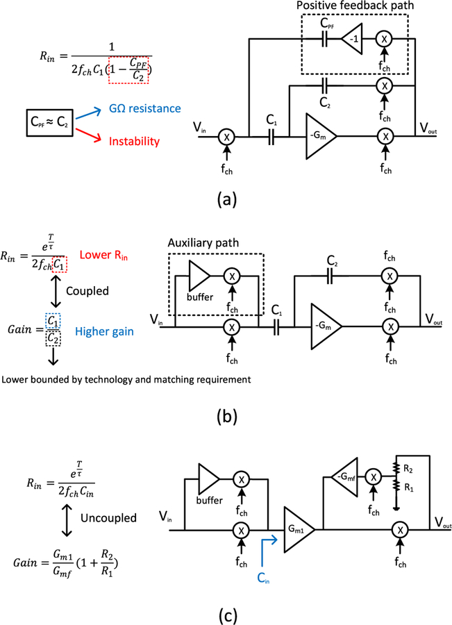
Capacitive feedback amplifiers are commonly used in neural amplifiers because the gain is set accurately by the ratio of capacitors, and the input impedance is high at low frequencies [1–3]. To remove the effect of operational amplifier’s low-frequency noise and DC offset, chopping is used where the low-frequency bio-signals are up-converted to a carrier frequency (fch) away from the DC offset and the flicker noise [4]. The up-converted signal, after bandpass amplification, is down-converted to its original frequency while the DC offset and flicker noise are up-converted away from this signal. However, chopping front-ends suffer from low input impedance at DC due to periodical charging and discharging of the large input capacitors that have values set by the gain considerations. A DC input impedance of larger than 1 GΩ is needed to reduce the input DC current that can damage the tissue [7] or deteriorate the electrodes, especially in longterm implants. Furthermore, given the typically large electrode impedance value (e.g., around 100 MΩ close to DC), a larger input impedance of the neural amplifier is always beneficial to reduce the gain drop due to input voltage division across the impedances which leads to a reduced sensitivity. One way to improve the input impedance of a chopper scheme is by using positive feedback capacitors wired around a traditional capacitive-feedback amplifier [5]. The positive feedback loop can potentially become unstable if GΩ-resistance is desired (Fig. 1a). Past work has shown a self-calibration scheme that acontrols the positive feedback capacitance [6]. An alternative approach is implementing an auxiliary-path pre-charge buffer that reduces the charge supplied by the electrodes to the input capacitors, thus boosting the input impedance [7]. The input DC resistance in these architectures is upper-bounded by the minimum capacitance (C1) which satisfies the gain requirement (Fig. 1b). This work presents a current feedback amplifier architecture which reduces the input capacitance, thereby achieving the highest input impedance reported in the literature for chopper amplifiers (Fig. 1c).
Fig. 1.
Boosting the input impedance of chopping amplifiers: (a) Prior art: positive feedback added to a capacitive feedback chopping amplifier, (b) Prior art: feed-forward axillary path added to the input of a capacitive feedback chopping amplifier, (c) Proposed scheme: feed-forward axillary path added to the input of a current feedback chopping amplifier.
II. System and circuit design
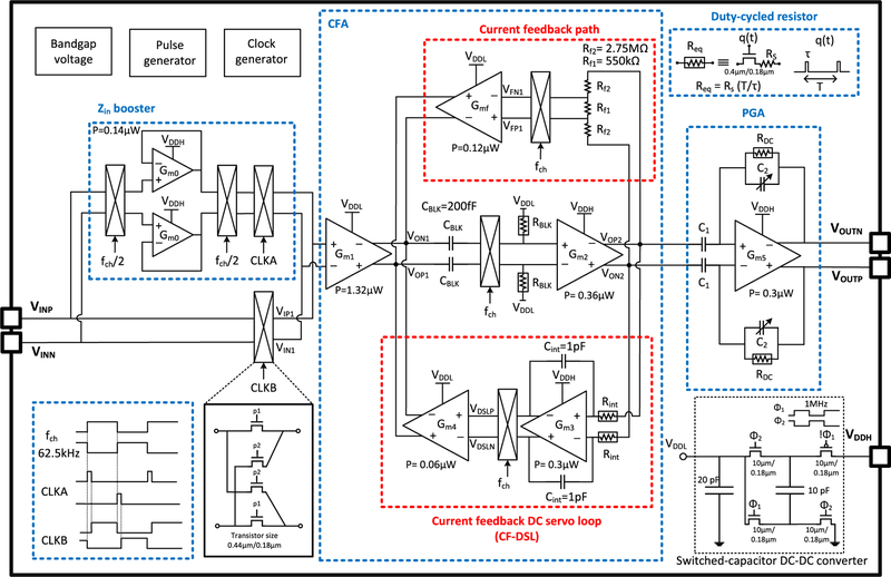
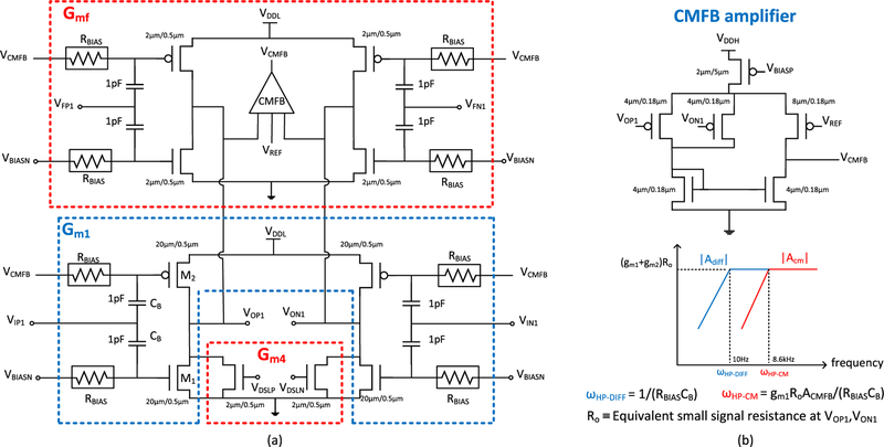
The proposed neural amplifier (Fig. 2) consists of three components, namely, an input impedance (Zin) booster, a current feedback amplifier (CFA), and a programmable gain amplifier (PGA). In the current feedback amplifier, Gm1 and Gm2 form the direct gain path while Rf1 and Rf2 create a resistor divider for the output voltage and the feedback current is generated by Gmf. The gain of this stage is given by (Gm1/Gmf)(1+2Rf2/Rf1), where in this implementation Gm1/Gmf = 10 and Rf2/Rf1 = 5. To ensure a small gain variation in the presence of process mismatches, a common centroid layout is used for trans-conductances Gm1 and Gmf and for resistors Rf2 and Rf1. Inverter-based designs are used to realize Gm1 and Gmf (Fig. 3a). This enables lowering of the supply voltage without sacrificing its bias current. Therefore, noise and power consumption can be lowered simultaneously. Supply voltage VDDL (0.6V) is generated from the main supply voltage VDDH (1.2V) using a 90% efficient on-chip switched-capacitor DC-DC converter.
Fig. 2.
Complete implementation of the chopper stabilized current feedback amplifier
Fig. 3.
Detailed schematic of the front-end trans-conductance amplifier: (a) Gm1 along with the feedback trans-conductance amplifier Gmf and the DC servo loop feedback trans-conductance amplifier Gm4, (b) CMFB amplifier schematic, differential and common-mode transfer functions of Gm1.
The removal of the tail current source in an inverter-based amplifier can drastically reduce the common mode rejection ratio (CMRR), making the differential and commonmode gains equal in all frequencies. However, a commonmode feedback (CMFB) amplifier can mitigate this issue by pushing the common-mode gain high-pass corner ωhP-cm to a higher frequency away from the differential gain high-pass corner ωHP-diff (Fig. 3b). Chopping only upmodulates the differential signal while the common mode signal remains in the baseband. The proposed inverter-based amplifier rejects the common-mode signal for frequencies less than 8.6kHz, while amplifying the upmodulated differential signal at 62.5kHz. The 1–100 GΩ-range resistances (RBLK, RINT, RDC and RBIAS), that are needed for biasing this amplifier, are realized using duty-cycled resistors (DCR) for achieving high linearity and noise performance [7]. Each such DCR consists of a series connection of a polysilicon resistor R, with a value less than 1 MΩ, and an NMOS switch with a gate driven by an independent pulse generator with controllable duty cycle (Fig. 2). Monte Carlo simulations of a DCR formed with a 1 MΩ poly resistor in series with a W/L=400nm/180nm NMOS switch operating at 0.001 duty cycle result in 3σ value of 14 MΩ, which is equivalent to 1.4% variation from the nominal value of 1 GΩ. Duty cycle can vary by 20% due to the global process variations, which is compensated by including tunable capacitor banks in the pulse generators. To remove the DC offset and drift introduced by the electrodes, a current feedback DC servo loop (DSL) is added to the design. The maximum electrode offset that can be tolerated is determined by the ratio of Gm4 / Gm1. In this design, a typical value of 50 mV electrode offset is considered.
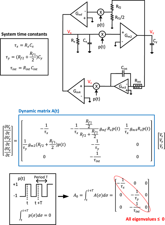
The stability of the proposed amplifier, especially given the two current feedback loops used for setting the gain and removing the input DC offset, must be carefully considered. The conventional techniques for stability analysis of LTI systems (e.g., Nyquist criterion) cannot be used for time-variant periodic systems such as the proposed chopping amplifier. For a time-variant system, a set of state equations (dynamic matrix A(t)) can be derived which describe the system’s behavior in time domain. Starting with the Floquet theorem, it can be shown that the necessary and sufficient condition for stability is that all the eigenvalues of the dynamic matrix have nonpositive real parts [8]. This analysis is performed on the simplified block diagram as shown in Fig. 4. The derived eigenvalues for this system are all non-positive, which ensures the stability of the proposed CFA. An auxiliary path precharge assist [7] is used to facilitate charging and discharging the input capacitance Cin, which is dominated by the Miller capacitance at the input terminal of Gm1. A single-stage transconductance cell is used as a buffer (Gm0) with a duty-cycled current to save power. Required clock signals CLKA and CLKB are generated on-chip using an oscillator and digital delay circuitry consuming 240 nW.
Fig. 4.
Simplified block diagram and stability analysis
The power consumption and footprint of clock generation and the DC-DC converter circuitries, not included in the tabulated results, are well amortized across multiple amplifiers of a multi-channel neural implant. A programmable gain amplifier (PGA), following the chopper front-end, amplifies the signal up to 20 dB. Capacitor C1 has a fixed value of 1 pF and capacitor bank C2can be programmed to provide 2 – 20 dB of variable gain.
III. Measurement results
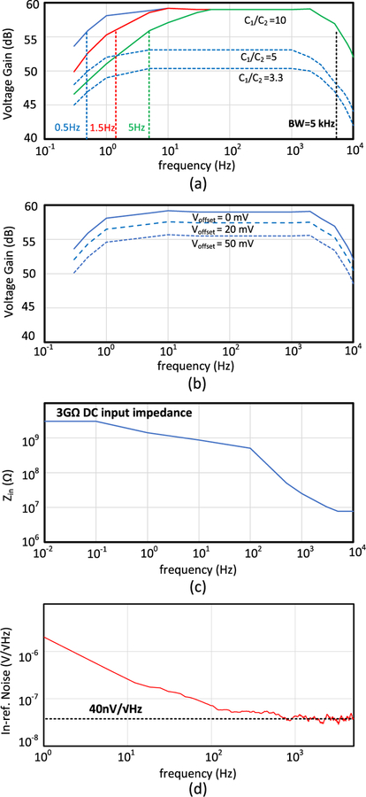
The chopper CFA amplifier was fabricated in a 0.18μ m CMOS technology (Fig. 5). The DC-DC converter achieves 90% efficiency. The entire amplifier consumes 2.6 μW from a 1.2 V supply. Fig. 6 shows measured voltage gain, input impedance, and input-referred noise versus frequency. The transfer functions for different gain and high-pass corner settings as well as for different input offset voltages are shown. The chopped offset voltage appears at the amplifier input as a large signal, which compresses the apparent small signal gain of the amplifier due to the 3rd-order nonlinearities. One downside of the proposed scheme is that, the open-loop nature of Gm1 limits the overall linearity; consequently, compared with capacitive-feedback amplifiers, the total harmonic distortion (THD) of this scheme is worse. The pulse width for RINT is changed from 0.7–7 ns to adjust the high-pass corners. The input impedance reaches a maximum of 3 GΩ below 0.1 Hz. To measure the input impedance, a pair of off-chip 100 MΩ resistances are placed in series with the differential inputs and a pair of high-impedance voltage buffers with >1 TΩ input resistance are used to tap-off the voltage at the amplifier input. The measured buffered voltage reflects the voltage divider between the amplifier input impedance and the off-chip 100 MΩ series resistances. Table I summarizes the performance of this neural amplifier front-end in comparison with the current state-of-the-art reported designs. The combination of voltage gain, noise, input impedance, area and power consumption are the best for this design, confirming the usefulness of the proposed scheme.
Fig. 5.
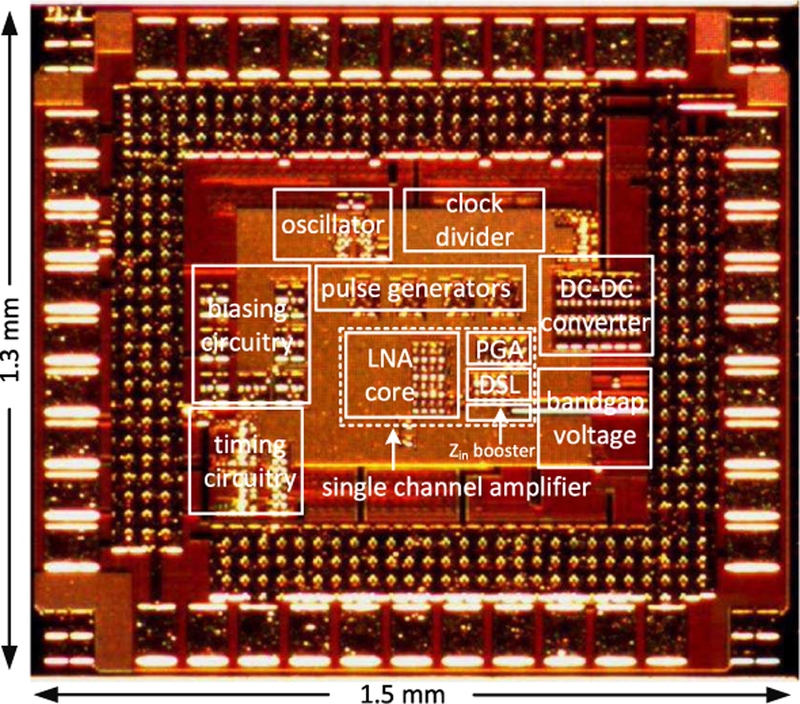
Die micrograph
Fig. 6.
Measured transfer functions: (a) voltage gain with different settings, (b) voltage gain variation as a function of the input offset voltage, (c) input impedance, (d) input referred noise.
TABLE I.
Performance summary and comparison with state-of-the-art bio-potential amplifiers
| This work | [1] JSSC ‘18 | [2] JSSC ‘18 | [4] JSSC ‘15 | [5] ISSCC ‘16 | [6] CICC ‘17 | [7] JSSC ‘17 | ||
|---|---|---|---|---|---|---|---|---|
| Application/Signals | AP, LFP | AP, LFP | AP, LFP | LFP | EEG, LFP | ECG | AP, LFP | |
| Technology | 180 nm | 180 nm | 180 nm | 65 nm | 180 nm | 180 nm | 40 nm | |
| Supply (V) | 0.6, 1.2 | 1.0 | 0.5, 1.0 | 0.5 | 0.2, 0.8 | 0.8 | 1.2 | |
| Channels | 1 | 1 | 128 | 64 | 1 | 1 | 8 | |
| Input Referred Noise (μVrms) Power/Ch (μW) |
AP: 3.2 LFP: 2.0 |
5.5 (250 Hz −10 kHz) |
3.32 (0.5 Hz −12.7 kHz) |
1.3 (1 Hz −500 Hz) |
0.94 (0.5 Hz – 670 Hz) |
8.26 (1 Hz – 400 Hz) |
AP: 5.3 LFP: 1.8 |
|
| 2.6(a) | 0.25 | 1.22(c) | 2.3 | 0.79 | 0.255 | 2.8 | ||
| NEF |
AP: 3.2 LFP: 9.9 |
1.07 | 3.02 | 4.76 | 2.1 | 7.01 | AP: 4.4 LFP: 7.4 |
|
| 3dB-Bandwidth | 0.5 Hz - 5 kHz | 4 Hz-10 kHz | 0.4 Hz-10.9 kHz | 1 Hz - 500 Hz | DC - 670 Hz | 400 Hz | 0.1 Hz - 5 kHz | |
| Gain (dB) | 41–59 | 25.6 | 37.5–52.9 | N/A | 50.8–57.8 | 34 | 25.7 | |
| CMRR (dB) THD (%) Area/Ch (mm2) |
70 | 84 | >60 | 88 | 85 | 66 | 77 | |
|
1.7(b) (1.0 mVpp,in 1kHz) |
N/A | 0.02(d) (3 mVpp,in 1 kHz) |
0.4 (1 mVpp, in40Hz) | 0.3(b) (1.5 mVpp,in 100Hz) |
N/A | 0.3 (80 mVpp,in 1 kHz) |
||
| 0.08(a) | 0.29 | 0.05 | 0.025 | 1.0 | 0.581 | 0.069 | ||
| Zin | DC | 3.0 GΩ | ∞ | ∞ | 28 MΩ | 116 MΩ(e) | 200 GΩ | 1.6 GΩ |
| 100 Hz | 500 MΩ | 200 MΩ | 80 MΩ | N/A | N/A | 10 GΩ | 800 MΩ | |
| Electrode Offset Removal | Current feedback DSL | AC coupled | AC coupled | DAC feedback DSL | No | DSL | RC integrator DSL | |
Action Potential (AF): ZUU Hz - quoted bandwidth, Local Field Potential (LFP): l Hz - 200 Hz.
excludes clock and DC-DC converter circuitries
maximum gain setting,
LNA and PGA blocks are considered only
LNA stage only
estimated.
IV. Conclusion
A compact high-input-impedance, chopper-stabilized, current-feedback neural amplifier with adjustable gain and high-pass corner has been demonstrated in a 180nm CMOS process. The proposed architecture achieves the highest input impedance reported by the literature for a bio-signal chopper amplifier, while maintaining a competitive noise and power performance.
Acknowledgment
The authors appreciate the technical discussions and support of research collaborators Prof. Ellis Meng, Prof. Dong Song, Prof. James Weiland, and their research group members.
This work was partially supported by the NSF under award number 1343193 and the NIH under project number 5U01NS099703–03.
References
- [1].Shen L, Lu N and Sun N, “A 1-V 0.25- μ W inverter stacking amplifier with 1.07 noise efficiency factor,” IEEE J. Solid-Sate Circuits, vol. 53, no. 3, pp. 896–905, Mar. 2018. [Google Scholar]
- [2].Park SY, Cho J, Na K and Yoon E, “Modular 128-channel Δ-ΔΣ analog front-end architecture using spectrum equalization scheme for 1024-channel 3-D neural recording microsystems,” IEEE J. Solid-Sate Circuits, vol. 53, no. 2, pp. 501–514, Feb. 2018. [Google Scholar]
- [3].Lopez CM, Mitra S, Putzeys J, Raducanu B, Ballini M, Andrei A, Severi S, Welkenhuysen M, Van Hoof C, Musa S and Yazicioglu RF, “A 966-electrode neural probe with 384 configurable channels in 0.13μm SOI CMOS,” IEEE ISSCC, 2016. [DOI] [PubMed]
- [4].Muller R, Le HP, Li W, Ledochowitsch P, Gambini S, Bjorninen T, Koralek A, Carmena JM, Maharbiz MM, Alon E and Rabaey JM, “A minimally invasive 64-channel wireless μECoG implant,” IEEE J. Solid-Sate Circuits, vol. 50, no. 1, pp. 344–359, Jan. 2015. [Google Scholar]
- [5].Yaul F and Chandrakasan A, “A Sub-μ W 36nV/√Hz Chopper Amplifier for Sensors Using a Noise-Efficient Inverter-Based 0.2V-Supply Input Stage,” IEEE ISSCC, 2016.
- [6].Lee J, Kim H and Cho S, “A 255nW ultra-high Input impedance analog frontend for non-contact ECG monitoring,” IEEE CICC, 2017.
- [7].Chandrakumar H and Markovic D, “An 80-mVpp linear-input range, 1.6- GΩ input impedance, low-power chopper amplifier for closed-loop neural recording that is tolerant to 650-mVpp common-mode interference,” IEEE J. Solid-Sate Circuits, vol. 52, no. 11, pp. 28112828, Nov. 2017. [Google Scholar]
- [8].Chen G, “Stability of nonlinear systems,” in Wiley Encyclopedia of Electrical and Electronics Engineering, Webster JG, Ed. New York: Wiley, pp. 627–642, 2000. [Google Scholar]


