Abstract
CMOS microelectrode arrays (MEAs) can record electrophysiological activities of a large number of neurons in parallel but only extracellularly with low signal-to-noise ratio. Patch clamp electrodes can perform intracellular recording with high signal-to-noise ratio but only from a few neurons in parallel. Recently we have developed and reported a neuroelectronic interface that combines the parallelism of the CMOS MEA and the intracellular sensitivity of the patch clamp. Here, we report the design and characterization of the CMOS integrated circuit (IC), a critical component of the neuroelectronic interface. Fabricated in 0.18-μm technology, the IC features an array of 4,096 platinum black (PtB) nanoelectrodes spaced at a 20 μm pitch on its surface and contains 4,096 active pixel circuits. Each active pixel circuit, consisting of a new switched-capacitor current injector—-capable of injecting from ±15 pA to ±0.7 μA with a 5 pA resolution—-and an operational amplifier, is highly configurable. When configured into current-clamp mode, the pixel intracellularly records membrane potentials including subthreshold activities with ∼23 μVrms input referred noise while injecting a current for simultaneous stimulation. When configured into voltage-clamp mode, the pixel becomes a switched-capacitor transimpedance amplifier with ∼1 pArms input referred noise, and intracellularly records ion channel currents while applying a voltage for simultaneous stimulation. Such voltage/current-clamp intracellular recording/stimulation is a feat only previously possible with the patch clamp method. At the same time, as an array, the IC overcomes the lack of parallelism of the patch clamp method, measuring thousands of mammalian neurons in parallel, with full-frame intracellular recording/stimulation at 9.4 kHz.
Keywords: current clamp, extracellular recording, integrated circuits, intracellular recording, microelectrode array, nano-bio interface, nanoelectrode array, neurobiology, neurons, switched capacitor, voltage clamp
I. Introduction
CMOS microelectrode arrays (MEAs) have served as an important tool in neurobiology with their ability to record membrane potentials from a large number of neurons, with the state of the art featuring as many as 10,000’s recording channels [1]–[14]. But this neuronal recording by the CMOS MEA is an extracellular technique. The voltage it records outside the neuron is a highly attenuated and filtered version of the actual membrane potential inside the neuron: e.g., action potentials (APs) with intracellular amplitudes of ∼100 mV are attenuated to below ∼100 μV at the extracellular electrode and their intracellular duration of ∼ 10 ms is reduced to as short as 100 μs at the extracellular electrode [12]. Given such a large attenuation through the extracellular neuron-microelectrode interface, the CMOS MEA cannot record small but critical synaptic events, such as post synaptic potentials (PSPs), whose intracellular amplitudes are less than ∼5 mV. Another related drawback of the CMOS MEA is the inability for concurrent stimulation and recording of a neuron through the same electrode, as an extracellular stimulation signal needed is over 103× larger than the extracellularly recorded signal [15].
In contrast, the patch clamp technique, the gold standard of high-fidelity electrophysiological recording, directly accesses the intracellular solution of a neuron with no attenuation by mechanically puncturing its membrane followed by a tight sealing [16]. The resulting intracellular recording has a far higher sensitivity than the CMOS MEA and can routinely measure synaptic activities. This intracellular recording can be also simultaneously performed with stimulation in the form of current clamp (membrane potential recording with current injected) or voltage clamp (membrane current recording with voltage applied). The current and voltage clamp modes are used for a variety of electrophysiological interrogation of neurons. For example, the current clamp recording of PSPs can find synapses and the voltage clamp, which was used for the first measurement of currents of single ion-channel molecules [17], can characterize the effect of drugs on ion channels. This highly sensitive patch clamp electrode, however, cannot be scaled into a dense array like the CMOS MEA, and only ∼10 parallel patch neuron recordings have been possible so far [18].
Recently nano and micro electrodes of three dimensional structure were studied for the possibility of intracellular access [19]–[30]. Some of them are also scalable, defined by top-down fabrication, and so have been hoped for combining the intracellular sensitivity of the patch clamp and the parallelism of the CMOS MEA. But only a few of them [22], [23], [26], [27] could couple intracellularly with mammalian neurons and even then, only on a single or few neuron basis, and without the current/voltage-clamp configurations, thus lacking the capability for simultaneous recording and stimulation through the same electrode.
We have very recently developed a scalable, 64 × 64 = 4,096 platinum black (PtB) nanoelectrode array on a CMOS integrated circuit (IC), which bridges the previous gap between the intracellular sensitivity of the patch clamp and the parallelism of the CMOS MEA and performs massively parallel intracellular recording from thousands of connected mammalian neurons [31]. The CMOS IC realizes current/voltage-clamp electronics for each of the 4,096 sites, or pixels. At an individual pixel, both the surface PtB nanoelectrode interfacing with a neuron and the underlying CMOS voltage/current clamp electronics operating the PtB nanoelectrode are critical for the stable intracellular recording/stimulation of the neuron. At the same time, its arrayed operation gives rise to the parallelism.
In [31], we reported network-wide intracellular recording with this chip and its application in synaptic connectivity mapping and high-throughput drug screening. The present paper complements [31], reporting the design of the CMOS IC, describing in detail how it enables the intracellular neuronal recording with simultaneous stimulation using current/voltage clamp, a feat only previously possible with the patch clamp technique, and how it parallelizes such high-fidelity recording across the array, overcoming the limitation of the patch clamp.
Section II overviews the CMOS IC. Section III presents the pixel circuit and its current- and voltage-clamp configurations. Section IV presents the new, switched-capacitor based current injector, a crucial pixel circuit component. Sections V and VI present electrical and electrophysiological characterizations.
II. Overview of the CMOS IC
Since we seek to intracellularly record and stimulate a large number of neurons, we build a dense array of electrodes capable of intracellular access with the electrode pitch comparable to mammalian neuron dimensions (20–40 μm diameter somas) on top of a CMOS IC that integrates electronics for current- and voltage-clamp measurements at each pixel electrode. Specifically, the IC, fabricated in a dedicated 0.18-μm, 1-poly, and 6-metal wafer run, contains an array of 4,096 surface Al pads at the chip center (pad-to-pad pitch: 20 μm), connected to 4,096 active pixel circuits distributed in the 4 peripheral quadrants (1,024 circuits per quadrant) (Fig. 1a). PtB electrodes are post-fabricated on each Al pad for intracellular access [31]. The spaces between the quadrants are used for the wiring from electrodes to pixel circuits. Each pixel circuit contains a switched capacitor based current injector and an op-amp (Fig. 1b) to create a current or voltage clamp configuration (Sec. III). The IC area is 10 × 20 mm2. We place only one IC in each reticle occupying 20 × 20 mm2 to allow a 5 mm handling area on each side of the IC for the post fabrication of PtB electrodes. These handling areas are diced away before wire bonding and packaging [25], [31].
Fig. 1.
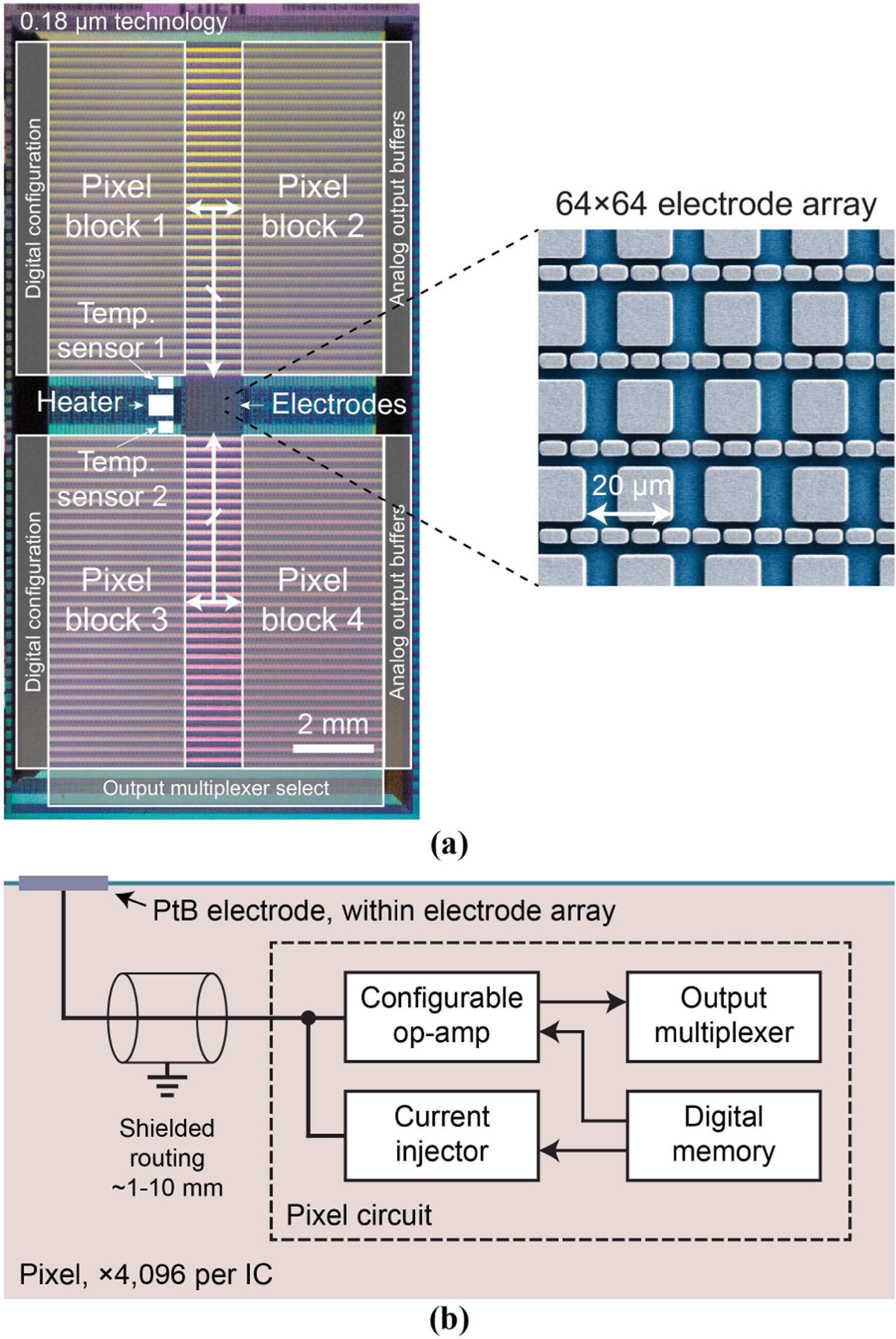
(a) Chip micrograph (10 × 20 mm2) along with a false colored scanning electron microscope (SEM) image of the 4,096 Al pads before post fabrication of PtB electrodes. (b) Block diagram of an active pixel circuit.
By separating the electrode array region in the center from the active pixel circuit region in the 4 peripheral quadrants, we achieve both the dense 20 μm pitch for the electrode array for high spatial resolution and the large 100 × 250 μm2 area for each active pixel circuit for high configurability and low noise. This layout strategy combines the concepts of high-fidelity peripheral electronics from the switched matrix CMOS MEAs [3], [8], [11], [13] and the full-frame readout of the active-pixel sensor (APS) CMOS MEAs [1], [2], [7], [14].
The metallic routing from a pixel circuit to its electrode has a length of 1 ∼ 10 mm, depending on the location of the pixel circuit and its electrode. To mitigate the capacitive coupling between adjacent routings, we surround each routing with ground shields (Fig. 2, left). This reduces the cross-coupling capacitance to < 1 fF per routing, virtually ensuring no cross-contamination between different electrode signals (Section V.D). We minimize the parasitic capacitance Cp,r between an individual routing and its shield by gradually increasing the spacing between them, as the density of the routings decreases further away from the electrode array. Cp,r is ∼1–2 pF in electric field simulations (Fig. 2, right for the densest routings). The routings and shields use 4 of the available 6 metal layers and occupy ∼1.5 × 20 mm2 in total.
Fig. 2.
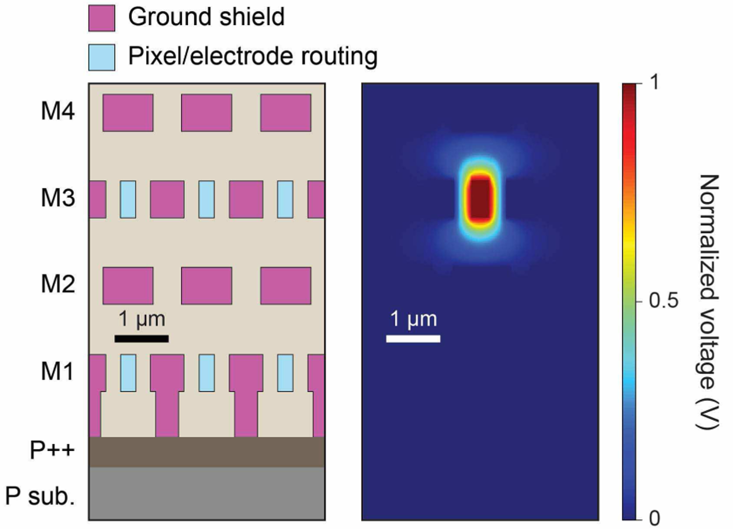
(left) Cross section of the densest pixel circuit to electrode routings using the bottom four metal layers; M5-M6 are used for other routings. (right) Electric field simulation to calculate the routing parasitic capacitance.
To enable accurate temperature regulation, the IC contains two temperature sensors (based on the voltage differential between two diode branches of different sizes, 1:146 ratio, biased at the same current) and a heater (a 10-Ω poly silicon resistor capable of dissipating 1.3 W) adjacent to the electrode array (Fig. 1a). They regulate the temperature of the IC to 34–37°C for cell health (Section V.A).
The design of this IC with the particular choice of the architecture, building blocks, and target performance is guided by our goal to demonstrate the unprecedented massive parallelism in intracellular recording of neurons. For example, we focus our design efforts significantly on realizing the front-end current/voltage clamp capability in each active pixel circuit, as it is essential for robust intracellular access into neurons; on the other hand, for the back-end digitization that is not fundamental to the key demonstration goal, we choose to use commercially-available high-precision analog-to-digital converters (ADCs) in order to accelerate the chip development. To drive such off-chip electronics, we implement high-speed analog multiplexers on chip. They require large bias currents to operate at frequencies in excess of 1 MHz, but in our in vitro setting the associated heat readily sinks through the open well of solution on the chip. In fact, we actually need an explicit heating of the solution to keep the cells at the temperature around 35 °C. This is in contrast to implantable applications [32], where an IC insulated by biological tissue should maintain low power density to prevent tissue damage.
III. The Active Pixel Circuit
Figure 3a shows the schematic of the active pixel circuit. Its main components are a switched capacitor current injector (Sec. IV) and an op-amp with configurable negative feedback networks, both of which are connected to the same PtB electrode of the pixel. It also contains a transparent latch digital memory and an output multiplexer (shared by 128 pixels per multiplexed analog output). The pixel circuit contains many transmission gate switches, controlled by the digital memory programmable in real time at up to ∼10 MHz. Many of these switches are in the op-amp negative feedback networks, making the closed-loop amplifier highly configurable. Four voltage nodes, Vs,1 through Vs,4, can be connected to various voltage signals or bias references from off-chip electronics, supporting the high configurability as well as various tests. Of the pixel circuit area of 0.025 mm2 (Fig. 3b), the op-amp takes the largest part due to large transistors (Fig. 3c, left) for minimizing noise [33]. A dedicated bias network is included for each pixel, as opposed to a global bias, to help isolate the 4,096 op-amps. The current injector occupies only ∼0.003 mm2, almost an order of magnitude smaller than standard current injectors used in MEAs [6], [9], [11], [13], attesting to the advance of our novel design (Sec. IV).
Fig. 3.
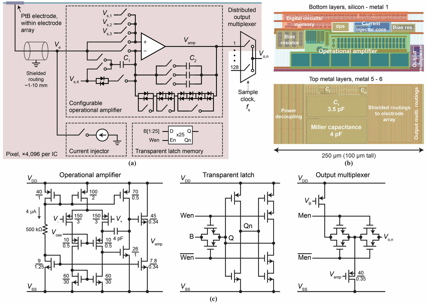
(a) Active pixel circuit schematic. The switches (transmission gates) are controlled by the transparent latch memory to configure the pixel for experiments. C1 = 3.5 pF; C2 has the options of adding any of ∼5 fF, ∼20 fF, and ∼100 fF. (b) Active pixel circuit layout. Metal-insulator-metal capacitors are identified on the topmost metal layers. (c) Transistor-level schematics of various pixel components, in particular, op-amp (left), transparent latch (middle), and output multiplexer (right); the schematic of the current injector is shown in detail in Fig. 7.
For intracellular recording/stimulation, we operate the pixel circuit of Fig. 3a in pseudo current or voltage clamp mode (Fig. 4), named after the similar configurations of the patch clamp. ‘Pseudo’ emphasizes that our intracellular interface has a finite attenuation, unlike the patch clamp, as seen below.
Fig. 4.
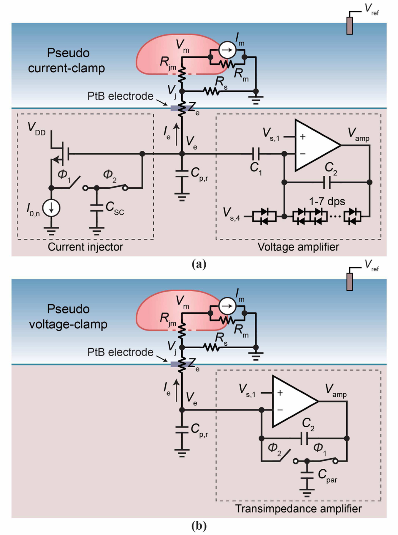
(a) The pCC pixel configuration. (b) The pVC pixel configuration.
A. Pseudo Current-Clamp (pCC) Configuration
The pseudo current-clamp (pCC) mode (Fig. 4a) is obtained from Fig. 3a by operating the high output impedance current injector in parallel with the op-amp with the negative feedback configured as a high input impedance voltage amplifier. The current injector runs a current Ie through the electrode. This continuously injected Ie (typically on the order of −1 nA) causes and sustains the membrane permeabilization in a neuron to initiate and maintain intracellular coupling [31]. Another crucial role of this current injection is to compensate the leakage current from within the neuron that inevitably arises due to the membrane permeabilization. At the same time, the voltage amplifier concurrently measures the electrode voltage, Ve, which is an attenuated version of the membrane potential, Vm. In this way we intracellularly record membrane potentials (APs and PSPs) of the neuron. This operation is akin to the patch clamp’s current clamp recording.
The voltage amplifier is a bandpass configuration, traditionally used for low-noise neural recordings [33] (Fig. 4a). Its passband gain from Ve to the amplifier output Vamp is the ratio of the feedback capacitors −C1/C2. This is tunable: C1 is 3.5 pF but C2 can be any addition of ∼5, ∼20, and ∼100 fF (Fig. 3a). The amplifier bandwidth covers the electrophysiological spectral range: ∼1 Hz to 5 kHz [34]. The low frequency pole, f1 ∼ 1 Hz, is set by C2 in parallel with the large resistance of feedback antiparallel diode pairs (dps) (options for 1–7 dps; Fig. 3a) biased near zero current. The more the dps, the less the voltage drop on each dp, reducing the nonlinearity and increasing the resistance. These dps are realized using p-contacts within an n-well and contain parasitic reversed biased pn diodes to the substrate and corresponding leakage currents. An additional dp tapped to Vs,4 sets a small current to tune the DC level of Vamp to overcome these leakage currents and to fine tune the feedback resistance, which we discuss experimentally in Sec. V.C. The high frequency pole, f2, is set by the gain bandwidth product of the amplifier.
In the pCC recording, a change of the membrane potential, Vm, modulates the electrode voltage, Ve, according to:
| (1) |
Rs is the seal resistance, Rjm is the junctional membrane resistance, and Z1, Zp,r and Ze are the impedances of C1, Cp,r, and the PtB electrode. The approximation in the last step of Eq. (1) is due to , which holds as the surface roughness thus large surface area of the PtB electrode greatly reduces Ze [Sec. V-D]. The front-end attenuation of Eq. (1) precedes the amplifier gain, contrasting the patch clamp’s current clamp that has no such front-end attenuation (hence the prefix, ‘pseudo’ in our current clamp). But as seen shortly, this attenuation is far less than that of the extracellular recording.
For stimulation, we change Ie to modulate Vm according to:
| (2) |
where Rm is the membrane resistance. Here we have assumed , which holds for most nanoelectrodes (typical values: Rs < 100 MΩ, , Rm ∼ 100 MΩ).
Equations (1) and (2) show that a reduction of Rjm or an increase in Rs improves the recording amplitude and the ability to manipulate Vm for stimulation. Case in point, the membrane permeabilization (intracellular access) induced by the aforementioned injection of Ie reduces Rjm to decrease the attenuation of Eq. (1) by 1∼2 orders: APs are measured from rat neurons with ∆Ve of 1 ∼ 30 mV [31], contrasting MEA extracellular recording of APs in the range of 10 ∼ 100 μV. Overall, the pCC allows intracellular recording of membrane potentials of a neuron with a current injection, where the current injection can be also used for concurrent stimulation. Finally, note only a small fraction (∼1–10%) of Ie ∼ −1 nA enters the permeabilized neuron, as .
Recently a CMOS MEA [6] as well as our previous version of the CMOS nanoelectrode array [25] intracellularly recorded the membrane potential of cardiomyocytes without using the pCC but by applying a voltage to an electrode followed by a voltage recording. This voltage application also produces an electrode current to permeabilize the cell membrane for intracellular access. But since the voltage application and voltage recording cannot be simultaneous, the electrode current is absent during the recording, and hence, the permeabilization-induced leakage from the cell cannot be compensated during the recording. This still did not prevent the intracellular recording of the membrane potentials of cardiomyocytes, as the tissue of the cardiac cells is electrically more robust due to their gap junction connections. But this voltage-application voltage-recording approach deficient in leakage compensation cannot achieve stable intracellular recording of neuronal membrane potentials, as neurons are electrically isolated via chemical synapses and are therefore far more adversely affected by the leakage and the resulting depolarization.
B. Pseudo Voltage-Clamp Configuration
The pseudo voltage-clamp (pVC) mode (Fig. 4b) is obtained by disconnecting the current injector and configuring the feedback loop of the op-amp to form a transimpedance amplifier. The feedback resistance of the transimpedance amplifier is a switched capacitor, which utilizes the switches in parallel to the feedback dps and the parasitic capacitance Cpar ∼35 fF of the intermediate node between the sets of 2 dps and 4 dps (Fig. 3a). These switches are controlled in real time using the memory with non-overlapping clock phases Φ1 and Φ2. We set the effective resistance RTIA = 1/ fTIACpar of the switched capacitor typically around ∼700 MΩ using a switching frequency fTIA of ∼ 40 kHz. The high-frequency pole of the transimpedance amplifier is set by the feedback capacitance C2 in parallel with RTIA.
In contrast to the commonly used integrate and reset scheme, which offers the lowest noise option for current measurement [35], the feedback switched capacitor allows for sampling of all pixels via the multiplexer regardless of their sampling position as the output voltage is never completely reset. Rather, a packet of feedback charge, ∆Qfb = VampCpar, is switched from the output to the negative terminal of the amplifier to ‘soft-reset’ the voltage across C2, which reaches a steady state across a switching period, 1/ fTIA, when it is equal to the transimpedance amplifier input current, Iin = ∆Qfb/ fTIA. The noise of this configuration is comparable to the integrate and reset scheme, as the input current is integrated across C2 [35], except we observe significantly more noise from pixels sampled during Φ1 due to additional leakage current from the 3 dps in parallel to the used switch (Fig. 3a) (Section V.C).
The pVC mode utilizes the transimpedance amplifier in applying a voltage Vs,1 = Ve to the electrode and simultaneously measuring the electrode current Ie. The bias point of Ve is adjusted to set the bias value of Ie at −1 nA, which induces membrane permeabilization for intracellular access. Then the modulation of Ve is used as a voltage stimulation to induce a change of the membrane potential Vm:
| (3) |
where we have used , and Rm, and . The resulting membrane current (ion channel current such as Na+ spikes) ∆Im modulates the electrode current in the range of ∼100 pA to 1 nA [31] according to
| (4) |
This ∆Ie is measured by the transimpedance amplifier. ∆Ie is an attenuated version of ∆Im and contrasts the patch clamp’s voltage clamp that has no such front-end attenuation (and hence the prefix, ‘pseudo’ for our voltage clamp). But the attenuation factor is greatly reduced due to the reduction of Rjm with the intracellular access (membrane permeabilization with the injection of the bias value of Ie), just like in the pCC case. On the other hand, unlike the pCC, increasing Rs does not improve either the ability to record or stimulate to the first order: as , and Rm, Vj is effectively connected to the pseudo-ground of the amplifier’s negative terminal which eliminates shunted membrane current through Rs. Nonetheless, a small Rs will increase the bias value of Ie for a given Ve and also decrease recording/stimulation signal transfer if Rs ∼ Ze.
IV. A Switched-Capacitor Based Current Injector
A key building block in the pixel circuit that enables the pCC intracellular recording is the current injector. Our novel design meets the demands of pA-range current precision needed for the membrane permeabilization, high output impedance to hold an injected current at a nearly constant and not to interfere with voltage signal amplification, and a small area such that it can be integrated in each of the 4,096 pixels.
A. Basic Topology and Operating Principle
In Fig. 5a, a capacitor CSCswitched between voltages V1 and VOUT (V1 > VOUT) with non-overlapping clock phases and of frequency fSC acts as a resistor Reff = 1/ fSCCSC. The output current into VOUT, averaged over a clock period, is given by . As fSC can be varied over many orders of magnitude, can assume a wide range of values, with its minimum value comfortably falling into the pA region. For example, with CSC = 30 fF, V1 − VOUT = 0.6 V, and fSC increasing from 1 kHz over many orders of magnitude, can be tuned up from 18 pA over the same orders of magnitude. If this switched capacitor drives an electrode immersed in an electrolyte modeled as a Faradaic resistor RL in shunt with a double layer capacitor CL (Fig. 5a), the injected cannot be fixed at a constant as VOUT varies with time. The corresponding small-signal output impedance, , is Reff = 1/ fSCCSC.
Fig. 5.
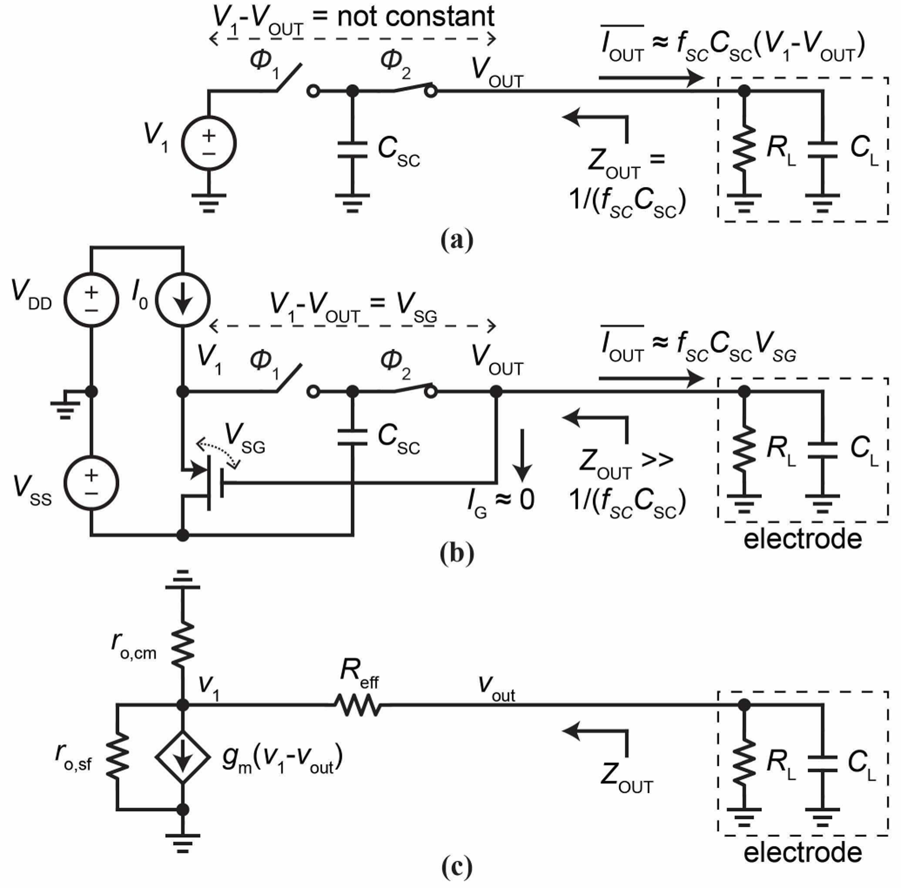
(a) Switched capacitor driving an electrode. (b, c) Switched capacitor with active circuit to increase output impedance and its small-signal model.
To increase ZOUT substantially, we can build a source follower circuit around the switched capacitor like in Fig. 5b to set V1 - VOUT at a fixed value: the V1 and VOUT nodes of the switched capacitor are connected to the source and gate of the PMOS transistor. V1 then follows VOUT to maintain V1 - VOUT at VSG, the source-gate voltage of the transistor. In the absence of channel length modulation, VSG is fixed at a constant value by the bias current I0 and independent of VOUT. In this ideal case, is perfectly independent of VOUT and can be set by fSC and CSC to a constant value. Correspondingly, ZOUT = ∞. In the realistic case with the transistor channel length modulation, VSG does vary with VOUT but only weakly, so exhibits only a small dependence on VOUT. The corresponding ZOUT calculated with the small-signal model of Fig. 5c is:
| (5) |
where ro,sf and ro,cm are the output resistances of the PMOS transistor and the current (I0) bias circuit, respectively, and gm is the transconductance of the PMOS transistor. The second line is approximated by setting without losing essence and by using . As seen, ZOUT is greatly boosted from by a factor of gmro/2.
B. Transient Dynamics
We now discuss the transient behaviour of the switched capacitor current injector of Fig. 5b. During a clock phase Φ1, CSC is disconnected from VOUT and connected to V1 via the switch on-resistance . Throughout this Φ1 phase, VOUT decays with a slow time constant of the load, τL = RLCL, and V1 follows this decay to maintain V1 = VOUT + VSG (Fig. 6a). In contrast, at the onset of the phase Φ1, the switched capacitor voltage, VSC, makes a rapid upward transition from VOUT to V1 = VOUT+ VSG (Fig. 6a), rapidly charging CSC (time constant: ) with ∆QSC = CSC∆VSC = CSCVSG.
Fig. 6.
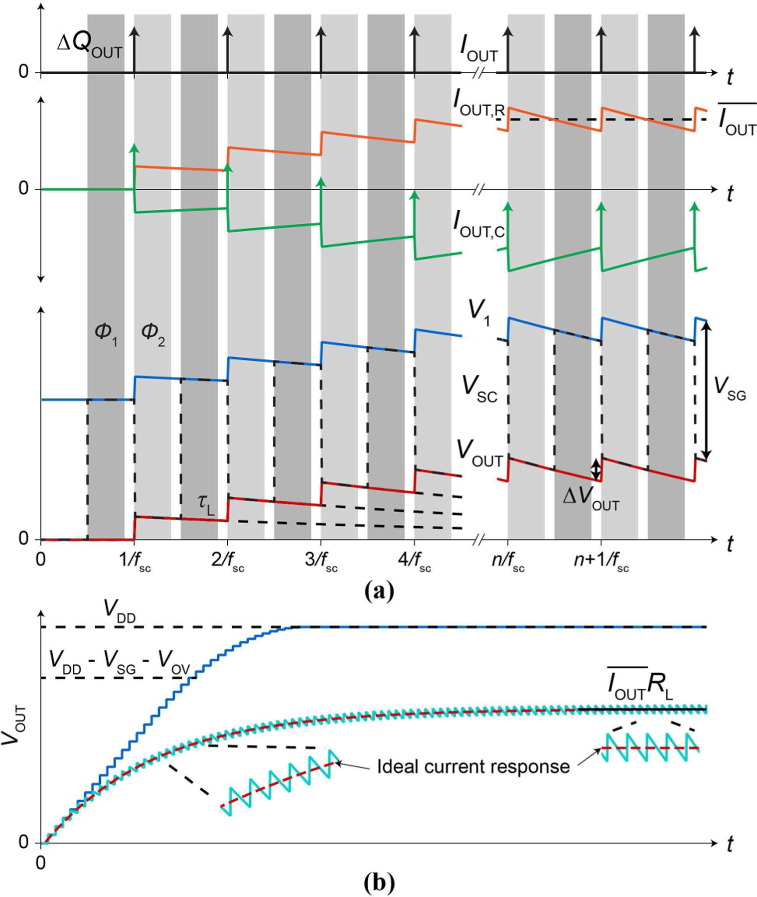
(a) Timing diagram for IOUT, IOUT,R IOUT,C, and V1, VSC, VOUT. (b) VOUT(t) for the RLCL load (cyan, solid) in juxtaposition with VOUT(t) for a CL-only load (blue, solid). The response of the RLCL load to an ideal step current is overlaid (red, dashed) for comparison.
During the subsequent clock phase Φ2, CSC is disconnected from V1 and connected to VOUT via RSW. This re-configuration rapidly redistributes the charge ∆QSC = CSCVSG between CSC and CL with a fast time constant , discharging CSC (lowering VSC) and charging CL (raising VOUT) until VSC = VOUT (Fig. 6a). The resulting change of the output voltage, ∆VOUT, is
| (6) |
These changes of VSC and VOUT (V1 follows VOUT to maintain the difference VSG) occur rapidly during the very early part of the phase Φ2 due to the short time constant τ2 (Fig. 6a). The charge packet injected to CL during the charge redistribution in the early part of Φ2 is ∆QOUT = CL∆VOUT. The output current IOUT is due to this charge packet injection, and its average over a clock period is given by
| (7) |
which is consistent with the calculation of Sec. IV-A.
With repeated clock cycles VOUT is then a sequence of a rapid ∆VOUT up-step (time constant τ2) followed by a slow decay (time constant τL) (Fig. 6a). If we break down IOUT into current IOUT,R through RL and current IOUT,C through CL (IOUT = IOUT,R + IOUT,C ) in phase Φ2, the rapid charging of CL in the beginning of Φ2 is described by IOUT ≈ IOUT,C > 0, while the background slow discharging of CL through RL is described by -IOUT,C ≈ IOUT,R (IOUT,C < 0) with IOUT ≈ 0 (Fig. 6a). In the initial clock cycles, the charging of CL by the charge packet injection ∆QOUT = CL∆VOUT per clock cycle exceeds its discharging through RL per clock cycle thus VOUT overall rises, but once CL is sufficiently charged at later clock cycles, its charging and discharging balance each other, and VOUT reaches a plateau (except voltage ripples) (Fig. 6a, bottom; Fig. 6b). This evolution of VOUT into the steady state, ignoring the ripples, can be quantified by evaluating VOUT at t = n/ fSC or at the end of n-th clock phase Φ2 as follows,
| (8) |
where we have used and Eqs. (6) and (7). This converges to in steady state (Fig. 6b), i.e., in the steady state, flows into the electrode to charge CL and then exactly the same amount of charge leaks out through RL as expected. This is equivalent to flowing through RL. In fact, the overall voltage response of the RLCL load to the switched-capacitor current injector captured by Eq. (8), ignoring the ripples (∆VOUT of Eq. (6)), is identical to the voltage response of the RLCL load to an ideal step current with a magnitude (Fig. 6b). This justifies our current injector as a constant current injector. The foregoing discussion has assumed (VOV: overdrive voltage of the current mirror transistor); if will start to roll off and be clipped at VDD (Fig. 6b).
In the pCC mode, the current injector is connected to the electrode (so Ve = VOUT and Ie = IOUT) and runs in parallel with the voltage amplifier (Fig. 4a) where ∆VOUT = 0.1 ∼ 50 mV for CL = 1 ∼ 100 pF. This ripple voltage could interfere with the recording of ∆Ve = 1 ∼ 30 mV. We minimize this interference using clock synchronization [Section IV-D].
C. Implementation
The actual switched-capacitor based current injector we implement is shown in in Fig. 7a. It can inject both positive and negative currents. The polarity is controlled by turning on either current source I0,p or I0,n, to reduce the circuit to either Fig. 7b for positive injection, , or Fig. 7c for negative injection, . For pCC recording, we use the NMOS configuration of Fig. 7c to set Ie ∼ −1 nA, for negative current enables intracellular access (Fig. 4a). Here we do not balance the negative injection with a positive injection for a given clock frequency in order to minimize the amount of circuitry and corresponding area: it is only used as a negative current injector for the intracellular experiments.
Fig. 7.
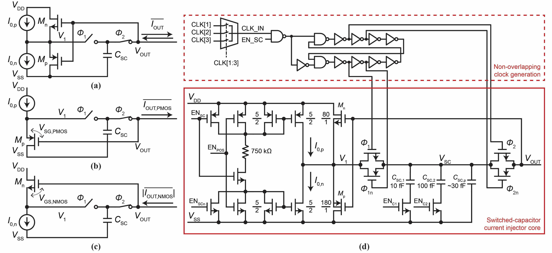
(a) The current injector we implement. (b) With I0,p on and I0,n off, part (a) is reduced to what is shown here, capable of positive current injection. (c) With I0,n on and I0,p off, part (a) is reduced to what is shown here, capable of negative current injection. (d) Transistor-level schematic of the current injector including the non-overlapping clock generation circuit. Control signals CLK[1:3], ENSC, ENPOS, ENC1, and ENC2 are controlled by the pixel’s transparent latch memory.
The bottom of Fig. 7d (solid red box) shows the transistor-level schematic of Fig. 7a. The core switched capacitor circuit uses two transmission gates and can add 10 or 100 fF to the parasitic capacitance CSC,p ∼ 30 fF of the VSC node for CSC. We remove the body effect of transistors Mn and Mp to minimize the |VSG| dependency on VOUT by tying the source and body nodes in both the PMOS and NMOS transistors (the 0.18-☐m technology we use is a triple-well process). A control signal, ENPOS, in the bias network enables either the I0,p or I0,n current sources of Fig. 7a for positive or negative injection. The clock can be selected from three clock inputs, CLK[1:3], and this enables flexible control of fSC across the 4,096 pixels.
D. Clock-Sampling Synchronization
As the current injector in the pCC configuration utilizes switched capacitances, fSC is synchronized to the pixel multiplexer to minimize aliasing of switching induced noise, ∆VOUT of Eq. (6), in the recorded amplifier output signal, Vamp. The aliased ∆VOUT amplitude dominates the noise of the pCC configuration and is larger than any parasitic charge injection or clock feedthrough as it is directly related to the discharging of the switched capacitor into the current injector’s output node/input of the amplifier. To start, Vamp is sampled by a 128:1 output multiplexer (Fig. 3a, c) operated at a frequency of fs ∼ 1.2 MHz resulting in a pixel sample frequency, fs,pixel = fs/128 ∼ 9.4 kHz. To synchronize fSC to fs,pixel across all 128 pixels in the multiplexer, fSC should be an integer multiple of fs,pixel ( fSC = nf s,pixel, n = 1, 2, …) while fs should be an integer multiple of fSC ( fs = mf SC = 128 fs,pixel, m = 1, 2, …). Taken together (n · m = 128), fSC must be a power of 2 multiple of fs,pixel to eliminate aliasing ( fsc = 2N fs,pixel, N = 0, 1, 2, …).
However, this constraint limits the resolution of injected current as . To elaborate, the minimum at fs,pixel ∼ 9.4 kHz would result in available of only 150 pA, 300 pA, 600 pA, 1.2 nA, 2.4 nA, etc. To obtain a higher resolution in the injected current, a non-symmetric clocking scheme is used for generation of fSC (Fig. 8). Effective single integer multiples are established by spacing n pulses as evenly as possible with 1/ fs resolution throughout the total multiplexer period of 1/ fs,pixel = 128/ fs (Fig. 8a). The resultant digital bit stream is then repeated at 128/ fs (equivalent to 1/ fs,pixel, ∼100 μs) to form a continuous output. The current resolution used for experiments is then n·150 pA, n = 1, 2, …, 64. The non-symmetrical switching can increase ∆VOUT by up to 50% at n = 63 (Fig. 8b), yet the synchronization minimizes this increase from affecting signal measurement. A dedicated microprocessor is used to generate the non-symmetric clocks (CLK[1:3] in Fig. 7). During experiments (Section VI.A.) we observe low frequency ∆VOUT noise most likely due to clock drift between the microprocessor and acquisition electronics.
Fig. 8.
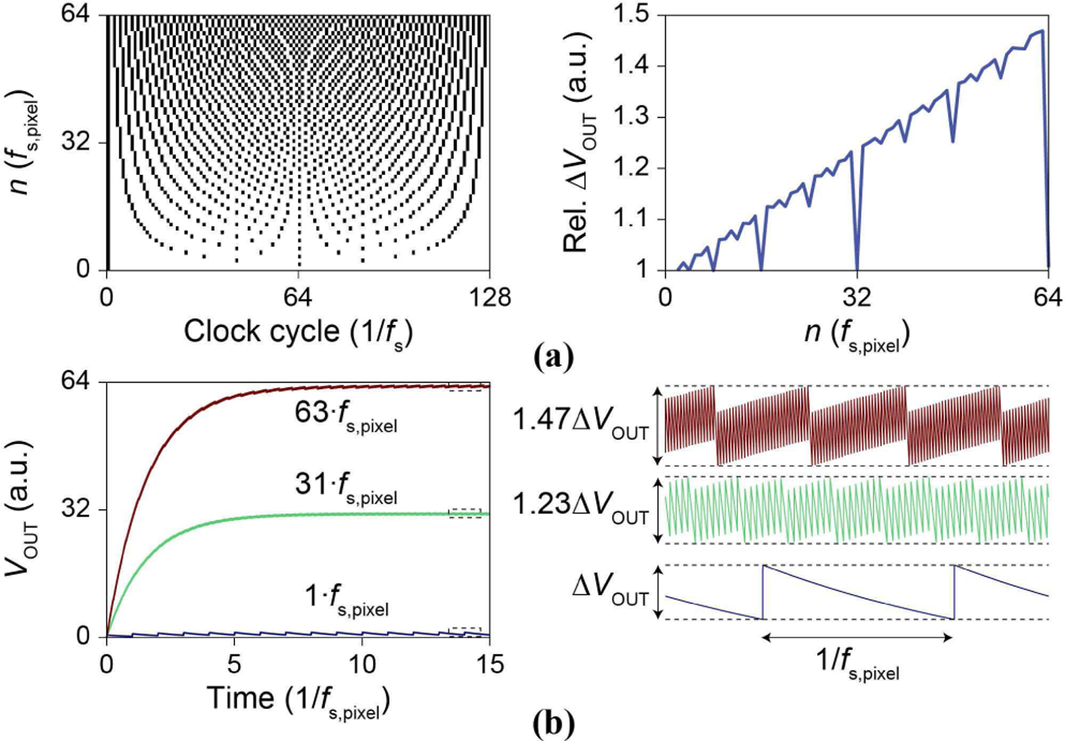
(a, left) pCC clocking scheme to synchronize the switched-capacitor current injector’s fsc to the multiplexer sampling at fs. Black indicates fsc high, white indicates fss low. The clock sequence is repeated after 128/fs . (right) ∆VOUT is increased due to the scheme. (b) Simulated VOUT traces for positive current injection for three different magnitudes and their steady state VOUT(t) ripple voltage.
The same synchronization scheme is used for the pVC configuration, whose transimpedance amplifier also uses a switched capacitance. In this case, we commonly set fTIA = 4 fs,pixel = 37.6 kHz to minimize switching noise.
V. Electrical Characterization
A. Experimental Setup
The IC is packaged and placed on a printed circuit board (PCB) (Fig. 9). The IC and PCB are programmed and read through three National Instruments PXIe-6358 data acquisition (DAQ) cards and interfaced to a computer through LabVIEW software. For digital programming, each pixel is addressed in a shift register (4,096 bits) with real time adjustment/latching of the bit lines (B[1:25] in Fig. 3). For recording, the 4,096 pixel amplifier outputs are divided into 32 subgroups. Each subgroup contains 128 outputs from 2 rows of the array, feeding its own 128:1 analog output multiplexer on chip. Each of the 32× distributed in-pixel multiplexers, shown in Fig. 3c, right, consumes 0.45 mW of total power. 32 NMOS source followers, each consuming 6.86 mW, are then used to buffer the 32× 128:1 multiplexer outputs from the IC to 32× 16 bit analog-to-digital converters of the DAQ cards. Adjacent pixel-to-pixel cross talk within the multiplexer was measured at −43 dB. The overall data rate of recording is 77 MBps.
Fig. 9.
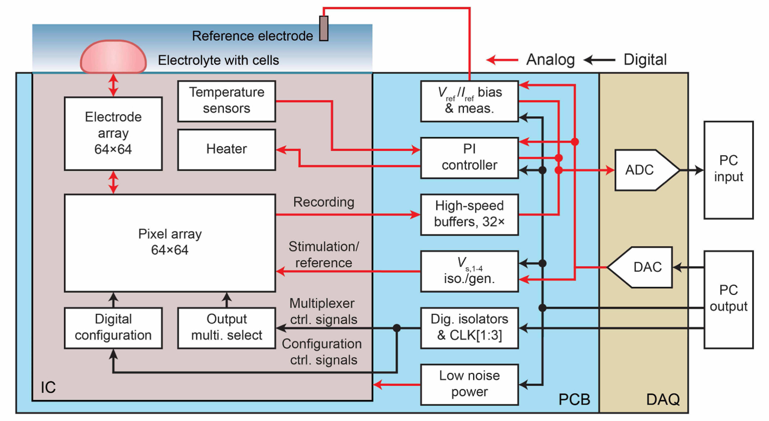
System architecture of the IC and external electronics showing analog and digital signal flow.
The IC’s VSS is set to earth ground and VDD = 3.6 V; this is set higher than the 3.3 V transistors we use, in order to increase both output and stimulation voltage ranges. The Vs,1 to Vs,4 nodes are connected to DAQ analog outputs, which are low pass filtered ( f−3dB ∼ 1 Hz) to provide bias voltages or buffered with a bandwidth of ∼100 kHz to provide voltage signals for various pixel circuit characterizations. The extracellular solution is biased using a Pt or Ag/AgCl reference electrode at Vref , which is adjustable from 0 V to 3.6 V. To regulate the temperature for cell health, the two temperature sensor signals from the IC are fed to an analog PI controller on the PCB, which then sets the voltage of a regulator on the PCB to drive the integrated heater. The designed accuracy for the temperature regulation is <1°C and is calibrated using a thermocouple placed on the surface of the device in solution. In addition to the IC’s total power dissipation of 1.25 W when the array is fully enabled, the heater typically dissipates 0.55 ∼ 0.85 W to maintain 35 °C (Table I). This extra power dissipation is needed to overcome heat loss of the solution on top of the device to the ambient environment and contrasts with MEAs designed for interfacing to thermally insulating tissues or environments. Like the integrated pixel array, the PCB is designed to be highly configurable to ensure ample experimental flexibility and is adjusted using analog switches digitally controlled through a serial interface.
TABLE I.
Power Consumption of the CMOS Device
| Circuit | Power/Circuit |
|---|---|
| Operational amplifier (x4096) | 225 μW |
| Current injector (x4096) | 24 μW |
| Output multiplexer (x32) | 7.3 mW |
| Fully enabled array power consumption | 1.25 W |
| Maximum heater power | 1.3 W |
| Typical heater power to maintain 35°C | 0.55 – 0.85 W |
B. Measurement of Pixel Current Injector
We first characterize the pixel current injector by connecting VOUT to the PCB via Vs,3, bypassing the pixel electrode and the solution. Fig. 10a shows the measured positive and negative vs. fSC (1 kHz ∼ 10 MHz) for VOUT = Vs,3 = 1.8 V (VDD = 3.6 V, VSS = 0 V). They confirm the linear response of to fSC over the 4 decades of frequency, from which we extract VSG,PMOS = 0.63 V, VGS,NMOS = 0.56 V, and CSC,p = 26 fF. The minimum is ∼15 pA at fSC = 1 kHz and the maximum is ∼0.7 μA at fSC = 10 MHz.
Fig. 10.
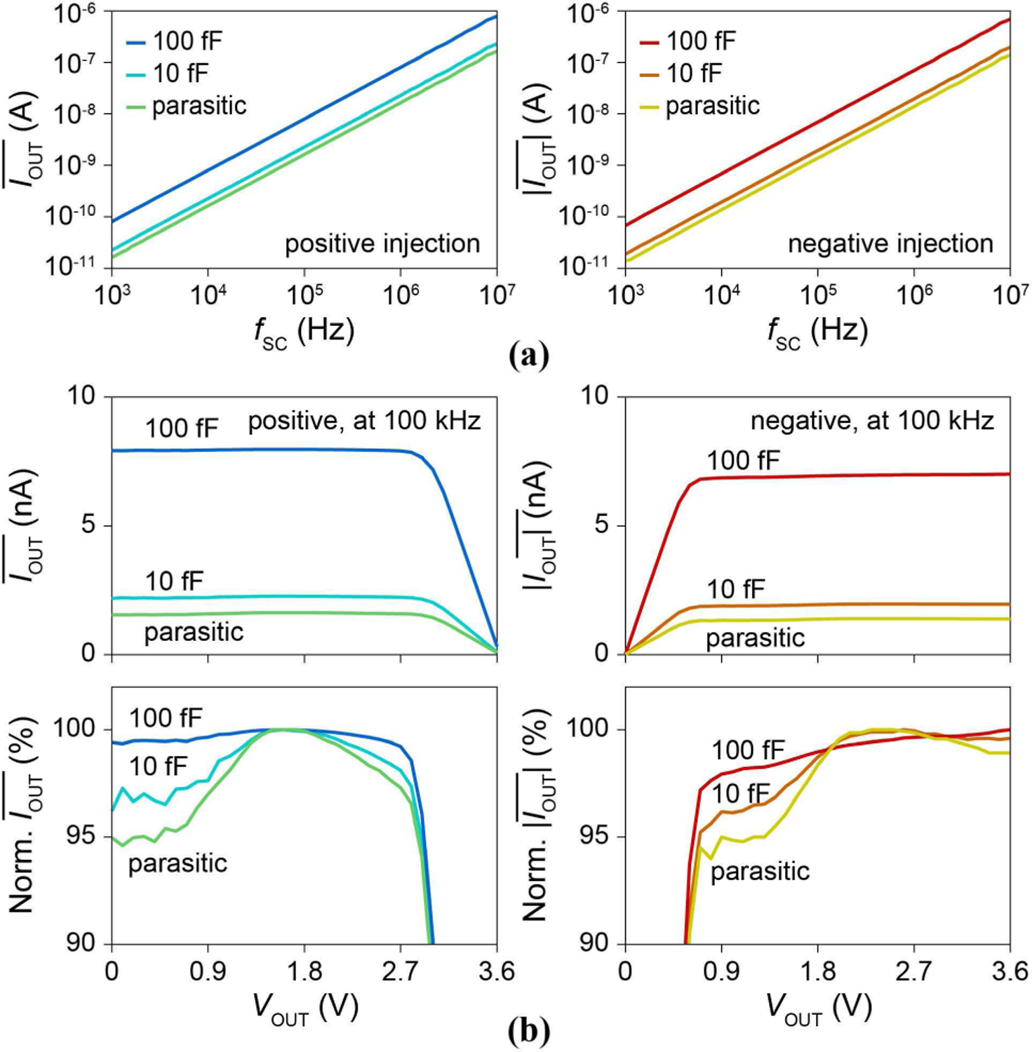
(a) Positive and negative vs. fSC for VOUT = 1.8 V. (b) Positive and negative vs. VOUT for fSC = 100 kHz.
To demonstrate the weak dependence of on VOUT, VOUT = Vs,3 is swept from 0 V to 3.6 V while fixing fSC at 100 kHz. Both currents show flat responses (Fig. 10b), with the positive rolling off around VDD-VSG,PMOS ∼ 3.0 V and the negative rolling off around VSS + VGS,PMOS ∼ 0.6 V. The measured variations of in the flat regions are only within ∼5 % for CSC = CSC,p. Its deviation from theoretical 0.3% is due mainly to the voltage dependence of CSC,p (for CSC = 100 fF + CSC,p where the CSC,p effect is weaker, the current variation is reduced to <2 %). In addition, this variation of for the VOUT sweep remains the same regardless of because ZOUT is approximately inversely proportional to [Eq. (5)]. The discrete negative injection levels for the clock-sampling synchronization scheme (Sec. IV-D) were then measured using CSC = CSC,p, the configuration used for the pCC intracellular measurements. For the pixel shown in Fig. 11, left, is at distinct multiples of −147 pA, corresponding to nf s,pixel. At n = 8, shows <5% variation around ∼ −1.2 nA across the array.
Fig. 11.
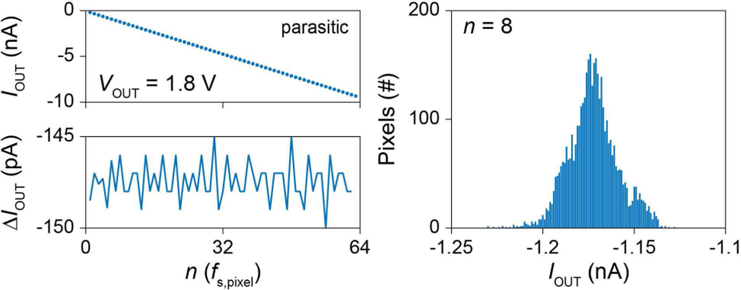
(left) IOUT vs. n of the pCC clock synchronization scheme. (right) Distribution of IOUT at n = 8 for all 4,096 pixels, bin size of 1 pA.
To measure the output ripple voltage ∆VOUT [Eq. (6)] and to highlight the ability for small amplitude current injection, the current injector was tested in solution using a small, 2 μm diameter Pt electrode (with no PtB deposition) post fabricated on the pixel pad (e.g., Fig. 15, top right). This post fabrication involves photolithography to define the hole, dry etching of the foundry passivation to expose the Al pad, deposition of 20 nm Ti and 200 nm Pt, and lift-off [31]. The pixel op-amp was configured as a buffer to measure the voltage ripple during the current injection. We increase fSC from 0 Hz to 1 kHz and then decrease it back to 0 Hz, all in 200 Hz increments (Fig. 12, bottom). This results in ∼5 pA step current increases/decreases for positive/negative injections (Fig. 12, top). The ripple voltage can be clearly seen (Fig. 12, middle at fSC = 600 Hz), with ∼20 mV step size for both positive and negative injections. This ripple voltage for the 2 μm diameter Pt electrode with CL = 1.7 pF is much larger (est. 50×) than the ripple voltage for the PtB electrode that has a much larger CL due to its rough surface texture that increases its surface area. These time-dependent behaviors of and VOUT are consistent with the theoretical considerations of Sec. IV-B (Fig. 6).
Fig. 15.
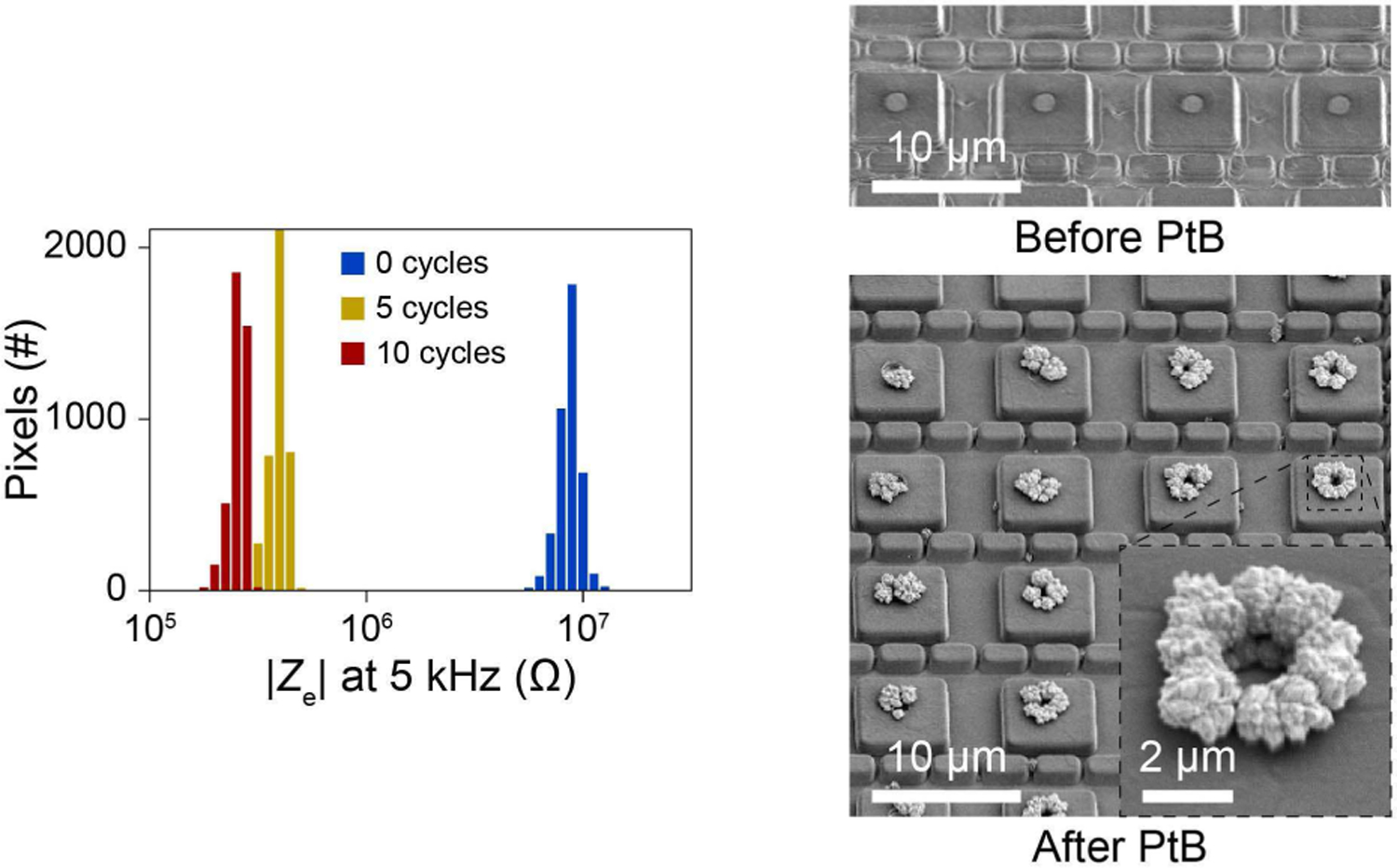
(left) |Ze| at 5 kHz measured across the array during PtB deposition. (right) SEM images of planar hole electrodes before and after PtB deposition.
Fig. 12.
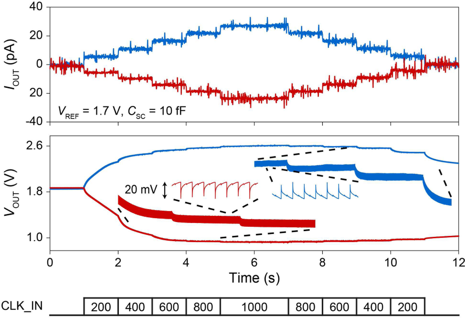
Small amplitude current injection measurement in solution with a post-fabricated Pt electrode. An Ag/AgCl reference was used at VREF = 1.7 V to set VOUT to ∼1.8 V. The insets show the ripple voltage of VOUT for fSC = 600 Hz.
C. Measurement of pCC and pVC Amplifiers
The pCC amplifier configuration was first tested to investigate the optimal number of feedback dps for voltage amplification: the input (Vs,1) output (Vamp) DC transfer curve was measured for each of the 0 to 7 dps options across the array (Fig. 13a). This test is important to ensure array-wide operation: leakage currents across the multiple feedback dps can induce offset voltages that can saturate the amplifier, reducing the number of available pixels. Sharp transitions of the array wide median Vamp,DC from the lower (0.2 V) to upper (2.8 V) output voltage rails for increasing the number of feedback dps show their sensitivity to the leakage currents (Fig. 13a, right). To overcome this sensitivity, not only do we choose the optimal number of feedback dps but we also use the dp connected to Vs,4 to set a current across the feedback dps to tune their offset and impedance.
Fig. 13.
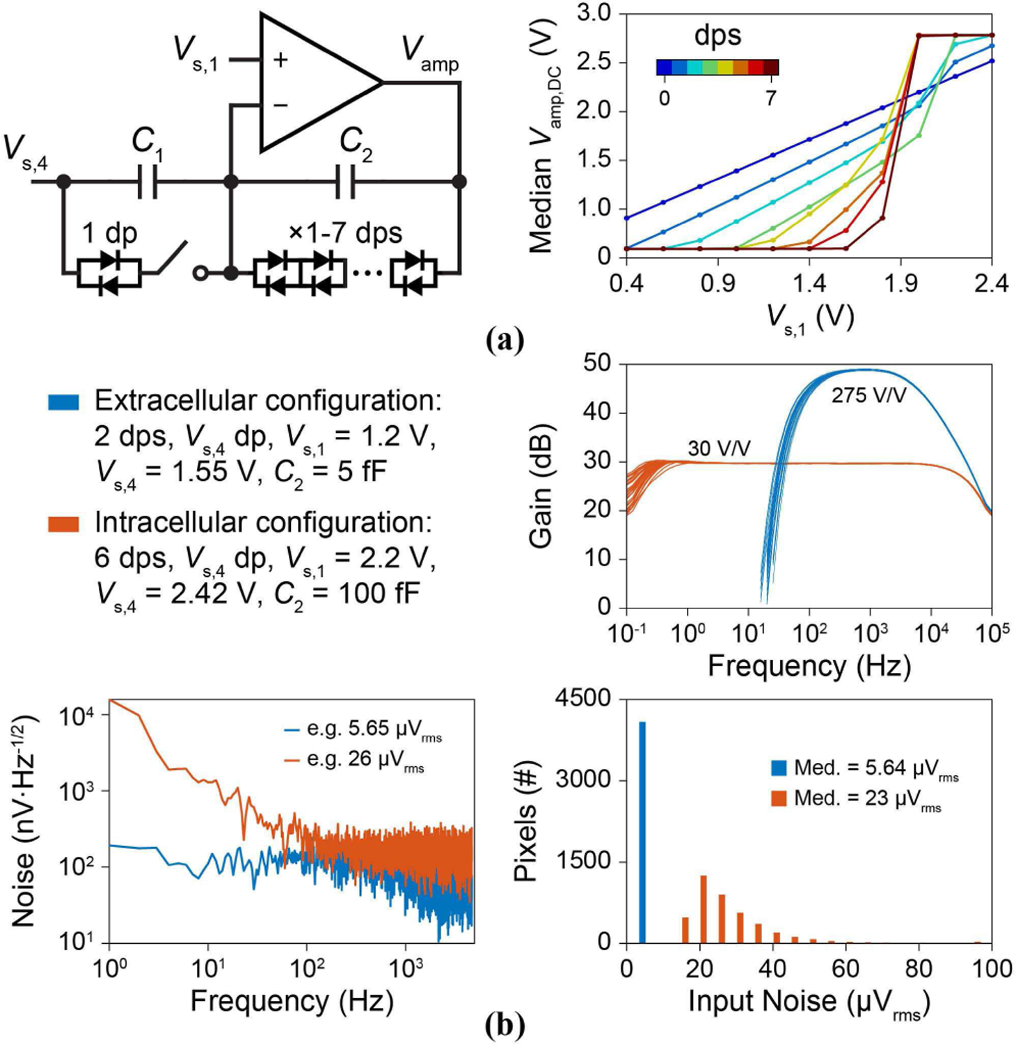
pCC amplifier characterization. (a) The array’s median Vamp,DC vs. Vs,1 for each of the 1-to-7 feedback dp options (without the Vs,4 dp). (b) Measurements of the extracellular and intracellular configurations: gain vs. frequency for 32 pixels, input referred noise for a single example pixel, and input referred noise integrated from 1 Hz to 4.7 kHz across the array.
For the extracellular recording of the membrane potential (this is done later in Section VI by setting Ie = 0 in the pCC configuration so as not to cause membrane permeabilization), we use 2 feedback dps in parallel to C2 = 5 fF to set a passband gain of 275 V/V with a bandwidth f1 = 100 Hz to f2 = 5 kHz (Fig. 13b). The 100-Hz pole substantially filters out the 1/ f noise, given that the open-loop amplifier has a 1/ f noise corner of ∼10 Hz. The measured input referred noise is 5.6 μVrms when integrated from 1 Hz to 4.7 kHz (Fig. 13b).
The pCC intracellular recording mode (done later in Section VI with non-zero Ie) must deal with larger amplitude signals (∆Ve > 1 mV or ∆Vamp > 300 mV). In this case, since the 2 feedback dps exhibit non-linear clipping, we instead use 6 feedback dps to lessen the voltage seen on each dp with large output voltages. In this configuration, the feedback current is especially essential to control Vamp,DC across the array that would otherwise be saturated due to the sharp slope observed in Fig. 13a with 6 dps. With this measure, signals as large as ∆Ve > 20 mV can be recorded without distortion. On the other hand, the large impedance of the 6 dps causes f1 < 1 Hz; this lets in a larger amount of 1/ f noise (as the open-loop amplifier has the 1/ f corner at ∼10 Hz), resulting in an increased integrated input referred noise of ∼23 μVrms at Av = 30 V/V (Fig. 13b). Digital filters can reduce this additional low frequency noise depending upon the signal frequencies of interest (e.g., PSPs range from ∼100 Hz to 1 kHz).
Figure 14 shows the characterization of the pVC transimpedance amplifier. Input current, Iin, is applied using Vs,4 through C1 = 3.5 pF (Fig. 14a, left) to measure the transimpedance gain RTIA ∼ 700 MΩ for fSC,pVC = 4 fs,pixel = 37.6 kHz and for Vs,1 = 1.0 V ∼ 2.4 V (Fig. 14a, right). The bandwidth of the transimpedance amplifier extends from DC to 2 kHz set by RTIA and C2 = 100 fF (Fig. 14b, left) with an input referred noise as low as 1.1 pArms integrated from 1 Hz to 4.7 kHz (Fig. 14b, right). Gain and noise measurements across the array show a distinct spatial dependency due to multiplexer sampling and its relation to the clock phases (Fig. 14c): pixels which are sampled during Φ1 exhibit larger noise and gain in comparison to Φ2. These variations could be optimized in future designs by incorporating a dedicated switched feedback element synched to the multiplexer in the pixel circuit and using a traditional integrate and reset method for the lowest noise performance [35].
Fig. 14.
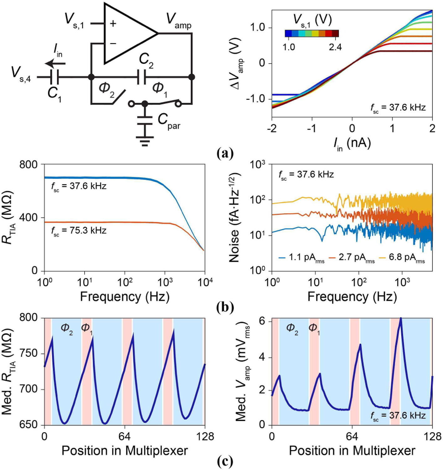
(a, left) pVC transimpedance amplifier measurement setup. (right) Measured transimpedance with 2.5-ms Iin pulse inputs (Vs,1: 1.0 ∼ 2.4 V). (b, left) Transimpedance gain, RTIA vs. frequency for 32 pixels for fSC,pVC = 37.6 kHz and 75.3 kHz. (right) Input referred current noise for 3 pixels. (c) Median RTIA and Vamp voltage noise of 128 pixels sharing an output multiplexer.
D. Characterization of Electrode and Routing Capacitance
For optimal pCC and pVC coupling [Eqs. (1)–(4)], we desire a small electrode impedance (Ze) or a large electrode capacitance Ce. Concretely: is the condition to obtain the final expression in Eq. (1), eliminating the attenuation due to the electrode; and , is the condition to obtain the final expressions of Eqs. (3) and (4) with no attenuation due to the electrode. To minimize Ze (i.e., to increase Ce), PtB is electrodeposited onto Pt electrodes post fabricated on the Al pads, as the surface roughness of PtB increases the electrode surface area (e.g., Fig. 15, right) [31]. For the PtB deposition, Vs,1 is used to apply a voltage ramp to Ve from 0 V to −1.2 V at 50 mV/s with respect to a Pt reference in a solution of 0.5 mM H2PtCl6 and 25 mM NaNO3 [36]. Ze is measured across the array periodically throughout the deposition by applying a 1–25 mV 5 kHz sine wave sequentially to each pixel and measuring the resultant current through the reference electrode (Fig. 15, left). Ze is reduced by almost 2 orders: e.g., in Fig. 15, it is reduced to ∼300 kΩ (Ce ∼ 100 pF).
This Ce satisfies for the final expression of Eq. (1) to hold, with C1 ∼ 3.5 pF and Cp,r ∼ 600 fF - 2 pF, depending on the routing length. We extract this Cp,r by comparing the amplifier gain measured from Vs,1 to Vamp with C1 connected to Vs,4 at ground and the same gain but with C1 connected to Ve (Fig. 16). Also for Eqs. (3) and (4) is satisfied with Rs and Rjm in the MΩ range. The electrode-to-electrode coupling was also measured in a similar manner by applying a 1-V AC signal to all Ve but the pixel measured: a total of 3.0 fF of electrode-to-electrode capacitance was measured, of which, 2.3 fF was due to adjacent electrode pads while 0.7 fF was from pixel circuit to electrode routing cross-coupling capacitance.
Fig. 16.
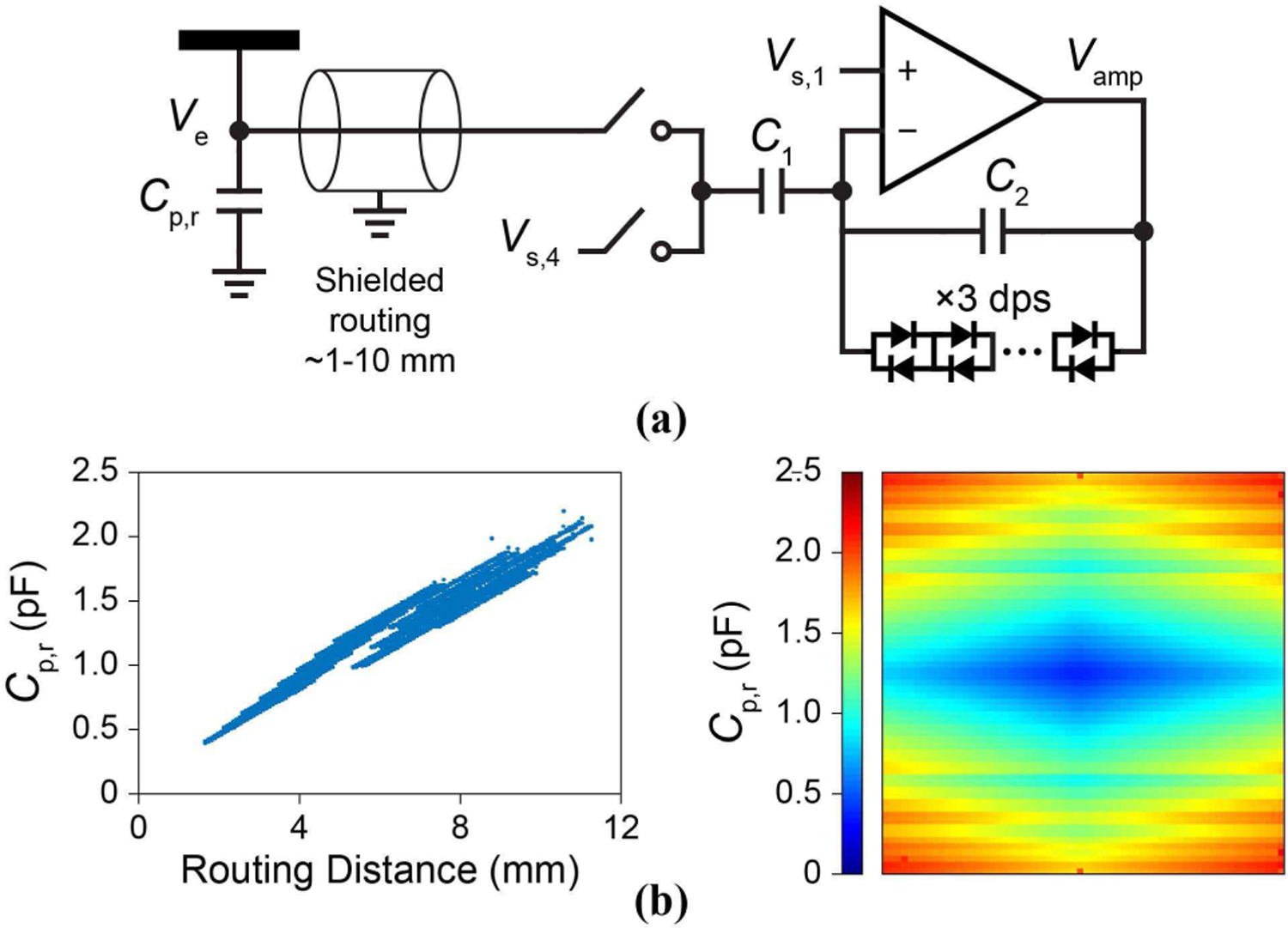
(a) The configuration for measurement of Cp,r. (b, left) Dependence of Cp,r on the electrode pixel routing distance. (right) Heat map across the array.
Beyond reducing Ze, the surface roughness of the PtB also strongly interacts with the cell membrane to form a tight seal [31], increasing Rs. This not only further ensures for Eqs. (3) and (4) to be valid for the pVC operation, but also reduces the attenuation of the pCC recording [Eq. (1)] and enhances the pCC stimulation effectiveness [Eq. (2)].
VI. Electrophysiological Measurements
We demonstrate pCC and pVC intracellular recording and stimulation with dissociated rat neurons, cultured on the IC for 10–14 days in vitro. We use PtB vertical nanoneedles for pVC and PtB vertical nanoneedles with pad edge electrodes for pCC [31]. Fig. 17 shows an example extracellular signals recorded using the high-gain, low-noise voltage amplifier configuration of our CMOS IC—-similar to other CMOS MEAs [1], [2], [11]–[14], [3]–[10]—-as a reference for comparison to the intracellularly recorded signals we will present now.
Fig. 17.
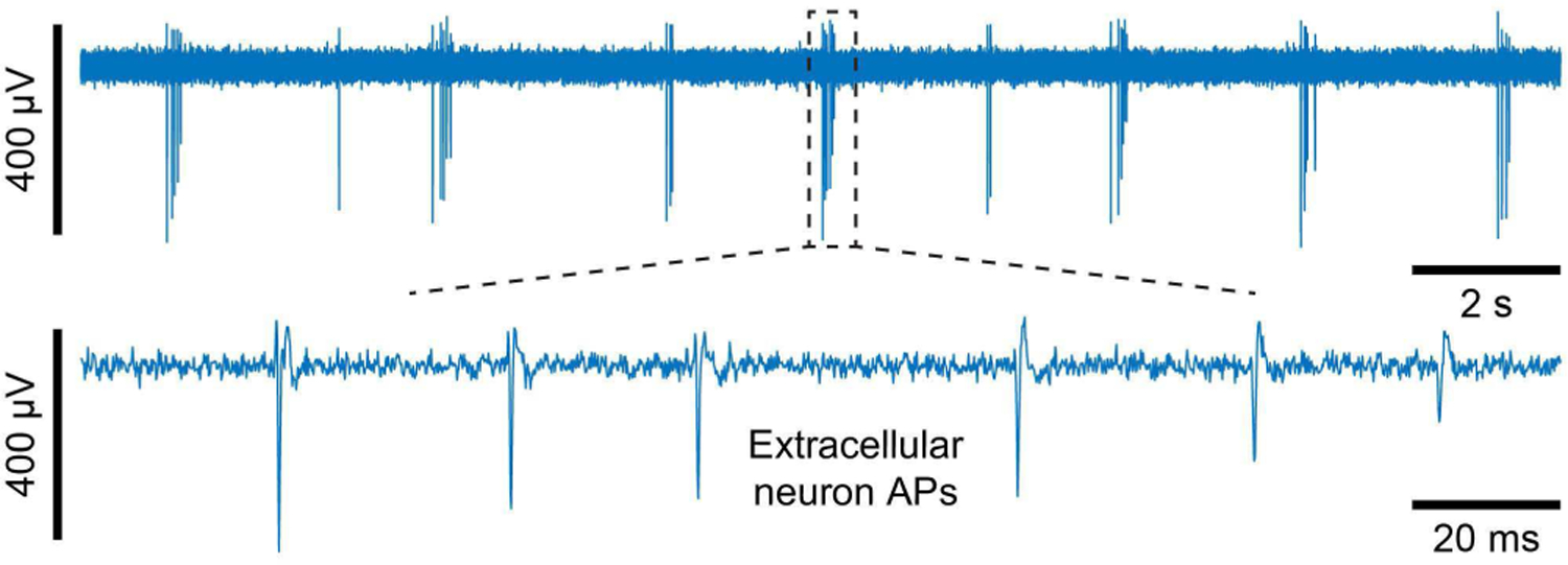
Example of extracellular recording of a dissociated rat neuron using a PtB planar hole electrode.
A. pCC Neuron Measurements
To demonstrate the pCC operation, we first determined the threshold Ie needed for intracellular access by changing Ie from 0 ∼ −3.0 nA with a step of −150 pA and measuring Ve with the rat neurons on top (Fig. 18a). The threshold Ie was determined when Ve substantially increased and APs were clearly distinguished (Fig. 18a). The intracellular threshold so determined lied between −1.1 to −2.2 nA across the array.
Fig. 18.
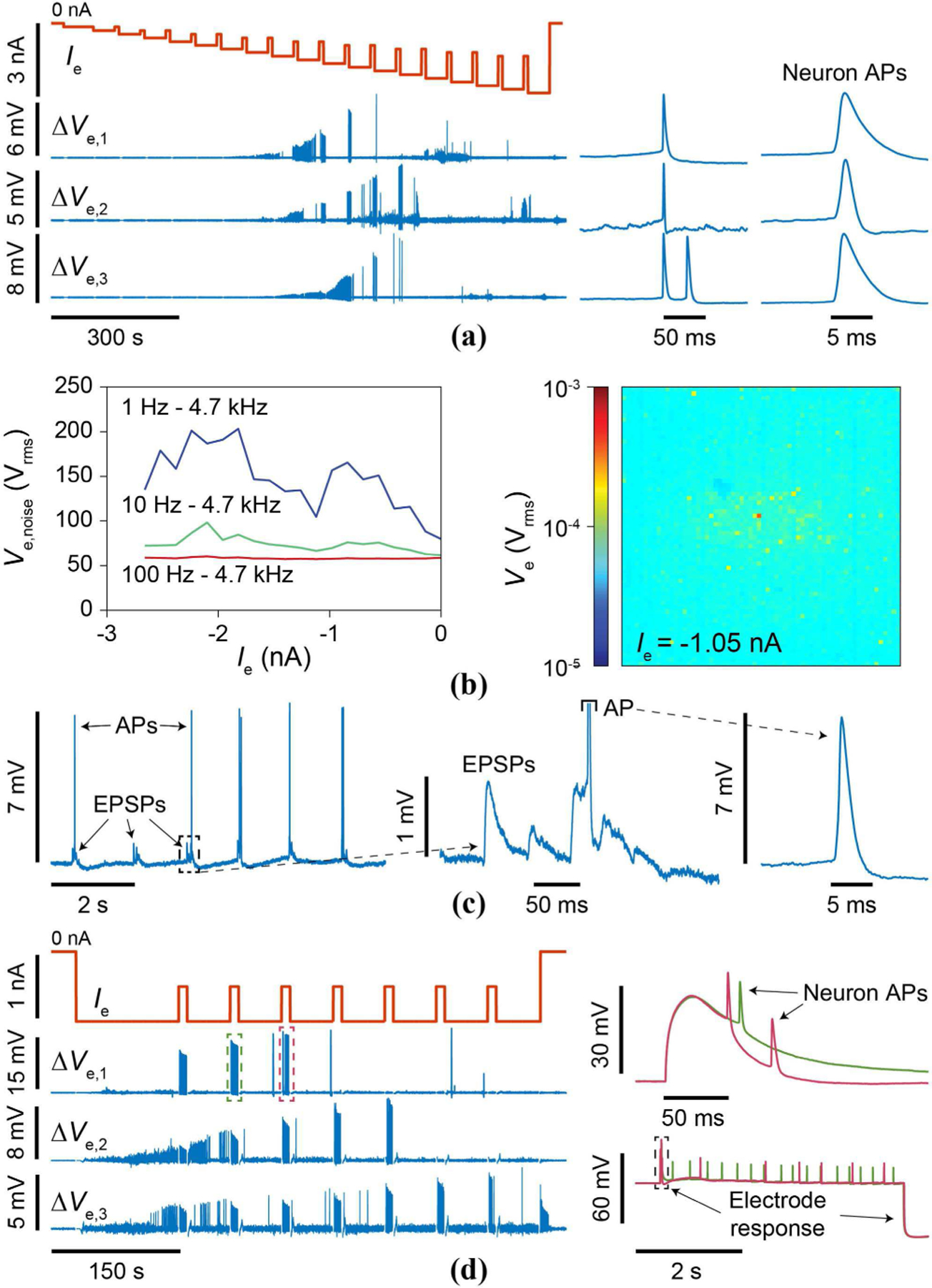
(a) Ramped experiment to determine intracellular threshold Ie with dissociated rat neurons. (b) Integrated Ve,noise for an individual pixel without an interfacing neuron (left) and Ve amplitude integrated from 100 Hz - 4.7 kHz across the array below threshold for the experiment of (a). (c) Excitatory PSP (EPSP) measurement. (d) Stimulation is achieved through adjustment of Ie.
To quantify the overall noise at the electrode beyond the input referred noise of the pCC amplifier, we performed two types of experiments. First, we measured Ve for various bandwidths again by changing Ie from 0 ∼ −3.0 nA, but this time without a neuron above (Fig. 18b, left shows the data for an example pixel). Second, we measured Ve with the Ie below the intracellular threshold so that no intracellular coupling occurs even if there is a neuron above (Fig. 18b, right shows the data across the array). These experiments show that on top of the ∼23 μVrms input referred noise of the pCC intracellular-mode amplifier (Section V. C), there is an additional noise of 40 ∼ 150 μVrms largely below 10 Hz in frequency. This extra noise originates from the electrode (∼10 μVrms), solution (∼30 μVrms [12]), and the current injector’s ripple voltage (0 ∼ 110 μVrms, dependent upon |Ie|). If the clock of the switched-capacitor current injector and that of the output multiplexer were perfectly synchronized, the ripple voltage noise would disappear in its entirety (Section IV. D), but in reality, the two clocks slightly drift from each other at low frequencies below 10 Hz, which aliases the ripple voltage into the recording noise at the low frequencies. The non-uniformity of the noise across the array (Fig. 18b, right) is attributed to variations in f1 arising from feedback diode leakage current variation. By comparing this overall noise to the AP amplitudes of 1 ∼ 30 mV measured at the electrode in the pCC intracellular mode (e.g., Fig. 18a, right), we obtain a signal-to-noise ratio > 20, on par with the patch clamp. The signal-to-noise ratio for PSPs is also > 1, so subthreshold (synaptic) signal measurement is also possible. An example of such subthreshold sensitivity is shown in Fig. 18c, where excitatory PSPs (EPSPs) are clearly measured with ∆Ve amplitudes of ∼200 μV to ∼1 mV at the electrode.
A stimulation experiment with intracellular coupling at Ie ∼ −1.1 nA with periodic +550 pA injections (Fig. 18d), during which increased neuron AP firings are observed, demonstrates the ability to intracellularly record ∆Ve and adjust Ie simultaneously to stimulate the neuron through the same electrode.
The scalability of the device for network-wide intracellular recording was demonstrated with intracellular measurement of more than 1,700 neurons in parallel for a > 40% intracellular coupling rate [31]. The subthreshold sensitivity enabled cross-pixel AP to PSP correlation that allowed mapping of 304 synapses between 396 neurons, which demonstrates the capability of the IC for synaptic connectivity mapping applications [31].
B. pVC Neuron Measurements
To demonstrate the pVC operation, we gradually increased the magnitude of Ve to determine the threshold for intracellular access (Fig. 19). Since no spontaneous activity is observed for pVC due to its low input impedance, voltage stimulations were applied to activate the neuron’s ion channels: at Ve = −0.65 V to −0.7 V distinct Na+ spikes and K+ repolarization currents are observed during stimulation, clearly distinguished in the high-pass (100 Hz) filtered version of the measured electrode current, ∆Ie. The pVC mode clearly enables the ability to measure Ie and adjust Ve simultaneously, allowing for concurrent intracellular recording of ion channel currents and stimulation of membrane potentials.
Fig. 19.
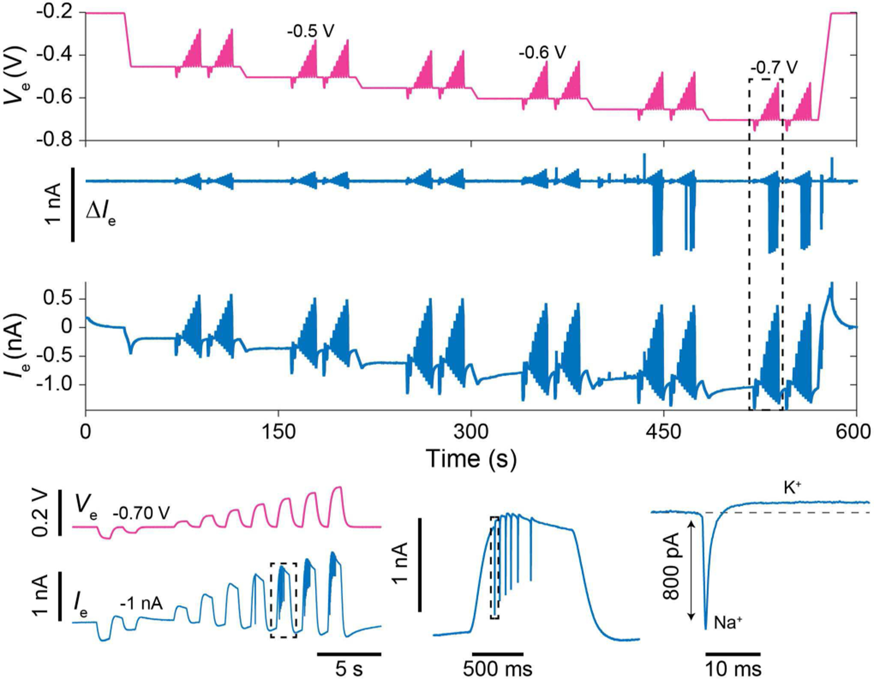
Ramped Ve experiments in the pVC configuration to determine threshold for intracellular access using a PtB nanoneedle electrode and dissociated rat neurons. Ve stimulations are applied to activate ion channels.
Such intracellular ion-channel measurement of mammalian neurons can be useful for high-throughput drug screening applications, where current high-throughput intracellular tools, i.e., the planar patch clamp, are limited to non-neuronal, artificial cell lines. As a first demonstration towards this end, we measured the effects of ion-channel drugs affecting both the Na+ and K+ currents of the dissociated rat neurons [31].
VII. Conclusion
We have presented the CMOS IC that contains 4,096 pCC/pVC pixel circuits, with each connected to a PtB electrode. The electrodes form a dense, 20 μm pitch 64 × 64 array. Overall the IC enables large-scale intracellular recording of neurons with the ability of simultaneous excitations. It is the flexibility of the pixel circuit, containing a new switched-capacitor based current injector and a highly configurable op-amp, that enables both the pCC and pVC modes within each pixel circuit. The lateral separation of the pixel circuit from electrode decouples the electrode pitch from the larger pixel circuit area for the low noise design with the high configurability. The device has been fabricated in 0.18 μm CMOS technology, electrically characterized, and verified biologically with in vitro rat neurons. We summarize and compare the performance of this CMOS nanoelectrode array to start-of-the-art CMOS MEAs as well as our prior CMOS nanoelectrode array in Table II [3]–[6], [14], [25].
TABLE II.
Performance Comparison of State-of-the-Art CMOS Micro and Nano Electrode Arrays
| [3] | [4], [14] | [5] | [6] | [25] (Our prior work) |
This work | ||
|---|---|---|---|---|---|---|---|
| Technology node | 0.18 μm | 0.18 μm | 0.13 μm | 0.13 μm | 0.35 μm | 0.18 μm | |
| Electrode shape | Planar microelectrode with surface roughness | Planar microelectrode | Planar microelectrode | Planar microelectrode | Vertical nanoelectrode | Vertical nanoelectrode with surface roughness | |
| Electrode pitch | 13.5 μm | 25.5 μm | 58 μm | 15 μm | 126 μm | 20 μm | |
| No. electrodes | 59,760 | 65,536 | 1,024 | 16,384 | 1,024 | 4,096 | |
| No. recording channels | 2,048 | 65,536 | 4 | 1,024 | 1,024 | 4,096 | |
| Cell-electrode interface modality | Extracellular voltage recording | Yes | Yes | Yes | Yes | Yes | Yes |
| Intracellular voltage recording with no concurrent stimulation | - | - | - | Yes (cardiomyocyte) |
Yes (cardiomyocyte) |
Yes (cardiomyocyte) |
|
| Intracellular voltage recording with current injection (current clamp) | - | - | - | - | - | Yes (neuron) |
|
| Intracellular current recording with voltage application (voltage clamp) | - | - | - | - | - | Yes (neuron) |
|
| Constant voltage stimulation (CVS) | Yes | Yes | - | Yes | Yes | Yes | |
| Constant current stimulation (CCS) | Yes | - | Yes | Yes | - | Yes | |
| Impedance monitoring | - | - | - | Yes | - | - | |
| Impedance spectroscopy | Yes | - | Yes | Yes | - | - | |
| Chemical | Yes | - | - | - | - | - | |
| No. stimulation waveform generation units | 16 (V or I) | External (V) | 4(I) | 64 (V) + 64 (I) | External (V) | External (V) + 4,096 (I) | |
| No. stimulation waveforms | 6 (V or I) | 1(V) | 4(I) | 64 (V) + 64 (I) | 3 (V) | 3 (V) + 3 (I) | |
| No. sites for simultaneous CVS | N/A | 65,536 | - | 4,096 | 1,024 | 4,096 | |
| No. sites for simultaneous CCS | 6 | - | 4 | 64 | - | 4,096 | |
| CVS/CCS range | ±1.5 V/±300 μA | 3.3 V/- | - / ± 32 μA | ± 1.65 V/± 382.5 nA | 4 V/ - | 3 V / ± 300 μA | |
| CVS/CCS resolution (LSB) | 2.9 mV/ 29 nA | N/A | 250 nA | 103 mV/2 pA | - | - /5pA (140 pA for PCC) | |
| Channel gain | 30–7000 | 50–250 | 22–412 | 2–3000 | 150–375 | 30–275 | |
| Channel bandwidth (maximum) | 1 Hz- 10kHz | 100 Hz – 10 kHz | 0.1 Hz-26 kHz | 0.5 Hz −10 kHz, | 1 Hz-5kHz | <1 Hz to 30 kHz | |
| Input-referred noise (rms) | Full band | 5.4 μV | 12.6 μV | 12 μV | 250 μV | 23 μV | |
| AP band | 2.4 μV | 10 μV | 7 μV | 7.5 μV | 5.6 μV | ||
| ADC | 10b @ 20 kS/s | External | External | 10b @ 20 kS/s | External | External | |
| Temperature control | Yes (temp, sensor) |
- | - | - | - | Yes (temp, sensor with heater and external PID controller |
|
| Total power | 86 mW | 153 mW | N/A | 95 mW | 12 mW | 1.25 W (w/o heater) | |
Acknowledgments
This work was supported by Samsung Advanced Institute of Technology, Samsung Electronics under A37734, the Army Research Office under W911NF-15-1-0565 and W911NF-15-1-0548, the National Science Foundation under DGE1745303, the National Institutes of Health under 1-U01-MH105960-01, the Gordon and Betty Moore Foundation, and the Catalyst Foundation of Valhalla, NY.
Biographies

Jeffrey Abbott received the B.S./M.S. degrees in electrical engineering from the Rochester Institute of Technology, Rochester, NY, USA, in 2011 and the Ph.D. degree in engineering sciences from the School of Engineering and Applied Sciences at Harvard Unveristy, Cambridge, MA, USA in 2017. He is currently a postdoctoral fellow in the labs of Prof. Hongkun Park and Prof. Donhee Ham at Harvard University.
His current research interests include analog integrated circuits, applications of nanotechnology to neuroscience, and high-throughput CMOS biosensors.

Tianyang Ye received the B.S. degree in Microelectronics from Peking University, Beijing, China in 2013 and Ph.D. degree from Harvard University, MA, USA in 2020. He is currently doing research as a postdoctoral fellow in Prof. Hongkun Park’s lab in Harvard University.
His current research interests include nanoscience, developing novel nano-bio interfaces, and building high-throughput electrophysiology platforms for ex-vivo systems.

Keith Krenek received B.S./M.S. degrees in electrical engineering from Texas A&M University, College Station, TX, USA, in 2014/2015, and the Ph.D. degree in applied physics from Harvard University, Cambridge, MA, USA in 2019.
His research interests include biosensors and microfluidics, photonic integrated circuits, rapid prototyping applied in new fields, guidance and navigation systems, and ionizing radiation physics.

Ling Qin received the B.S. degree in electrical engineering from Tsinghua University, Beijing, China, in 2000. He received the Ph.D. degree in engineering sciences from the School of Engineering and Applied Sciences at Harvard University, Cambridge, MA, USA, in 2017. He is currently a SerDes design engineer at Apple, Inc.
His current research interests include analog and mixed-signal integrated circuits, high-speed links, sensors, and silicon-cell interface.

Youbin Kim received a B.A. in physics from Harvard University, Cambridge, MA, USA in 2018. He is currently pursuing a Ph.D in electrical engineering at UC Berkeley, Berkeley, CA, USA.
His research interests include digital integrated circuits, computer architecture, and the design of hardware accelerators for high-dimensional computing and machine learning algorithms.

Wenxuan Wu received the B.S. degree in electrical engineering (with minor in chemistry) from University of Washington, WA, USA in 2015. He is currently pursuing the Ph.D. degree in electrical engineering with the School of Engineering and Applied Sciences at Harvard University, MA, USA.
His current research interests include integrated circuit design for neurosciences, mixed signal circuit design, and bio-electronic interface design.

Rona S. Gertner received the B.A. degree in Biochemistry from Brandeis University, Waltham, MA, USA in 1996. She received the M.Sc. degree and the Ph.D. degree in Biology from the Weizmann Institute of Science, Rehovot, Israel in 2001 and 2007, respectively. Since 2009 she has been a Research Assistant in the laboratory of Prof. Hongkun Park of the Department of Chemistry and Chemical Biology at Harvard University, Cambridge, MA, USA.

Hongkun Park received a B.S. degree in chemistry from Seoul National University, Seoul, South Korea, in 1990. He received a Ph.D. degree in chemistry from Stanford University, Stanford, CA, USA, in 1996. He is Mark Hyman Jr. Professor of Chemistry and Professor of Physics at Harvard University.
His current research interests include solid-state quantum optoelectronics, quantum sensing and control, and nano-bio interfacing.

Donhee Ham (SM’12) received the B.S. degree (summa cum laude) in physics from Seoul National University, Seoul, South Korea, in 1996. Following a 1.5 years of military service in the South Korea Army, he went to the California Institute of Technology, Pasadena, CA for graduate training in physics under Barry Barish, and later received the Ph.D. degree in electrical engineering in 2002, winning the Charles Wilts Prize.
He is currently Gordon McKay Professor of Applied Physics and Electrical Engineering at Harvard University and is Fellow of Samsung Electronics. His other work experiences include the Caltech-MIT Laser Interferometer Gravitational Wave Observatory (LIGO), IBM T. J. Watson Research, technical program committees in the IEEE International Solid-State Circuits Conference and the IEEE Asian Solid-State Circuits Conference, advisory board for the IEEE International Symposium on Circuits and Systems, guest editorship for the IEEE Journal of Solid-State Circuits, and associate editor for the IEEE Transactions on Biomedical Circuits and Systems.
His current research focus relevant to this paper is CMOS-bio interfaces for neuroscience, machine intelligence, and biological data archiving.
Contributor Information
Jeffrey Abbott, John A. Paulson School of Engineering and Applied Sciences, the Department of Chemistry and Chemical Biology, and the Department of Physics, Harvard University, Cambridge, MA 02138, USA.
Tianyang Ye, John A. Paulson School of Engineering and Applied Sciences, Harvard University, Cambridge, MA 02138, USA..
Keith Krenek, John A. Paulson School of Engineering and Applied Sciences, Harvard University, Cambridge, MA 02138, USA..
Ling Qin, John A. Paulson School of Engineering and Applied Sciences, Harvard University, Cambridge, MA 02138 USA. He is now with Cavium Inc., Marlborough, MA 01752, USA..
Youbin Kim, Harvard College, Cambridge, MA 02138 USA. He is now with University of California, Berkeley, CA 94720, USA..
Wenxuan Wu, John A. Paulson School of Engineering and Applied Sciences, Harvard University, Cambridge, MA 02138, USA..
Rona S. Gertner, Department of Chemistry and Chemical Biology, Harvard University, Cambridge, MA 02138, USA.
Hongkun Park, Department of Chemistry and Chemical Biology and the Department of Physics, Harvard University, Cambridge, MA 02138 USA..
Donhee Ham, John A. Paulson School of Engineering and Applied Sciences, Harvard University, Cambridge, MA 02138, USA..
References
- [1].Eversmann B et al. , “A 128 × 128 CMOS Biosensor Array for Extracellular Recording of Neural Activity,” IEEE J. Solid-State Circuits, vol. 38, no. 12, pp. 2306–2317, 2003. [Google Scholar]
- [2].Heer F, Hafizovic S, Franks W, Blau A, Ziegler C, and Hierlemann A, “CMOS microelectrode array for bidirectional interaction with neuronal networks,” IEEE J. Solid-State Circuits, vol. 41, pp. 1620–1629, 2006. [Google Scholar]
- [3].Dragas J et al. , “In Vitro Multi-Functional Microelectrode Array Featuring 59 760 Electrodes, 2048 Electrophysiology Channels, Stimulation, Impedance Measurement, and Neurotransmitter Detection Channels,” IEEE J. Solid-State Circuits, vol. 52, no. 6, pp. 1576–1590, Jun. 2017. [DOI] [PMC free article] [PubMed] [Google Scholar]
- [4].Tsai D, Yuste R, and Shepard KL, “Statistically Reconstructed Multiplexing for Very Dense, High-Channel-Count Acquisition Systems,” IEEE Trans. Biomed. Circuits Syst, vol. 12, no. 1, pp. 13–23, 2018. [DOI] [PMC free article] [PubMed] [Google Scholar]
- [5].Park JS et al. , “1024-Pixel CMOS Multimodality Joint Cellular Sensor/Stimulator Array for Real-Time Holistic Cellular Characterization and Cell-Based Drug Screening,” IEEE Trans. Biomed. Circuits Syst, vol. 12, no. 1, pp. 80–94, 2018. [DOI] [PMC free article] [PubMed] [Google Scholar]
- [6].Lopez CM et al. , “A multimodal CMOS MEA for high-throughput intracellular action potential measurements and impedance spectroscopy in drug-screening applications,” IEEE J. Solid-State Circuits, vol. 53, no. 11, pp. 3076–3086, 2018. [Google Scholar]
- [7].Berdondini L et al. , “Active pixel sensor array for high spatio-temporal resolution electrophysiological recordings from single cell to large scale neuronal networks,” Lab Chip, vol. 9, no. 18, p. 2644, 2009. [DOI] [PubMed] [Google Scholar]
- [8].Frey U et al. , “Switch-matrix-based high-density microelectrode array in CMOS technology,” IEEE J. Solid-State Circuits, vol. 45, no. 2, pp. 467–482, 2010. [Google Scholar]
- [9].Livi P, Heer F, Frey U, Bakkum DJ, and Hierlemann A, “Compact voltage and current stimulation buffer for high-density microelectrode arrays,” IEEE Trans. Biomed. Circuits Syst, vol. 4, no. 6 PART 1, pp. 372–378, 2010. [DOI] [PubMed] [Google Scholar]
- [10].Huys R et al. , “Single-cell recording and stimulation with a 16k micro-nail electrode array integrated on a 0.18 μm CMOS chip,” Lab Chip, vol. 12, no. 7, p. 1274, 2012. [DOI] [PubMed] [Google Scholar]
- [11].Ballini M et al. , “A 1024-channel CMOS microelectrode array with 26,400 electrodes for recording and stimulation of electrogenic cells in vitro,” IEEE J. Solid-State Circuits, vol. 49, no. 11, pp. 2705–2719, 2014. [DOI] [PMC free article] [PubMed] [Google Scholar]
- [12].Obien MEJ, Deligkaris K, Bullmann T, Bakkum DJ, and Frey U, “Revealing neuronal function through microelectrode array recordings,” Front. Neurosci, vol. 9, no. January, p. 423, 2015. [DOI] [PMC free article] [PubMed] [Google Scholar]
- [13].Müller J et al. , “High-resolution CMOS MEA platform to study neurons at subcellular, cellular, and network levels,” Lab Chip, vol. 15, no. 13, pp. 2767–2780, 2015. [DOI] [PMC free article] [PubMed] [Google Scholar]
- [14].Tsai D, Sawyer D, Bradd A, Yuste R, and Shepard KL, “A very large-scale microelectrode array for cellular-resolution electrophysiology,” Nat. Commun, vol. 8, no. 1, 2017. [DOI] [PMC free article] [PubMed] [Google Scholar]
- [15].Wagenaar DA, Pine J, and Potter SM, “Effective parameters for stimulation of dissociated cultures using multi-electrode arrays,” J. Neurosci. Methods, vol. 138, no. 1–2, pp. 27–37, September. 2004. [DOI] [PubMed] [Google Scholar]
- [16].Hamill OP, Marty A, Neher E, Sakmann B, and Sigworth FJ, “Improved patch-clamp techniques for high-resolution current recording from cells and cell-free membrane patches,” Pflügers Arch. Eur. J. Physiol, vol. 391, no. 2, pp. 85–100, August. 1981. [DOI] [PubMed] [Google Scholar]
- [17].Verkhratsky A, Krishtal OA, and Petersen OH, “From Galvani to patch clamp: the development of electrophysiology,” Pflügers Arch. - Eur. J. Physiol, vol. 453, no. 3, pp. 233–247, 2006. [DOI] [PubMed] [Google Scholar]
- [18].Perin R, Berger TK, and Markram H, “A synaptic organizing principle for cortical neuronal groups,” Proc. Natl. Acad. Sci, vol. 108, no. 13, pp. 5419–5424, March. 2011. [DOI] [PMC free article] [PubMed] [Google Scholar]
- [19].Duan X et al. , “Intracellular recordings of action potentials by an extracellular nanoscale field-effect transistor,” Nat. Nanotechnol, vol. 7, no. 3, pp. 174–179, 2011. [DOI] [PMC free article] [PubMed] [Google Scholar]
- [20].Xie C, Lin Z, Hanson L, Cui Y, and Cui B, “Intracellular recording of action potentials by nanopillar electroporation,” Nat. Nanotechnol, vol. 7, no. 3, pp. 185–190, 2012. [DOI] [PMC free article] [PubMed] [Google Scholar]
- [21].Hai A and Spira ME, “On-chip electroporation, membrane repair dynamics and transient in-cell recordings by arrays of gold mushroom-shaped microelectrodes,” Lab Chip, vol. 12, no. 16, pp. 2865–2873, 2012. [DOI] [PubMed] [Google Scholar]
- [22].Shmoel N, Rabieh N, Ojovan SM, Erez H, Maydan E, and Spira ME, “Multisite electrophysiological recordings by self-assembled loose-patch-like junctions between cultured hippocampal neurons and mushroom-shaped microelectrodes,” Sci. Rep, vol. 6, 2016. [DOI] [PMC free article] [PubMed] [Google Scholar]
- [23].Robinson JT, Jorgolli M, Shalek AK, Yoon M-H, Gertner RS, and Park H, “Vertical nanowire electrode arrays as a scalable platform for intracellular interfacing to neuronal circuits,” Nat. Nanotechnol, vol. 7, no. 3, pp. 180–184, 2012. [DOI] [PMC free article] [PubMed] [Google Scholar]
- [24].Lin ZC, Xie C, Osakada Y, Cui Y, and Cui B, “Iridium oxide nanotube electrodes for sensitive and prolonged intracellular measurement of action potentials,” Nat. Commun, vol. 5, 2014. [DOI] [PMC free article] [PubMed] [Google Scholar]
- [25].Abbott J et al. , “CMOS nanoelectrode array for all-electrical intracellular electrophysiological imaging,” Nat. Nanotechnol, vol. 12, no. 5, pp. 460–466, February. 2017. [DOI] [PubMed] [Google Scholar]
- [26].Dipalo M et al. , “Intracellular and Extracellular Recording of Spontaneous Action Potentials in Mammalian Neurons and Cardiac Cells with 3D Plasmonic Nanoelectrodes,” Nano Lett, vol. 17, no. 6, pp. 3932–3939, June. 2017. [DOI] [PMC free article] [PubMed] [Google Scholar]
- [27].Liu R et al. , “High Density Individually Addressable Nanowire Arrays Record Intracellular Activity from Primary Rodent and Human Stem Cell Derived Neurons,” Nano Lett, vol. 17, no. 5, pp. 2757–2764, May 2017. [DOI] [PMC free article] [PubMed] [Google Scholar]
- [28].Braeken D et al. , “Open-cell recording of action potentials using active electrode arrays,” Lab Chip, vol. 12, no. 21, p. 4397, 2012. [DOI] [PubMed] [Google Scholar]
- [29].Dipalo M et al. , “Plasmonic meta-electrodes allow intracellular recordings at network level on high-density CMOS-multi-electrode arrays,” Nat. Nanotechnol, vol. 13, no. 10, pp. 965–971, 2018. [DOI] [PubMed] [Google Scholar]
- [30].Abbott J, Ye T, Ham D, and Park H, “Optimizing Nanoelectrode Arrays for Scalable Intracellular Electrophysiology,” Acc. Chem. Res, vol. 51, no. 3, pp. 600–608, February. 2018. [DOI] [PubMed] [Google Scholar]
- [31].Abbott J et al. , “A nanoelectrode array for obtaining intracellular recordings from thousands of connected neurons,” Nat. Biomed. Eng, vol. 4, no. 2, pp. 232–241, February. 2020. [DOI] [PMC free article] [PubMed] [Google Scholar]
- [32].De Dorigo D et al. , “Fully immersible subcortical neural probes with modular architecture and a delta-sigma ADC integrated under each electrode for parallel readout of 144 recording sites,” IEEE J. Solid-State Circuits, vol. 53, no. 11, pp. 3111–3125, November. 2018. [Google Scholar]
- [33].Harrison RR and Charles C, “A low-power low-noise CMOS amplifier for neural recording applications,” IEEE J. Solid-State Circuits, vol. 38, no. 6, pp. 958–965, 2003. [Google Scholar]
- [34].Spira ME and Hai A, “Multi-electrode array technologies for neuroscience and cardiology,” Nat. Nanotechnol, vol. 8, no. 2, pp. 83–94, 2013. [DOI] [PubMed] [Google Scholar]
- [35].Crescentini M, Bennati M, Carminati M, and Tartagni M, “Noise limits of CMOS current interfaces for biosensors: A review,” IEEE Trans. Biomed. Circuits Syst, vol. 8, no. 2, pp. 278–292, April. 2014. [DOI] [PubMed] [Google Scholar]
- [36].Li L-L, Chang C-W, Wu H-H, Shiu J-W, Wu P-T, and Wei-Guang Diau E, “Morphological control of platinum nanostructures for highly efficient dye-sensitized solar cells,” J. Mater. Chem, vol. 22, no. 13, p. 6267, 2012. [Google Scholar]


