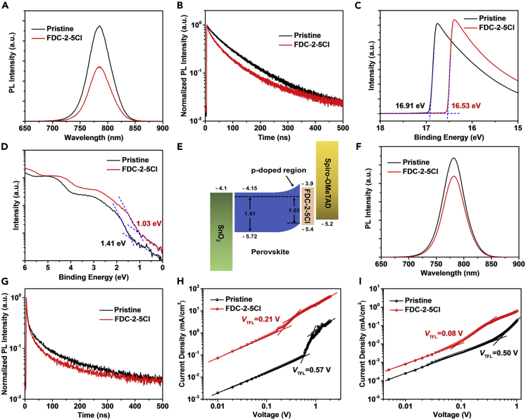
Figure 2.
Characterizations of carrier lifetime, charge transfer, and trap density of perovskite film
(A and B) (A) PL and (B) TR-PL spectra of perovskite films without and with FDC-2-5Cl treatment. UPS spectra of perovskite films with and without FDC-2-5Cl treatment.
(C and D) (C) The secondary electron cutoff region and (D) the frontier electronic structure region.
(E) Illustration of proposed energy band bending at the surface of the perovskite due to the charge transfer from perovskite to FDC-2-5Cl.
(F and G) (F) PL and (G) TR-PL spectra of perovskite/spiro-OMeTAD films without and with FDC-2-5Cl treatment.
(H and I) The dark J-V characteristics of devices with structure of (H) glass/ITO/SnO2/perovskite/PCBM/Ag and (I) glass/ITO/NiO/perovskite/spiro-OMeTAD/Ag.

