

Abstract
The use of non-ideal reflective materials and low-precision manual manufacturing technologies is a fundamental technical obstacle blocking the positron emission tomography (PET) systems from achieving better performances. We propose to address that long-standing obstacle with advanced multilayer dielectric coating technologies. We designed an broad-band multilayer high-reflectivity (HR) film that can be coated directly on the surface of ultra-precision polished lutetiumyttrium oxyorthosilicate (LYSO) scintillators. The film consists of 48 layers of TiO2/SiO2/HfO2 which are deposited on LYSO scintillator crystal alternately using the electron beam evaporation method. The overall thickness of the HR film is about 3μm. The HR film combines 3 quarter wavelength reflective films, with the central wavelengths of 365 nm, 430 nm and 570 nm respectively, to match the emission spectrum of the LYSO scintillator. The optical experimental results show that the HR film achieved an excellent average reflectivity of 99.50% at 8° incident angle for incident lights with wavelengths between 360 to 620 nm. The average reflectivity at 60° incident angle is higher than 90%. The results of the hardness experiments and the adhesive strength experiments show that the HR film has an excellent mechanical strength. The HR coating technology developed in this study is very attractive because it allows to “print” high-performance reflectors on a scintillator directly with high-precision, instead of manually gluing reflective films on the scintillator. Thus, we conclude that the HR film provides a viable solution to the long standing technical bottleneck that limits the development of high-performance detectors for advanced PET imaging.
Keywords: Mirror coating; Detector design and construction technologies and materials; Gamma detectors (scintillators, CZT, HPG, HgI etc); Optics
1. Introduction
Positron Emission Tomography (PET) became commercially available many years ago with successful applications in cardiology, neurology and oncology [1–3]. The overall performance of a PET system is largely determined by the performance of the detector module, in terms of discrete crystal decoding [4], depth of interaction (DOI) decoding [5, 6], energy resolution [7], timing resolution [8, 9] and intrinsic sensitivity [10]. Many factors have an impact on the performance of the PET detector, such as the properties of the scintillator crystal [11, 12], the optical properties of the light guides and coupling materials, the surface treatment of the scintillator crystals and light guides, the optical reflectance properties of the reflectors [13], the pattern and depth of the slots in the light guide (for PMT-based block detectors) and the performance of the photon detectors [14].
The choice of optical reflector impacts the detector module performance. The commonly-used optical reflectors are ESR films, Lumirror films, Teflon tapes, Tyvek papers and titanium dioxide paint [15, 16]. The typical reflection coefficient and thickness of the most commonly used ESR films are 98.5% and 65–70 μm, respectively. In detector modules for sub-millimeter preclinical PET imaging, the thickness of the reflector is the critical limitation of the detector module’s fill factor and sensitivity [17]. For example, a high-resolution imager constructed with sub-millimeter scintillator crystals was constructed with detectors using crystals 0.5 mm × 0.5 mm in size and 0.1 mm-thick reflectors. The fill factor of the detector was only 64%, and the resulting detector sensitivity was very low. The sensitivity of this detector would be improved by 38% by using an broad-band reflector with a thickness of 30 μm.
Detector performance is also determined by the manufacturing precision when constructing the detector. Poor precision leads to degradation of the detector performance and mismatches between the simulations/designs and actual measurements. It is difficult to develop a new generation of high-performance detector module, because it depends on so many factors. The design of PET detector modules depends heavily on the designers’ experience and intuition and is largely based on trial and error, which is costly, time-consuming, and inefficient. PET detector modules designed this way generally do not have optimized performance. Researchers need to design and construct enough high-quality detector modules to build their prototype cameras, which takes considerable time and effort.
The use of non-ideal reflective materials and low-precision manual manufacturing technologies is a fundamental technical obstacle blocking the PET systems from achieving better performances. We propose to address that fundamental technical obstacle with advanced multilayer dielectric coating technologies. HR coating is very attractive because it allows to “print” high-performance reflectors on a scintillator directly with high-precision, instead of manually gluing reflective films on the scintillator. Dielectric multilayer film is commonly used to build high reflectivity reflectors [18, 19]. It is constructed by alternately depositing thin layers of materials such as magnesium fluoride, calcium fluoride and various metal oxides on the optical substrate [20, 21]. By choosing the exact composition and the optimized film parameters including the thickness and number of these layers, it is possible to tailor the reflectivity of the film to produce the desired optical characteristic.
In this study, we designed a high-reflectivity, HR film with 48 layers of HfO2/SiO2/TiO2 to match the entire emission spectrum of cerium doped lutetium-yttrium oxyorthosilicate scintillator (Lu21–xY2xSiO5:Ce, LYSO:Ce), which had high output with improved energy resolution, short decay time and excellent radiation hardness [22–24]. The LYSO samples were processed using high-precision polishing techniques and coated with the HR films using electron beam evaporation techniques. The optical and mechanical properties of the HR film, including reflection spectrums, nanohardness and film-substrate interfacial adhesion strength were tested. The scope of this paper is to describe the design and fabrication of the 48-layer HR coating and to evaluate its performance in terms of optic and mechanical properties. The paper is organized as follows: in section 2, the HR film design, the surface finish and the method of HR film fabrication are introduced. The experimental settings to assess the HR films are given in details. In section 3, the experimental results are presented. In section 4 and 5, the main features of the 48-layer HR coating technologies are summarized and discussed.
2. Materials and methods
2.1. Simulation-based HR film design
Two essential guidelines have been followed in designing the HR film coating on the LYSO. The first one is to match the reflectance spectrum of the film with the emission spectrum of LYSO which ranges from 360 nm to 620 nm [25] with the central emission wavelength at 420 nm. The second one is to maximize the reflectance of the film at wavelengths across the whole emission spectrum of LYSO.
The most commonly-used dielectric coating materials include Fluoride (CaF2, MgF2, Na3 AlF6 and etc.), Sulfide (ZnS and etc.), and Oxide (TiO2, Ta2O5, ZrO2, HfO2, and MgO). In this study, we selected three dielectric materials (HfO2, SiO2 and TiO2) because they have low absorption coefficients, stable and suitable refractive indexes, high chemical stability, high bulk density, high adhesion strength, low film stress and good material uniformity. The indexes of refraction of TiO2, SiO2 and HfO2 are 2.2~2.4, 1.46 and 1.92~2 (370 nm ~ 420 nm) respectively.
Typical dielectric high reflective film consists of a stack of 1/4 wavelength films, which is prepared by depositing alternately two different materials with high and low refractive index [26]. However, the simulation-based design study shown that a single HR film constructed with two different materials was not able to cover the whole emission spectrum of LYSO (360 nm ~ 620 nm). Thus, we combined three layers of quarter wavelength reflective films to match the emission spectrum of the LYSO scintillator. The three layers of films are two films of TiO2/SiO2 with the central wavelengths of 570 nm and 435 nm respectively, and a film of HfO2/SiO2 with the central wavelength of 355 nm.
Before design the coating film, three LYSO samples (4 mm × 4 mm × 20 mm) were manufactured, polished and tested with a spectroscopic ellipsometer to experimentally characterize the refractive index of LYSO. In addition, we have also measured the transmittance of a polished LYSO sample 4 mm in thickness with a UV/Vis Spectrophotometer (LAMBDA™, PerkinElmer). The measured refractive indexes were imported into Essential Macleod that is a professional optical coatings design software for accurate film simulation and design. Simulated Annealing method was applied to vary the thickness, number of layers and central wavelengths of the film to minimize the reflectance of the coating film across the entire emission spectrum of LYSO.
2.2. Surface finish
The roughness of surface finish is an essential parameter that affects the optical properties of the reflection (specular and/or diffuse reflection, and reflectance), uniformity and accuracy of the film thickness, and mechanical strength of film. In practice, the polished surfaces with specular reflection are more preferable in a detector module constructed with a monolithic scintillator crystal [27–31], while the rough surfaces with diffuse reflection are more desirable in a detector module constructed with array of discrete scintillator crystals [13]. Technically, it is more challenging to design and implement coating on a rough surface uniformly, accurately and with well-controlled mechanical strengths. Thus, we chose to polish the LYSO crystals and coat them with films of specular reflection in this study.
Six thin LYSO slices (20 mm × 30 mm × 1 mm), and twenty LYSO cuboids (5 mm × 6 mm × 30 mm) were manufactured for coating. All samples were polished using polyurethane polishing pad and CeO2 polishing solution (particle size of 1μm). The macro and micro surface roughness were measured by 3D optical surface profilers (ZYGO New View) and atomic force microscopy (AFM, SPM9700) respectively.
2.3. HR film fabrication
A pilot experiment was firstly performed to validate the coating technologies before apply them on the LYSO samples. Three layers of Ta2O5/SiO2/Ta2O5 was deposited on a silicon substrate using electron beam evaporation method. The quality of the coating, in terms of accuracy and uniformity, was assessed by imaging the cross-section of the film with a scanning electron microscope (SEM, Nova NanoSEM 450).
The polished LYSO samples with the designed HR film, both the LYSO samples and the dielectric materials (99.9% purity) were heated to 300°C to remove the moistures and impurity from the substances. In the film deposition process, oxygen gas (99% purity) was inputted into the deposition chamber to compensate the loss of oxygen atom from the TiO2 particles, which would lead to an increase in high photon absorption rate and a decrease in the reflectivity. The designed multilayer film structure was fabricated by depositing the three dielectric materials (HfO2, SiO2 and TiO2) alternately with a 5×10⁻³Pa background pressure and a 2×10⁻²Pa working pressure.
2.4. Performance characterization
The performance of the film was measured in terms of coating accuracy and uniformity, reflectance, and mechanical strength. Two coated thin slices (20 mm × 30 mm × 1 mm) were sectioned and the cross-sections were scanned with a scanning electron microscope (SEM) to assess the accuracy and uniformity of the coating. In addition, three coated thin slices were scanned with AFM to assess the micro surface roughness of the film. The reflectance spectrums of the coated LYSO samples at five different incident angles (0°, 8°, 15°, 45° and 60°) were characterized using the absolute reflectance measurements method with LAMBDA 750 UV/Vis/NIR Spectrophotometer (PerkinElmer). The measurements were made in room temperature (21.5°C) and with a humidity of 59%.
Two experiments were performed to assess the mechanical strengths of the films. The nanohardness and nanoindentation of the films were measured with Hysitron TI750 using Berkovich tip (three-sided pyramid tip, total included angle of 142.3°). The interfacial adhesion in the film-LYSO structure was characterized with a scarification instrument using Rockwell tip (conical indenter, radius of curvature and taper angle of the tip were 100μm and 120° respectively [32]).
3. Results
3.1. Simulation-based HR film design
Figure 1 (a) shows the reflective index of the LYSO samples at the wavelengths range from 200 nm to 1500 nm. The measured reflective index ranged from 1.85 to 1.80 across the emission spectrum of LYSO (360 nm to 620 nm) and was 1.83 at the central emission wavelength (420 nm). Figure 1 (b) shows the transmittance of LYSO measured from the sample 4 mm in thickness. A transmittance of 90.47% was measured at the 420 nm central emission wavelength. However, the transmittance surprisingly dropped to 50% at 380 nm wavelength.
Figure 1.
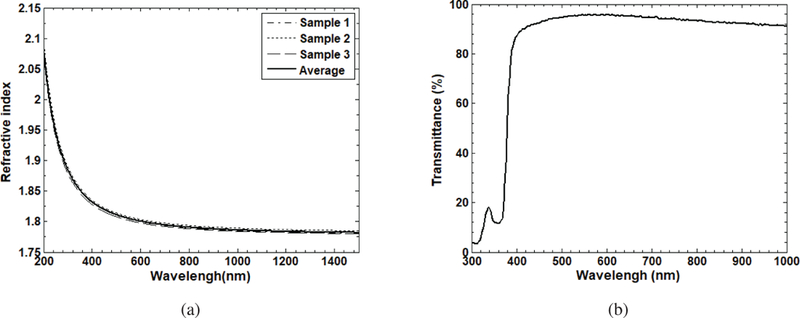
(a) The refractive index of LYSO. Three samples (20 mm × 30 mm × 1 mm in size) were measured. The average of the three measurements are represented by the solid curve. (b) The transmittance of a 4 mm thick LYSO sample.
The simulation-based HR film was performed with the measured refractive indexes using Simulated Annealing method. The optimized HR film structure (with reference wavelength = 455nm) is LYSO[1.25(H1L)8][(H1L)7][0.78(H2L)9]Air. Here, H1, L, H2 stand for TiO2, SiO2 and HfO2 respectively. The HR film had 48 layers, which formed the three quarter-wavelength reflective components with the central wavelengths of 365 nm, 455 nm and 570 nm to match the entire emission spectrum of LYSO scintillator. Table 1 shows the details of the 48-layer HR film structure and the deposition rate of different materials in HR film fabrication. The overall thickness of the HR film is 3033.7 nm. The theoretic spectral reflectance curve of the 48-layer HR film at normal incidence is shown in figure 2. The reflectance at 360 nm, 420 nm, and 620 nm are 98.56%, 99.74% and 97.03% respectively. The average reflectance over the emission spectrum of LYSO (360 nm to 620 nm) is 99.42%.
Table 1.
Parameters of HR film structure and deposition parameter.
| Quarter Wavelength Multilayer |
Number of Layer |
Materials | Thickness (nm) |
Deposition rate (Å/s) |
|---|---|---|---|---|
| TiO2/SiO2 @570 nm | 1 | TiO2 | 62.9 | 4 |
| 2 | SiO2 | 98 | 15 | |
| ...... | ...... | ...... | ...... | |
| 15 | TiO2 | 62.9 | 4 | |
| 16 | SiO2 | 98 | 15 | |
| TiO2/SiO2 @455 nm | 17 | TiO2 | 46.5 | 4 |
| 18 | SiO2 | 72.5 | 15 | |
| ...... | ...... | ...... | ...... | |
| 29 | TiO2 | 46.5 | 4 | |
| 30 | SiO2 | 72.5 | 15 | |
| HfO2/SiO2 @355 nm | 31 | HfO2 | 43.2 | 5 |
| 32 | SiO2 | 58.3 | 15 | |
| ...... | ...... | ...... | ...... | |
| 47 | HfO2 | 43.2 | 5 | |
| 48 | SiO2 | 58.3 | 15 | |
Figure 2.

The theoretic spectral reflectance of the 48-layer HR film at normal incidence.
3.2. Surface finish
Figure 3 (a) shows four polished samples. All samples have excellent light-admitting quality and have no visible cracks or other defects. Figure 3 (b) and (c) show a typical ZYGO image measured on an area of 264 μm × 353 μm, and a typical AFM image measured on an area of 5 nm x 5 nm. The macro and micro Ra surface roughness (arithmetical mean deviation) of polished LYSO samples calculated from the ZYGO image and the AFM image were 0.57 nm and 0.89 nm respectively. Both numbers are smaller than the central emission wavelength (420 nm) of the LYSO.
Figure 3.
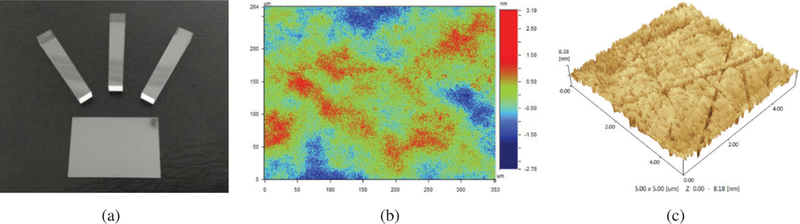
(a) The polished LYSO samples. The large sample is 20mm × 30mm × 1 mm in size. The small one is 5 mm × 6 mm × 30mm in size. (b) The ZYGO image of a polished crystal surface. (c) The AFM image of a polished crystal surface.
3.3. HR film fabrication
Figure 4 (a) shows the SEM image of the cross section of the tri-layer film (Ta2O5/SiO2/Ta2O5) coated on a Silicon substrate using electron beam evaporation method. The thickness of the three layers are 66.4 nm, 168.2 nm and 46.3 nm respectively. While the mechanical cutting has caused some damages on the top Ta2O5 layer, the layers below are excellently flat, smooth and uniform. Figure 4 (b), (c) and (d) show the AFM surface maps of the first layer (Ta2O5), the second layer (SiO2) and the third layer (Ta2O5) of the tri-layer film, respectively. The micro Ra surface roughness of three layers calculated from the three AFM images were 0.724 nm, 0.860 nm and 1.249 nm, respectively. These Ra numbers are smaller than the minimum thickness (43.2 nm) of the individual layers of the 48-layer HR film (table 1). Thus, we conclude that the electron beam evaporation method is capable of producing high-quality coatings that fulfil our requirements.
Figure 4.

(a) The SEM image of the cross section of the tri-layer film on a Silicon substrate. The AFM surface mapping of (b) the first layer (Ta2O5), (c) the second layer (SiO2) and (d) the third layer (Ta2O5) of the tri-layer film.
3.4. Performance characterization
Figure 5 (a) shows the picture of one uncoated sample and two coated samples. The reflection of background letters (“ABABAB”) on the coated samples are clear, while the reflection on the uncoated sample is hardly readable. Figure 5 (b) shows the pictures of an ESR film, a coated JGS1 fused Silica, a coated LYSO sample and a coated K9 glass slide. The differences of the reflections among the samples are no detectable by visual inspection.
Figure 5.
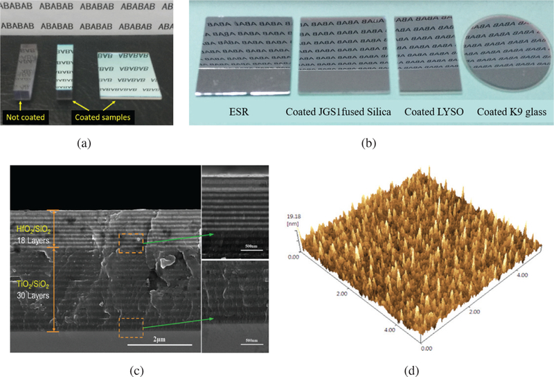
(a) Picture of an uncoated sample and two coated samples. (b) Pictures of an ESR file, a coated JGS1 fused Silica, a coated LYSO sample and a coated K9 glass slide. (c) SEM image of the cross-section of the 48-layer dielectric film on a LYSO substrate. (d) The AFM image of the HR film surface.
Figure 5 (c) shows a SEM image of the cross-section of the 48-layer dielectric film on the LYSO substrate. While the mechanical cutting has caused some visible damages on the cross-section, the 18 layers of HfO2/SiO2, 30 layers of TiO2/SiO2and the interfaces between the layers are generally clear, flat, smooth and uniform. Figure 5 (d) shows the AFM surface map of 48-layer film. The micro Ra surface roughness calculated from the AFM image was 1.936 nm. The uniform and high coating quality shown in figure 5 (c) and (d) indicates a uniform reflectance over the surface of the coated samples.
Figure 6 (a) shows the measured reflectance spectrums of a coated LYSO samples at five different incident angles (0°, 8°, 15°, 45° and 60°). The average reflectivity at 0°, 8°, 15°, 45° and 60° incident angles for incident lights with wavelengths between 360 to 620nm are 98.06%, 99.65%, 99.00%, 97.02% and 89.93%, respectively. The reflectivity at 0°, 8°, 15°, 45° and 60° incident angles for incident lights with the central emission wavelength (420nm) are 98.94%, 99.87%, 99.58%, 98.87% and 97.10%, respectively. The HR films had excellent reflectance as expected. Figure 6 (b) compares the simulated and the measured reflectance spectrums at the 0° incident angle. The experimental results agree with the simulation results well.
Figure 6.

(a) The measured reflectance spectrum of the HR film deposited on LYSO samples. The incident angles are 0°, 8°, 15°, 45° and 60° respectively. (b) Comparison of the simulated and the measured reflectance spectrums at the 0° incident angle.
The results of the nanohardness and nanoindentation tests are shown in figure 7. The shape of the Berkovich tip (three-sided pyramid tip, total included angle of 142.3°) are clearly identical in the surface image of indentation (figure 7 a). The profile analysis (figure 7 b) shows that there is no pile-up [33] around the edges of indentation. Figure 7 (c) and (d) show the nanohardness and the elastic modulus measured at different depths of indentation. Those results show that the film has excellent mechanical properties in terms of nanohardness and elastic modulus.
Figure 7.
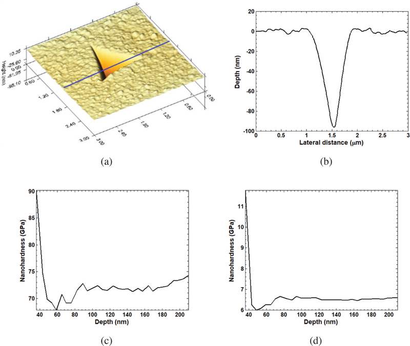
(a) The surface image of indentation with maximum indentation depth set at 215 nm. (b) The profile of indentation at the position marked by the blue line in (a). (c) The nanohardness and (d) the elastic modulus measured at different depths of indentation.
In the interfacial adhesion strength experiments, a Rockwell tip was used to scratch the film. A linearly incremental loading force was applied on the tip while it moved/scratched on the surface of the HR coated samples. The loading force, the friction and the scratching sound were recorded simultaneously during the experiments. Figure 8 shows typical experimental results. Three scratching sound signals (marked as A, B and C in figure 8) were detected when the loading forces were 1.5 N, 4.7 N and 10.1 N respectively. In point B and C, the friction forces dropped sharply after the scratching sound, indicating that the film surface were ruptured by the tip with loading forces of 4.7 N and 10.1 N. A simple adhesive strength experiment was conducted by attaching an adhesive tape on a sample and peeling it off quickly. No noticeable damage was observed on the film. Those results show that the HR film has an excellent mechanical strength.
Figure 8.

The results of the interfacial adhesion strength experiments. X-axis and Y-axis represent the loading force on the tip and the friction while the tip moved on the surface of the HR coated samples. The scratching sound signals were represented by the red pulses in the plot.
4. Discussion and conclusions
We have designed, fabricated and tested a film with high specular reflectance to match the entire emission spectrum (360–620 nm) of the LYSO scintillator using three dielectric materials (TiO2, SiO2 and HfO2). The simulation-based design studies show that an average reflectivity higher than 99% at 360nm-620nm range could be achieved by combining three quarter-wavelength reflective layers with the central wavelengths at 365 nm, 430 nm and 570 nm using 48 layers of the three dielectric materials. Experimental studies were performed to validate the simulation studies. LYSO samples were processed using high-precision polishing techniques and coated with the HR films using electron beam evaporation techniques. The total thickness of the HR coating was 3.03 μm. The reflective properties of the samples were characterized and compared with a sample glued with a commonly-used ESR film. The results show that the average reflectivity was higher than 99% at 8° and can still keep nearly 97% at 45° at 360nm-620nm range. Since the thickness of the developed HR films are much thinner than the conventional ESR reflectors, a better performance could be expected. The film-substrate adhesion strength test was performed using the scarification instrument. The results show that the HR coated on the polished LYSO samples have an excellent adhesive strength.
The HR film (3.03 μm) is much thinner than ESR film (70~100 μm). A clinic/pre-clinic PET detector constructed with arrays of discrete crystals can achieve a much higher filling factor by applying this broad-band coating. The performance of the detector constructed with monolithic crystals, especially the decoding accuracy, is largely affected by the surface processing and the optical performance of the reflectors. The manually installed specular reflectors such as ESR reflectors could dramatically alter the light distribution and degrade the position decoding accuracy and spatial resolution. The advanced direct multilayer dielectric coating technologies proposed in this paper could help to achieve a more accurate light transport control and a better spatial resolution.
The HR coating technology allows to “print” high-performance reflectors on a scintillator directly with high-precision, instead of manually gluing reflective films on the scintillator. That is an essential feature which allow a more accurate control of the propagation of the scintillating photons in the scintillator. Thus, the HR coating technology could be applied to develop innovative high-performance detectors for advanced PET imaging.
Note that the HR film developed in this study is essentially a specular reflector. In some applications, high diffuse reflectance (HDR) coatings are more preferable. The development of HDR is more challenging. Another major downside of the HR coating technology is the cost. The HR coating is more expensive (~$1,000) than the manually installed ESR reflectors (~$20). Potentially, the cost can be reduced through mass production.
Acknowledgments
This work was supported by the National Natural Science Foundation of China (51627807), the National Natural Science Foundation-Guangdong Joint Funds of China (U1501256), the Foshan Science and Technology Innovation Program (2016IT100013), the South Wisdom Valley Innovative Research Team Program (2014CXTD02) and the National Institutes of Health, National Institute of Biomedical Imaging and Bioengineering (R01EB006085). We would like to thank the Analytical & Testing Center of Huazhong University of Science & Technology for the help in testing and analysis.
References
- [1].Ohira H, Mc Ardle B, Cocker MS, DeKemp RA, DaSilva JN and Beanlands RS, Current and Future Clinical Applications of Cardiac Positron Emission Tomography, Circ. J. 77 (2013) 836. [DOI] [PubMed] [Google Scholar]
- [2].Singhal T, Positron Emission Tomography Applications in Clinical Neurology, Semin. Neurol. 32 (2012) 421. [DOI] [PubMed] [Google Scholar]
- [3].Mansor S, Pfaehler E, Heijtel D, Lodge MA, Boellaard R and Yaqub M, Impact of PET/CT system, reconstruction protocol, data analysis method, and repositioning on PET/CT precision: An experimental evaluation using an oncology and brain phantom, Med. Phys. 44 (2017) 6413. [DOI] [PMC free article] [PubMed] [Google Scholar]
- [4].Moses WW, Fundamental limits of spatial resolution in PET, Nucl. Instrum. Meth. A 648 (2011) S236. [DOI] [PMC free article] [PubMed] [Google Scholar]
- [5].Kuang Z et al. , Development of depth encoding small animal PET detectors using dual-ended readout of pixelated scintillator arrays with SiPMs, Med. Phys. 45 (2018) 613. [DOI] [PubMed] [Google Scholar]
- [6].Fujita T et al. , Development of prototype PET scanner using dual-sided readout DOI-PET modules, 2014 JINST 9 P12015. [Google Scholar]
- [7].Levin CS, Foudray AMK and Habte F, Impact of high energy resolution detectors on the performance of a PET system dedicated to breast cancer imaging, Phys. Med. 211 (2006) 28. [DOI] [PubMed] [Google Scholar]
- [8].Karp JS, Surti S, Daube-Witherspoon ME and Muehllehner G, Benefit of time-of-flight in PET: Experimental and clinical results, J. Nucl. Med. 49 (2008) 462. [DOI] [PMC free article] [PubMed] [Google Scholar]
- [9].Gundacker S et al. , State of the art timing in TOF-PET detectors with LuAG, GAGG and L(Y)SO scintillators of various sizes coupled to FBK-SiPMs, 2016 JINST 11 P08008. [Google Scholar]
- [10].Eriksson L et al. , An investigation of sensitivity limits in PET scanners, Nucl. Instrum. Meth. A 580 (2007) 836. [Google Scholar]
- [11].Chen J, Mao R, Zhang L and Zhu R, Large size LSO and LYSO crystals for future high energy physics experiments, IEEE Trans. Nucl. Sci. 54 (2007) 718. [Google Scholar]
- [12].Mao R, Zhang L and Zhu R, Optical and Scintillation Properties of Inorganic Scintillators in High Energy Physics, IEEE Trans. Nucl. Sci. 55 (2008) 2425. [Google Scholar]
- [13].Janecek M, Reflectivity Spectra for Commonly Used Reflectors, IEEE Trans. Nucl. Sci. 59 (2012) 490. [Google Scholar]
- [14].Xie S, Chen J, Yang M, Shi H, Peng Q and Xu J, A gamma-photon detector based on liquid light guide for whole-body PET, 2017 JINST 12 P11012. [Google Scholar]
- [15].Motta D, Buck C, Hartmann F, Lasserre T, Schonert S and Schwan U, Prototype scintillator cell for an In-based solar neutrino detector, Nucl. Instrum. Meth. A 547 (2005) 368. [Google Scholar]
- [16].Janecek M and Moses WW, Simulating Scintillator Light Collection Using Measured Optical Reflectance, IEEE Trans. Nucl. Sci. 57 (2010) 964. [Google Scholar]
- [17].Song TY, Wu H, Komarov S, Siegel SB and Tai Y, A sub-millimeter resolution PET detector module using a multi-pixel photon counter array, Phys. Med. Biol. 55 (2010) 2573. [DOI] [PMC free article] [PubMed] [Google Scholar]
- [18].Agresti J, Castaldi G, DeSalvo R, Galdi V, Pierro V and Pinto IM, Optimized multilayer dielectric mirror coatings for gravitational wave interferometers, Proc. SPIE 6286 (2006) 628608. [Google Scholar]
- [19].Cole GD, Zhang W, Martin MJ, Ye J and Aspelmeyer M, Tenfold reduction of Brownian noise in high-reflectivity optical coatings, Nat. Photonics. 7 (2013) 644. [Google Scholar]
- [20].Meng Z, Huang S, Liu Z, Zeng C and Bu Y, Design and fabrication of a novel high damage threshold HfO2/TiO2/SiO2 multilayer laser mirror, Optoelectron. Lett. 8 (2012) 190. [Google Scholar]
- [21].Kedawat G et al. , Fabrication of Artificially Stacked Ultrathin ZnS/MgF2 Multilayer Dielectric Optical Filters, Acs. Appl. Mater. Inter. 5 (2013) 4872. [DOI] [PubMed] [Google Scholar]
- [22].Ferri A, Gola A, Serra N, Tarolli A, Zorzi N and Piemonte C, Performance of FBK high-density SiPM technology coupled to Ce:LYSO and Ce:GAGG for TOF-PET, Phys. Med. Biol. 59 (2014) 869. [DOI] [PubMed] [Google Scholar]
- [23].Sanchez F et al. , Small animal PET scanner based on monolithic LYSO crystals: Performance evaluation, Med. Phys. 39 (2012) 643. [DOI] [PubMed] [Google Scholar]
- [24].D’Ascenzo N and Saveliev V, Study of silicon photomultipliers for the medical imaging systems, Nucl. Instrum. Meth. A 695 (2012) 265. [Google Scholar]
- [25].Pepin CM et al. , Properties of LYSO and recent LSO scintillators for phoswich PET detectors, IEEE Trans. Nucl. Sci. 51 (2004) 789. [Google Scholar]
- [26].Qiao Z, Ma P, Liu H, Pu Y and Liu Z, Laser-induced damage of rugate and quarter-wave stacks high reflectors deposited by ion-beam sputtering, Opt. Eng. 52 (2013) 086103. [Google Scholar]
- [27].Borghi G, Peet BJ, Tabacchini V and Schaart DR, A 32 mm x 32 mm x 22 mm monolithic LYSO:Ce detector with dual-sided digital photon counter readout for ultrahigh-performance TOF-PET and TOF-PET/MRI, Phys. Med. Biol. 61 (2016) 4929. [DOI] [PubMed] [Google Scholar]
- [28].Marcinkowski R, Mollet P, Van Holen R and Vandenberghe S, Sub-millimetre DOI detector based on monolithic LYSO and digital SiPM for a dedicated small-animal PET system, Phys. Med. Biol. 61 (2016)2196. [DOI] [PubMed] [Google Scholar]
- [29].Zhang H, Zhou R and Yang C, A PET detector module with monolithic crystal, single end readout, SiPM array and high depth-of-interaction resolution, 2016 JINST 11 P08020. [Google Scholar]
- [30].Aguilar A et al. , Pilot tests of a PET detector using the TOF-PET ASIC based on monolithic crystals and SiPMs, 2016 JINST 11 C12033. [Google Scholar]
- [31].Etxebeste A, Barrio J, Munoz E, Oliver JF, Solaz C and Llosa G, 3D position determination in monolithic crystals coupled to SiPMs for PET, Phys. Med. Biol. 61 (2016) 3914. [DOI] [PubMed] [Google Scholar]
- [32].Schwarzer N et al. , Optimization of the Scratch Test for specific coating designs, Surf. Coat. Tech. 206 (2011) 1327. [Google Scholar]
- [33].Han SM, Saha R and Nix WD, Determining hardness of thin films in elastically mismatched film-on-substrate systems using nanoindentation, Acta Mater. 54 (2006) 1571. [Google Scholar]