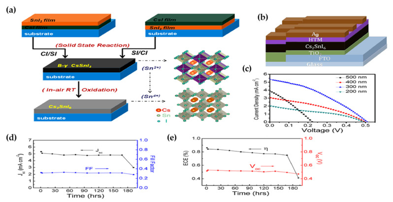
Abstract
Despite the progressive enhancement in the flexibility of Pb-based perovskites for optoelectronic applications, regrettably, they are facing two main challenges; (1) instability, which originates from using organic components in the perovskite structure, and (2) toxicity due to Pb. Therefore, new, stable non-toxic perovskite materials are demanded to overcome these drawbacks. The research community has been working on a wide variety of Pb-free perovskites with different molecular formulas and dimensionality. A variety of Pb-free halide double perovskites have been widely explored by different research groups in search for stable, non-toxic double perovskite material. Especially, Cs-based Pb-free halide double perovskite has been in focus recently. Herein, we present a review of theoretical and experimental research on Cs-based Pb-free double halide perovskites of structural formulas Cs2M+M3+X6 (M+ = Ag+, Na+, In+ etc.; M3+= Bi3+, In3+, Sb3+; X = Cl−, Br−, I¯) and Cs2M4+X6 (M4+ = Ti4+, Sn4+, Au4+ etc.). We also present the challenges faced by these perovskite compounds and their current applications especially in photovoltaics alongside the effect of metal dopants on their performance.
Keywords: Cs-based Pb-free double halide perovskites, applications of double halide perovskites, doping
1. Introduction
During the last ten years, Pb-based perovskites as a promising subcategory of solar cell materials have attracted intense attention of the research community due to their unique advantages. In 2009, for the first time, Miyasaka et al. published a paper demonstrating the use of methylammonium lead triiodide (CH3NH3PbI3) as a light absorber instead of dye in dye sensitized solar cells (DSSCs) with an efficiency of 3.8% [1]. A few years after, a solid hole transporting layer named Spiro-MeOTAD replaced the liquid electrolyte in these structures which helped to increase the efficiency of perovskite solar cells (PSCs) to 9.7% [2]. Since then, the number of research articles in this field exponentially increased, and considerable advances in power conversion efficiency exceeding 25.2% are reported for PSCs [3].
The general formula of perovskite is ABX3 where A is a monovalent cation (methylammonium (MA+), formamidinium (FA+), or Cs+), B is a divalent metal (Pb2+) and X is halide anion (I−, Br−, and Cl−) [4]. Depending on A-cation, perovskites can be categorized into (1) organic-inorganic hybrid or (2) all-inorganic halide perovskite [5]. Possession of unique advantages including high extinction coefficient [6,7], low exciton binding energy [8], and tunable bandgap [9], turn the metal halide perovskites as superb carrier transporters and photo absorbers. It is noteworthy that these materials are also used not only in PSCs, but also in other optoelectronic devices, such as light-emitting diodes (LEDs) [10], lasers [11], photodetectors [12,13], and X-ray detectors [14].
However, there are few drawbacks regarding Pb-based halide perovskites as an active layer in PV applications, which must be tackled in order to achieve full scale application [15]. The first concern is of lead in perovskite materials as Pb is a well-known heavy metal [16]. Exposure to lead causes a detrimental effect on humans and surprisingly the absorptions of this metal in children’s body is four to five times larger than an adult’s human body [17]. Acute exposure to Pb can result in kidney damages, brain damages, and gastrointestinal disease, and chronic exposure to lead may induce adverse effects on the blood pressure, kidneys, central nervous system, and vitamin D metabolism [18,19]. Pb also can replace Calcium and interact with proteins and, as a result, disrupts the neurotransmitter release and bone mineral density [17,19]. In order to decrease the usage amount of hazardous materials, including Pb in electronic and electric devices, different restrictions of hazardous substances (RoHS) policies were implemented in many countries with the aim of reducing the risk to both human health and environment [17,20].
The second challenge with organic-inorganic PSCs is the weak operational stability of organic lead halide perovskite due to organic formamidinium (FA+) or methylammonium (MA+) which make them vulnerable to degradation upon exposure to light, high temperature and humidity [21,22].
Accordingly, in order to achieve more stable and non/less toxic PSCs, different strategies have been adopted including (1) utilization of a protective layer around perovskite material as well as resilience development of perovskite layer [23], (2) using mixed halide anions and mixed A- cations [24,25], (3) applying of additives and doping agents [25,26,27] such as monovalent (Cu+ [28], Ag+ [28,29], Na+ [28,30], etc.), divalent (Mn2+ [30], Sr2+[31], Zn2+ [32], etc.) and trivalent metal ions (Bi3+ [33] and Sb3+ [34]), and (4) synthesis of 2D halide perovskites [35,36,37]. However, these approaches were not able to overcome the aforementioned challenges adequately. Therefore, new designs of perovskite materials, applicable to all optoelectronic devices, have been suggested through theoretical and experimental studies by different research groups where Pb2+ and MA+/FA+ were replaced by less/non-toxic inorganic components.
In a number of studies, it has been shown that incorporation of Cs+ instead of applying MA+/FA+ in perovskite structure has led to a broad band of advantages, including decreasing crystallization temperature, enhancing the absorption before and after annealing, decreasing the side phases, improving photogenerated carrier lifetime, and reducing the density of trap states, etc., which has resulted in higher PCEs for the PSCs and has also led to better stability of perovskite structure [38]. In order to tackle the toxicity issue, Sn2+ and Ge2+ ions have been suggested as the first logical substitution of Pb2+ in perovskite structure since these metal ions have similar electronic configuration of s2p2 and thereby similar chemical properties [39,40,41]. It is shown that Sn-based perovskites provide numerous advantages such as narrower bandgap [42], higher charge carrier mobilities [42], and longer diffusion length [43] compared to their Pb analogs. But the idea of using these ions did not meet the expected results because Sn2+ and Ge2+ ions tend to be oxidized to their stable oxidations state of 4+ [44]. Bi3+ and Sb3+ with similar isoelectronic structure were the other explored alternatives to Pb2+ ion [41,45]. However, their chemical bonding preference and their 3+ oxidation state make them suitable for fitting in tetragonal structure in A3M2I9 perovskite, meaning that they have a low-dimensional structure (2D) causing poor performance [5,45,46,47].
Double perovskite crystals with a general formula A2M+M3+X6 and A2M4+X6 (where M is the metal ion) are the other alternative and promising lead-free perovskite materials, that have been proposed for photovoltaic and other optoelectronic applications [48,49,50]. In this structure, two different metal ions with different oxidation states of 1+ and 3+, are substituted by two divalent Pb2+ metal ion in a three-dimensional perovskite structure. The space group of this lead-free perovskite materials is Fm3 with two different octahedra groups comprised of M+ and M3+ in a rock salt face-centered cubic structure [50].
This review aims to focus on experimental and theoretical studies of Cs-based inorganic Pb-free double halide perovskite materials in the form of Cs2M+M3+X6 (M+ = Ag+, Na+, In+ etc.; M3+ = Bi3+, In3+, Sb3+; X = Cl−, Br−) and Cs2M4+X6 (M4+ = Ti4+, Sn4+, Au4+ etc.) alongside their results and applications in different optoelectronic devices, including solar cells, light-emitting diodes (LEDs), X-ray detectors, and photodetectors. We also present the effect of elemental substitution on the performances of these materials.
2. Double Halide Perovskites
The two key features of Pb-based halide perovskites (ABX3) which result in excellent optoelectronic properties are high symmetry of BX6 octahedral and the unique electronic configuration of Pb2+ (6s2 6p0) which leads to strong Pb 6s- I 5p antibonding coupling [51]. Therefore, to obtain a promising Pb-free solar absorber candidate in perovskite structure, the symmetry of octahedra should be preserved. Octahedral rotation distortion, like twisting or tilting, may affect the symmetry properties of target crystals. In order to maintain high stability and high symmetry of cubic structure, two different parameters named Goldschmidt’s tolerance factor (t = RA+RX)/(√2(RB+RX)), and octahedral factor (μ = RB/Rx) should be considered. For ideal perovskite structure “t” is between 0.8 and 1 and “μ” is larger than 0.414 [52].
Meanwhile, some research groups have considered other factors for designing efficient Pb-free double halide perovskites for solar cell applications. Meng et al. [53], by carrying out a computational study suggested that inversion symmetry-induced parity-forbidden transitions should be considered for designing new double halide perovskites. In their study, they indicated that for most double halide perovskites with a direct bandgap like Cs2AgInCl6, transition from valance band maximum (VBM) to conduction band minimum (CBM) is forbidden because of inversion symmetry in their structure. And this is likely one of the reasons for their poor photovoltaic performance [53]. Xiao et al. [51] demonstrated that for gaining optimal and efficient lead-free halide perovskites for photovoltaic performance, besides structural dimensionality, electronic dimensionality should also be taken into account. This new concept explains that connectivity of electronic orbitals, which form the conduction band minimum (CBM) and valance band maximum (VBM), is another essential parameter for understanding the photovoltaic properties of all reported perovskites. Perovskites with three-dimensional (3D) crystal and electronic structures are the most desired for good photovoltaic performance [51].
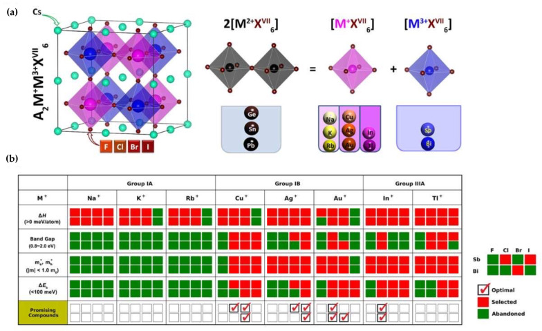
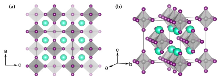
Considering all important and affecting parameters, Zhao et al. [54], through the first-principals calculation exploited the cation transmutation idea to explore all-inorganic Pb-free double halide perovskites for photovoltaic application by replacing Pb2+ by Bi3+ or In3+. Among 64 different potential considered candidates, only 11 compounds with intrinsic thermodynamic stability, suitable band gaps, small carrier effective masses, and low exciton binding energies have been identified as promising absorbers. Figure 1a,b show the screening process of the materials based on properties like decomposition enthalpy (∆H), carrier effective masses (me* and mh*) and exciton binding energy (∆Eb) [54]. In the following, we will present the successfully investigated Cs-based Pb-free all-inorganic double halide perovskites with their current potential applications in various optoelectronic devices, along with the effect of elemental substitution on their optical and structural characterizes.
Figure 1.
(a) Suggested structure of double halide perovskite with a formula of A2B+B3+X6 using the idea of transmutation and; (b) materials screening process considering the decomposition enthalpy (∆H), bandgap (Eg), carrier effective masses (me* and mh*) and exciton binding energy (∆E). Reproduced with permission from [54]. Copyright 2017, American Chemical Society.
2.1. Cs/Bi3+-Based Double Halide Perovskites
For many decades, Bi (bismuth) has been applied as an eco-friendly and non-toxic metal with interesting properties in diverse applications. Bi has been introduced as a suitable replacement for Pb because of comparable density and similar electronic configuration [55,56]. Due to the significant features, Bi has been one of the first examined candidates for developing Pb-free double halide perovskite materials for PV applications [48,49,50]. This idea was developed by three independent research groups which simultaneously, published their successful investigations by replacing Pb2+ with heterovalent substitution of Bi3+ and Ag+ to form a lead-free double halide perovskite in 2016 [48,49,50].
For the sake of completeness, we have provided a list of Cs/Bi3+-based halide double perovskites along with their theoretical and experimental bandgap values and other information including morphology and applied synthetic methods in Table 1. In order to get a good overview, we present the results from theoretical and experimental studies separately.
Table 1.
Summary of prepared double halide perovskite samples based on inorganic Cs/Bi3+.
| Compounds | Morphology | Synthetic Method |
Optical Transition | Theoretical Bandgap | Experimental Bandgap | Characterization Techniques | Theoretical Calculation | Reference |
|---|---|---|---|---|---|---|---|---|
| Cs2AgBiBr6 | Powder and single crystals |
Solution-based process using hydrohalic acid | Indirect | - | 1.95 eV | PL, UV-Vis spectroscopy, TGA, PXRD | - | [48] |
| Cs2AgBiBr6 | polycrystalline | Solution-based process using hydrohalic acid process and solid-state reaction | Indirect | 2.06 eV | 2.19 eV | PL, UV-vis spectroscopy, XRPD | DFT-VASP | [49] |
| Cs2AgBiBr6 | Single crystals | Solution-based process using hydrohalic acid with high pressure treatment | Indirect | 2.36 eV | ~1.7 eV | UV-Vis spectroscopy, ADXRD, Raman | DFT-LDA in CASTEP | [56] |
| Cs2AgBiBr6 | Single crystals | Solution-based process using hydrohalic acid process and solid-state reaction | Indirect | 1.8 eV | 1.9 eV | PXRD, UV-Vis spectroscopy, PL | DFT-LDA+SOC, GW | [57] |
| Cs2AgBiBr6 | - | - | Pseudo- direct | 0.44 eV | - | - | DFT/VASP/PAW pseudopotentials/PBEsol, HSE06+SOC | [58] |
| Cs2AgBiBr6 | Nanocrystals | Hot-injection method | Indirect | - | 2.33 eV | TEM, HTEM, XRD, UV-Vis, PL | - | [59] |
| Cs2AgBiBr6 | Single crystals and thin film | Solution-based process using hydrohalic acid, slow precipitation method | Indirect | - | 2.0 eV | TRPL, PL, PDS, UV-Vis spectroscopy, X-ray photoemission | - | [60] |
| Cs2AgBiBr6 | Single crystals |
Solution-based process using hydrohalic acid |
Indirect | 2.1 eV | 2.12 eV | Raman, PLE | DFT/Crystal17 | [61] |
| Cs2AgBiBr6 | Thin film | Solution-based process | Indirect | 1.84 eV | 2.10 eV | UV-Vis spectroscopy | DFT/PAW/VASP, HSE06+SOC, QTAIM/CRITIC2 | [62] |
| Cs2AgBiBr6 | Polycrystals | Mechanochemical | Indirect | - | 2.0 eV | XRD, XPS, UV-Vis spectroscopy, TG-DSC, TCSPC, XRF | - | [63] |
| Cs2AgBiBr6 | Thin film | Solution-based process using DMSO | Indirect | - | 2.12 eV | XRD, UV-Vis spectroscopy, PL, SEM | - | [64] |
| Cs2AgBiBr6 | Thin film | Solution-based process using DMSO | Indirect | - | 2.02 eV | XRD, UV-Vis spectroscopy, PL, SEM, EDX, XPS, AFM | - | [65] |
| Cs2AgBiBr6 | Thin film | Solution-based process using DMSO | Indirect | - | 2.09 eV | XRD, UV-Vis spectroscopy, PL, SEM | - | [66] |
| Cs2InBiBr6 | Powder and single crystals | solid-state reaction |
Direct | 0.33 eV | - | PXRD, SCXRD | DFT-VASP, PBE+SOC | [67] |
| Cs2AgBiCl6 | Polycrystalline | Solution-based process using hydrohalic acid process and solid-state reaction | Indirect | 2.62 eV | 2.77 eV | PL, UV-vis spectroscopy, XRPD | DFT-VASP | [49] |
| Cs2AgBiCl6 | Powder | Solid-state reaction | Indirect | 3.0 eV | 2.2 eV | PXRD, UV-Vis spectroscopy, PL | DFT-LDA Hybrid PBE0 |
[50] |
| Cs2AgBiCl6 | Single crystals | Solution-based process using hydrohalic acid process and solid-state reaction | Indirect | 2.4 eV | 2.2 eV | PXRD, UV-Vis spectroscopy, PL | DFT-LDA+SOC, GW |
[57] |
| Cs2AgBiCl6 | Nanocrystals | Hot-injection method | Indirect | - | 2.89 eV | TEM, HTEM, XRD, UV-Vis spectroscopy, PL | - | [59] |
| Cs2AgBiCl6 | Single crystals and thin film | Solution-based process using hydrohalic acid, slow precipitation method | Indirect | - | 2.5 eV | TRPL, PL, PDS, UV-Vis spectroscopy, X-ray photoemission | - | [60] |
| Cs2InBiCl6 | Powder and single crystals | solid-state reaction | Direct | 0.88 eV | - | PXRD, SCXRD | DFT-VASP, PBE+SOC | [67] |
| Cs2InBiCl6 | - | - | Direct | 1.02 eV | - | - | DFT, HSE+SOC, PBE+SOC | [54] |
| Cs4CdBi2Cl12 | Single crystals | Solvothermal | Direct forbidden | 3.58 eV | 3.23 eV | PXRD, SC-XRD, TGA, EDS, PL, PLE, TRPL, UV-Vis-NIR spectroscopy | DFT/VASP/PAW, GGA-PBE, HSE+SOC | [68] |
2.1.1. Cs2M+Bi3+X6: Theoretical Studies
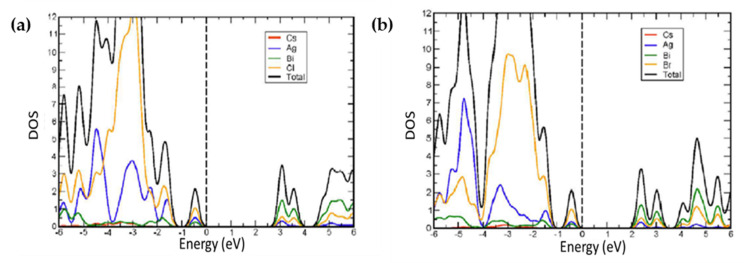
McClure et al. [49] studied Cs2AgBiBr6 and Cs2AgBiCl6 as the two first potential double halide perovskite compounds, by employing DFT analysis on VASP simulation software. The indirect bandgap of 2.06 eV for Cs2AgBiBr6 and 2.62 eV for Cs2AgBiCl6 were obtained as presented in Table 1. According to the atomic partial density of states, the indirect bandgap resulted from the combination of Ag 4d orbitals with halogens 3p/4p orbitals which led to sufficient changes in the valence band as shown in Figure 2a,b. The study has also shown that hole effective masses were lighter (Cs2AgBiCl6 = 0.15 mh; Cs2AgBiBr6 = 0.14 mh) than their CsPbX3 analogs (CsPbCl3 = 0.35 mh; CsPbBr3 = 0.37 mh) and the electron effective masses were also comparable (Cs2AgBiCl6 = 0.53 me; Cs2AgBiBr6 = 0.37 me) with CsPbX3 compounds (CsPbCl3 = 0.41 me; CsPbBr3 = 0.34 me).
Figure 2.
Atomic partial density of states for; (a) Cs2AgBrBr6 and; (b) Cs2AgBrCl6. Reproduced with permission from [49]. Copyright 2016, American Chemical Society.
Volonakis et al. [50] selected a different range of metals comprised of pnictogen (Bi3+, Sb3+ (group VA of periodic table)) and noble metals (Ag+, Au+, Cu+) for computational and experimental studies. By using density functional theory in the local density approximation (DFT-LDA), they found all these compounds to have indirect bandgaps of less than 2.7 eV. By changing both halides from I− to Cl− and the pnictogen from Bi3+ to Sb3+, the bandgap was seen to be increasing. However, changing of the noble metals did not have any effect on this trend, since CBM and VBM mostly have pnictogen-p and halogen-p character, respectively. This means that by moving up in halogen (from I− to Cl−) and pnictogen group (from Bi3+ to Sb3+) in the periodic table, their p-state energy will be decreased, and consequently both VBM and CBM will be lowered. Another notable examined parameter was the smaller carrier effective masses in these compounds (between 0.1 and 0.4) compared to relevant MAPbI3.
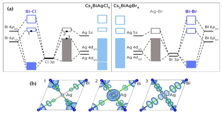
Filip et al. [57] focused on the electronic properties of Cs2AgBiX6 (X = Cl¯and Br−) compounds through theoretical calculations. To obtain accurate bandgap values, they used the experimental crystal structures data within the DFT-LDA calculation in the quantum espresso suit with and without spin-orbit coupling. Based on obtained molecular orbitals diagram through the atom-projected density of states, they indicated that because of smaller energy difference in Ag-d and Br-p states in comparison with Ag-d and Cl-p, valence band width was reduced. Moreover, the delocalized nature of Br-4p orbitals resulted in more overlaps with Bi-6p, and thereby the width of conduction band increased as illustrated in Figure 3. Study of quasiparticle calculation for determination of the bandgap (1.8 eV for Cs2AgBiBr6 and 2.4 eV for Cs2AgBiCl6) showed a good agreement with their experimental findings (1.9 eV for Cs2AgBiBr6 and 2.2 eV for Cs2AgBiCl6) [57].
Figure 3.
(a) Comparison between the molecular orbitals diagram of Cs2AgBrCl6 and Cs2AgBrBr6 and; (b) Square modulus of the wave functions for states marked from 1 to 3 on the molecular orbital diagram of Cs2BiAgCl6. 1 represents the Bi-6p1/2/halide-p antibonding orbitals at the bottom of the conduction band (at Γpoint). 2 is the antibonding Ag-5s/halide-p at the L-point of the conduction band), while 3 corresponds to the Ag-4d/halide-p antibonding orbitals found at the top of the valence band (at X-point). Reproduced with permission from [57]. Copyright 2016, American Chemical Society.
Xiao et al. [69] investigated the thermodynamic stability of Cs2AgBiBr6 by DFT calculation, and claimed that Ag vacancies were shallow accepters that resulted in intrinsic p-type conductivity in Cs2AgBiBr6. On the other hand, the existence of some dominant deep defects such as Bi vacancies (VBi) and AgBi antisites give rise to poor photovoltaic performance. Accordingly, Xiao et al. [69], in order to reduce the formation of deep defects, suggested that the synthesis of material preferably should be done under Bi-poor/Bi-rich growth conditions.
Xiao et al. [67] studied Cs2In+M3+X6 (M = Bi3+, and X = halogens) double halide perovskites, both theoretically and experimentally. Their results indicated that high-energy-laying in 5s2 state of In+ is substantially responsible for promising photovoltaic performance. However, due to the oxidation of In+ to In3+, and the reduction of Bi3+ to its metal form, the whole perovskite structure becomes unstable.
Since optimizing the bandgap is an important factor for enhancing the efficiency of PSCs, Yang et al. [58] proposed by changing the atomic arrangement in Cs2AgBiBr6 crystal structure, the bandgap can be narrowed. Using Monte Carlo and DFT calculations performed in VASP code by employing HSE06 with SOC, they showed that increasing the temperature up to 1200 K would increase the energy and consequently, phase transitions would occur. In this condition, Ag+ and Bi3+ ions randomly occupy the M-site in A2M+M3+X6 structure, and this leads to reduction of bandgap from 1.93 eV to pseudo-direct bandgap of 0.44 eV.
2.1.2. Cs2M+Bi3+X6: Experimental Studies
In this section, we provide detailed synthesis methods of Cs/Bi3+-based double halide perovskites and their characterization results. This section based on obtained morphologies is divided into two categories, namely, crystalline and thin-film structures in 1.2.1 and 1.2.2, respectively. This detailed information of the experimental studies is also summarized in Table 1.
Cs2M+Bi3+X6: Single-Crystals, Polycrystalline and Nanocrystals-Based Perovskites
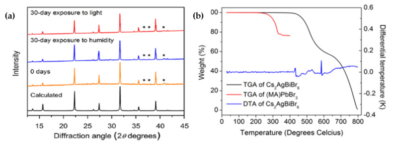
Slaveney et al. [48] synthesized double halide perovskite Cs2AgBiBr6 with photoluminescence (PL) lifetime of approximately 660 ns with an indirect bandgap of 1.95 eV. Compared to MAPbI3, this compound showed higher stability against moisture and heat and had long room-temperature PL lifetime (736 ns to 1 μs for MAPbI3 films) which is a good characteristic for photovoltaic performance. Interestingly, the obtained PXRD (Powder X-ray diffraction) pattern did not show any evidence of material decompaction as shown in Figure 4a. Thermogravimetric analysis (TGA) showed that the material was stable up to 430° which could be due to the replacement of unstable organic cation MA+ with Cs+ ions as depicted in Figure 4b.
Figure 4.
(a) PXRD pattern of Cs2AgBiBr6 after exposure to humidity (55% RH) and light (0.75 Sun), * and ** refers to the signals from sample holder; (b) Thermogravimetric analyses of Cs2AgBiBr6 and (MA)PbBr3 at a scan rate of 5 °C/min and 1 °C/min, respectively. Solid (MA)PbBr3 shows an initial mass loss at 176 °C. Solid Cs2AgBiBr6 shows an initial mass loss at 430 °C. DTA of Cs2AgBiBr6 shows no phase changes until the mass loss onset. Reproduced with permission from [48]. Copyright 2016, American Chemical Society.
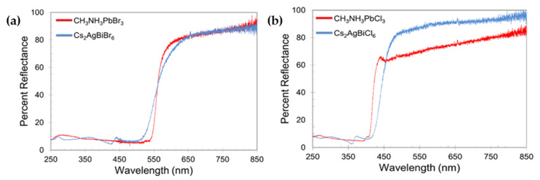
McClure et al. [49] prepared polycrystalline Cs2AgBiBr6 and Cs2AgBiCl6 by applying solid state and solution-based methods. The PXRD analysis confirmed the 3D structure of these compounds in corner connected octahedra with alternating Ag+ and Bi3+ in a rock salt ordering. However, according to PXRD and Rietveld refinements, due to large number of displacement parameters (Beq) and low bond valence sum of Cesium ion, phase transition could be expected below room temperature. UV-Vis diffuse reflectance spectra showed significant similarities between Cs2AgBiX6 and Pb-based analogs (CH3NH3PbX3) although there were some minor differences at photon energies above the absorption onset as shown in Figure 5a,b. Using Kubelka-Munk equation and Tauc plot, the optical indirect bandgap of 2.19 eV and 2.77 eV were obtained for Cs2AgBiBr6 and Cs2AgBiCl6, respectively which were close to their theoretically calculated values (2.06 eV for Cs2AgBiBr6 and 2.62 eV for Cs2AgBiCl6) [46]. In order to investigate the light and chemical stability, samples were placed in both dark and light conditions under ambient environment for one month. The obtained UV-Vis diffuse reflectance spectra analysis of the samples after 14 and 28 days exhibited that Cs2AgBiBr6 was less light stable than Cs2AgBiCl6 and the conclusion was that encapsulation of the structures might be needed for PV application.
Figure 5.
Diffuse reflectance spectra of; (a) MAPbBr3 and Cs2AgBrBr6; (b) MAPbCl3 and Cs2AgBrCl6. Reproduced with permission from [49]. Copyright 2016, American Chemical Society.
Volonakis et al. [50] successfully prepared single-phase Cs2AgBiCl6 samples through the solid-state reaction in a sealed fused silica ampoule. The structural and optical measurements by using single-crystal X-ray diffraction (SCXRD), UV-Vis spectroscopy and photoluminescence showed that the Cs2AgBiCl6 perovskite belongs to Fm3 space group while BiCl6 and AgCl6 octahedra are alternately placed in a rock-salt face-centered cubic structure with an indirect bandgap of 2.2 eV.
It is noticeable that the three abovementioned articles [48,49,50] presented different experimental bandgap values for Cs2AgBiCl6 (2.2 eV to 2.7 eV) and Cs2AgBiBr6 (1.83 eV to 2.19 eV) which is mainly due to the different synthesis methods (solid state preparation and solution processing) as well as utilizing different measurement techniques and methods such as UV-Vis spectroscopy and UV-Vis diffuse reflectance, Tauc plot, etc. for calculating bandgaps [57]. To overcome these discrepancies, Filip et al. [57] by employing the same solid state and solution-based synthesis methods prepared stable Cs2AgBiBr6 and Cs2AgBiCl6 single crystals under ambient environment. Through the optical measurements including UV-Vis spectroscopy and PL, they obtained an indirect bandgap of 1.9 eV and 2.2 eV for Cs2AgBiBr6 and Cs2AgBiCl6, respectively.
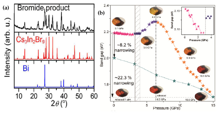
Xiao et al. [67] used In+ instead of Ag+ and synthesized Cs2In+Bi3+X6 (X = halogens) double halide perovskites using solid-state reaction method. Their experimental investigation using SCXRD (Single Crystal X-ray diffraction) and PXRD exhibited that In+-based halide double perovskites spontaneously decomposes into In3+-based ternary materials such as CsInI4, Cs3In2Br9 and Cs3In2Cl9 (Figure 6a). In fact, In1+ is an unstable and unusual oxidation state in inorganic solids and there are only a few reported double perovskite compounds based on In+ [70,71].
Figure 6.
(a) PXRD pattern of the bromide product and simulated PXRD pattern for Cs3In2Br9 and Bi. Reproduced with permission [67]. Copyright 2017, American Chemical Society; (b) evolution of bandgap in Cs2AgBrBr6 structure at high pressure with representative optical micrographs indicating piezochromic transitions. Reproduced with permission from [56]. Copyright 2017, Wiley-VCH.
Li et al. [56] by applying the high-pressure method, which previously had been used for size-dependent phase transformation [72] indicated that the bandgap of Cs2AgBiBr6 through high-pressure method was reduced by 22.3% from 2.2 eV to 1.7 eV. Using UV-vis spectroscopy as optical measurement, they observed by increasing the pressure to ~15 GPa, the color of the product changed to brown black and absorption peak exhibited a continues redshift. Interestingly, even after releasing the pressure, the bandgap value was observed to be around ≈2.0 eV (Figure 6b).
The angle dispersive X-ray diffraction (ADXRD) analysis of the sample illustrated that by employing a wide range of pressure, a minimized octahedral tilting through ab plane occurs, and this decreased the Bi-Br-Ag bond angle from 180° to 166.4°. It is believed that this is one of the major factors of narrowing the bandgap of Cs2AgBiBr6.
In 2018, Hoye et al. [60] explored the carrier lifetime and recombination mechanism in the Cs2AgBiBr6 thin film in more detail. Both single crystals and thin film of Cs2AgBiBr6 were prepared through the slow precipitation method of saturated solution at low temperature. Based on optical measurements, the fundamental carrier lifetime for Cs2AgBiBr6 thin film was shown to be 1.4 μs. The carrier density of Cs2AgBiBr6 was calculated to be 2.2 × 1016 cm−3 under 1 sun, which was larger than MAPbI3 steady-state carrier density (5.2 × 1015 cm−3 under 1 sun). This clearly indicates the benefit of utilizing Cs2AgBiBr6 in solar cells.
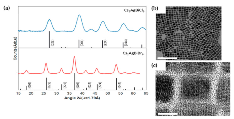
Bekenstein et al. [59] selected hot-injection method for preparation of Cs2AgBiBr6 nanocrystals which previously was employed for synthesis of CsPbX3 and CsPbCl3 NCs by Protesescu et al. [73], and Xu et al. [74], respectively. The XRD and HRTEM analysis indicated that the crystals had the cubic Fm3 structure with the side length of 8–15 nm as shown in Figure 7a–c.
Figure 7.
(a) XRD pattern of Cs2AgBiBr6 (red) and Cs2AgBiCl6 (blue) NCs in comparison with reported XRD patterns where scale bars refer to the other published XRD patterns for Cs2AgBiBr6 and Cs2AgBiBr6 perovskites; (b) low-resolution and; (c) high-resolution TEM images of Cs2AgBiBr6 NCs showing atomic lattice fringes. Reproduced with permission from [59]. Copyright 2018, American Chemical society.
The color of the sample was distinctly yellow, which was different from the previously prepared samples’ color based on solid-state and solution-processed methods (orange-red) [48,49,50]. The stability of the NCs was examined through the changing of solvents and changing of ligands. Solvents with higher polarity caused less stable NCs and by introducing the excess amount of primary and tertiary amines, absorption and emission features of the sample disappeared, which suggested that Cs2AgBiBr6 and CsPbI3 had similar surface chemistry. Furthermore, it was demonstrated [59], due to the Ag diffusion, reduction and coalescence, Cs2AgBiBr6 NCs in solution were structurally unstable and degraded to Cs3Bi2Br9 and Cs3BiBr6 byproduct NCs. However, by controlling the solvents evaporation rate, less degradation was occurred on NCs superlattices assembled into the ordered NC solids including strong ligand-ligand interaction.
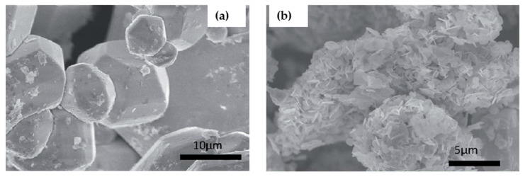
Zhang et al. [75], as presented in Table 2, replaced Ag+ in Bi-based halide double perovskite with Na+ ion for fabricating the solar cell, and Cs2NaBiI6 perovskite was synthesized by facile one-step hydrothermal process. The material showed tolerance factor of 0.849 and octahedral factor of 0.466 with bandgap of 1.66 eV. The SEM images showed by increasing the concentration of solvent (HI), up to 6 M, the crystal growth got improved as shown in Figure 8a,b.
Table 2.
Prepared device architecture and photovoltaic parameters of Cs-based double halide perovskite solar cells.
| Perovskite Material |
Year | Device Architecture |
Perovskite Deposition Method | Voc [V] |
Jsc [mA cm−2] |
FF | PCE [%] |
Reference |
|---|---|---|---|---|---|---|---|---|
| Cs2AgBiBr6 | 2017 | FTO/c-TiO2/mp-TiO2/perovskite/spiro-OMeTAD/Au | One-step spin coating with preheating | 0.98 | 3.93 | 0.63 | 2.43 | [77] |
| Cs2AgBiBr6 | 2018 | ITO/SnO2/perovskite/P3HT/Au | One-step spin coating with low-pressure assisted method | 1.04 | 1.78 | 0.78 | 1.44 | [78] |
| Cs2AgBiBr6 | 2018 | ITO/ c-TiO2/perovskite/spiro-OMeTAD/Au | One-step spin coating | 1.06 | 1.55 | 0.74 | 1.22 | [79] |
| Cs2AgBiBr6 | 2018 | FTO/c-TiO2/mp-TiO2/perovskite/PTAA/Au | One-step spin coating with anti-solvent dropping methodology | 1.02 | 1.84 | 0.67 | 1.26 | [80] |
| Cs2AgBiBr6 | 2018 | ITO/Cu-NiO/perovskite/C60/BCP/Ag | One-step spin coating with anti-solvent dropping methodology and post-annealing | 1.01 | 3.19 | 0.69 | 2.23 | [81] |
| Cs2NaBiI6 | 2018 | FTO/c-TiO2/perovskite/P3HT/Au | One-step spin coating | 0.47 | 1.99 | 0.44 | 0.42 | [75] |
| Cs2AgBiBr6 | 2018 | FTO/c-TiO2/mp-TiO2/perovskite/ spiro-OMeTAD/Au | Sequential vapor deposition with two step annealing | 1.12 | 1.79 | - | 1.37 | [82] |
| Cs2AgBiBr6 | 2019 | FTO/TiO2/perovskite/SpiroOMeTAD/MoO3/Ag | Vacuum sublimation and one-step spin coating | 1.01 | 3.82 | 0.65 | 2.51 | [83] |
| Cs2AgBiBr6 | 2020 | ITO/SnO2/perovskite/Zn-Chl /Ag | One-step spin coating | 0.99 | 3.83 | 0.736 | 2.79 | [64] |
| Cs2AgBiBr6 | 2020 | FTO/c-TiO2/mp-TiO2/perovskite/ N719/spiro-OMeTAD/Au | One-step spin coating with two-step heating process. | 1.06 | 5.13 | 0.524 | 2.84 | [65] |
| Cs2AgBiBr6 | 2021 | FTO/c-TiO2/mp-TiO2/C-Chl/perovskite/spiro-OMeTAD/Au | One-step spin coating | 1.04 | 4.09 | 0.73 | 3.11 | [66] |
| (Cs1-xRbx)2AgBiBr6 | 2019 | ITO/SnO2/perovskite/spiro-OMeTAD/Au | One-step spin coating with low-pressure assisted method | 0.99 | 1.93 | 0.78 | 1.52 | [84] |
| Cs2AgSbBr6 | 2019 | FTO/c-TiO2/mp-TiO2/perovskite/spiro-OMeTAD/Au | One-step spin coating | 0.35 | 0.080 | 0.35 | 0.01 | [85] |
| Cs2SnI6 | 2017 | FTO/c-TiO2/perovskite/P3HT/Ag | Two-step sequential vapor deposition | 0.51 | 5.41 | 0.35 | 0.96 | [86] |
| Cs2TiBr6 | 2018 | FTO/TiO2/C60/perovskite/P3HT/Au | Facile low-temperature vapor deposition | 1.02 | 5.69 | 0.564 | 3.3 | [87] |
Figure 8.
(a) multiple shuttle-like crystals from high acidity synthesis and; (b) clusters of nano-plates from non-acid synthesis. Reproduced with permission from [75]. Copyright 2018, Royal Society of Chemistry.
In 2019, Zelewski et al. [61] by combination of photoluminescence excitation (PLE) and Raman spectroscopy demonstrated that the PL emission in Cs2AgBiBr6, was dominated by the strong electron-phonon coupling due to the relatively large Huang-Rhys factor (S = 11.7). It was also revealed that the excitation resonant of the color center in ionic crystals of Cs2AgBiBr6 was more responsible for the PL emission rather than band to band transition. It was also proven that the color centers of ionic crystals were coupled with crystal lattice vibrations [76]. Local lattice deformation would occur if any of these centers were occupied. This led to energy offset in color center between ground state (unoccupied) and excited states (occupied) [61].
Cs2M+Bi3+X6: Film-Based Perovskites
In following section, we present the studies in which Cs2M+Bi3+X6 perovskites prepared as thin film for PV application and the results are presented in Table 2.
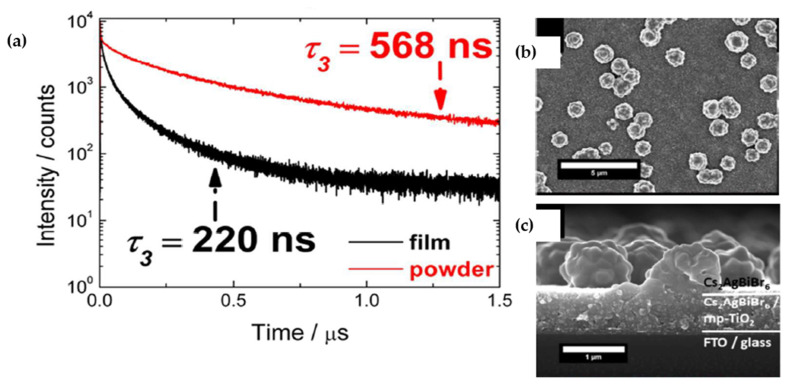
Although other research groups were employing halide acids as solvent, in 2017, Greul et al. [77] for the first time used dimethyl sulfoxide (DMSO) as the solvent in the synthesis of Cs2AgBiBr6 film. By annealing at temperatures higher than 250° all the side phases such as AgBr and Cs3Bi2Br9 were removed. They reported that adopting a preheating step at 75° right before the spin coating of Cs2AgBiBr6 film led to enhanced surface coverage and increased optical absorption. However, the Cs2AgBiBr6 film exhibited faster photoluminescence decay time (220 ns) in comparison with polycrystalline powders (568 ns) due to their large concentration of trap states (Figure 9a). Also, SEM images of the film indicated some agglomeration on the surface of spin coated film which contributed to the fast crystallization process (Figure 9b,c).
Figure 9.
(a) TCSPC decays of a Cs2AgBiBr6 film on glass and polycrystalline powder; (b) SEM top-view and; (c) SEM cross-section images of the Cs2AgBiBr6 film prepared with a 75 °C preheating step on mp-TiO2. Reproduced with permission from [77]. Copyright 2017, Royal Society of Chemistry.
Wu et al. [78] employed low-pressure assisted (LPA) method for preparation of Cs2AgBiBr6 film. In this method, as-synthesized Cs2AgBiBr6 powder [48] was dissolved in DMSO and then spin-coated on an ITO/glass substrate. The prepared film then was quickly moved to a low-pressure chamber (20 Pa) and finally was annealed thermally (Figure 10a,b). Using the LPA method led to enhanced crystallinity and grain size.
Figure 10.
(a) images of Cs2AgBiBr6 powder and Cs2AgBiBr6 solution in DMSO and; (b) the film fabrication process diagram. Reproduced with permission from [78]. Copyright 2018, Wiley-VCH.
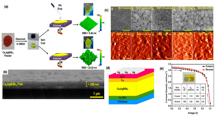
Gao et al. [81] inspired by the LPA synthesis method [88], adopted an anti-solvent dropping methodology for synthesis of Cs2AgBiBr6 film as depicted in Figure 11a,b. Combination of this method with post-annealing at high temperature resulted in smooth morphology, micro-sized grains and high crystallinity (Figure 11c).
Figure 11.
(a) Schematic illustration of the spin-coating process (with and without anti-solvent dropping protocol); (b) Cross-sectional SEM image of a Cs2AgBiBr6 film obtained by IPA dipping; (c) SEM images and AFM images of Cs2AgBiBr6 films annealed at different temperatures; (d) Structure of the inverted PSC devices fabricated in this work and; (e) J-V curves of the best-performing device based on Cs2AgBiBr6 films obtained at different fabrication conditions. Reproduced with permission from [81]. Copyright 2018, Wiley-VCH.
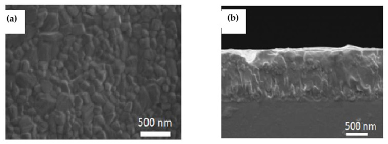
Pantaler et al. [80] used chlorobenzene as anti-solvent before the annealing step during the film formation to obtain the smooth layer without any pinholes (Figure 12a). The SEM images of the film showed crystal grain size of 80 nm and 200 nm thickness (Figure 12b).
Figure 12.
(a) Top-view SEM image of obtained Cs2AgBiBr6 film by spin coating at room temperature using the anti-solvent treatment with chlorobenzene; (b) cross-section SEM image of FTO/c-TiO2/m-TiO2/double perovskite sample, upon annealing at 280 °C. Reproduced with permission from [80]. Copyright 2018, American Chemical Society.
Wang et al. [82] employed the sequential-vapor-deposition procedure for the synthesis of Cs2AgBiBr6 film as depicted in Figure 13. To obtain an optimized film, annealing was carried out in two different steps. The film was first annealed at 200° for 5 h, which was then followed by annealing at 240° to form the double halide perovskite phase.
Figure 13.
Scheme of sequential vapor deposition processing. Reproduced with permission from [82]. Copyright 2018, Wiley-VCH.
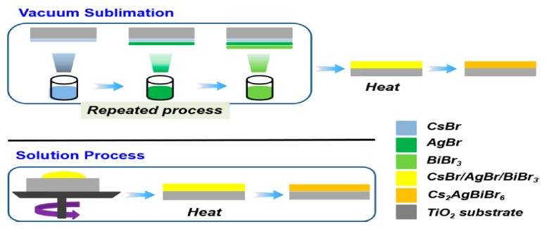
In 2019, Igbari et al. [83] selected two different synthesis methods of solution processing and vacuum processing for preparation of Cs2AgBiBr6 film as shown in Figure 14. The photophysical properties, electronic and crystalline structure as well as photovoltaic properties of the films were compared. The results of various characterizations demonstrated that Cs2AgBiBr6 film prepared by solution processing possessed higher crystallinity, longer charge carrier lifetime, narrower electronic bandgap of 1.98 eV (2.08 eV for vacuum-processed film) and higher mobility compared with vacuum-processed Cs2AgBiBr6 film.
Figure 14.
Preparation sketch of Cs2AgBiBr6 thin film through vacuum-sublimation and solution-processing. Reproduced with permission from [83]. Copyright 2019, American Chemical Society.
2.1.3. Cs2M+Bi3+X6: Doping
Doping/alloying process is an effective method for tuning the electronic properties of the semiconducting materials [89]. For perovskite materials the partial of original constituent elements are replaced by targeted ions which leads to diverse advantages including, enhanced optoelectronic performance, stabilized crystal structure, improvement in photoluminescence properties, etc. [90]. A variety of doped Cs2M+Bi3+X6 structures are reviewed and listed in Table 3. In 2017, Slavney et al. [91] engineered Cs2AgBiBr6 double halide perovskite’s bandgap by dilute alloying Tl+ (Cs2(Ag1−aBi1−b)TlxBr6; 0.003 ˂ x = a + b ˂ 0.075). DFT-PBE+SOC calculations showed that when Ag+ was substituted by Tl+ (x = 0.06), the bandgap would decrease by 0.1 eV with direct transition, while replacing the Bi3+ with Tl3+ (x = 0.06) would lower the bandgap by 0.8 eV and transition would be indirect. Also, doping of 0.075 Tl in (Cs2(Ag1−aBi1−b) TlxBr6 structure decreased the bandgap to 1.40 eV (indirect) or to 1.57 eV (direct). Importantly, the long-lived carrier lifetime in microsecond obtained by time-resolved microwave photoconductivity (TRMC), suggested the efficient extraction of carriers in a solar cell. Both bandgap and carrier lifetime of Cs2(Ag1−aBi1−b) TlxBr6 structure were comparable to MAPbI3 values, but the real setback is that as known Tl+ is toxic.
Table 3.
Summary of prepared doped- Cs-based double halide perovskite samples.
| Compound | Dopant | Morphology | Synthetic Method | Characterization Techniques | Reference |
|---|---|---|---|---|---|
| Cs2(Ag1–aBi1–b) TlxBr6 | Tl+ (0.003 < x < 0.075) | Polycrystalline Powder and single crystals | Solution-based process using hydrohalic acid | TRMC, ICP, Raman, SSRS, XPS, XAS, XANES, SC-XRD, | [91] |
| Cs2Ag (Bi1−xMx) Br6(M = In, Sb) | Sb3+ (x = 0, 0.125, and 0.375) In3+ (x = 0, 0.25, 0.5, and 0.75) |
Powder | Solid-state reaction | PXRD, PL, UV-Vis spectroscopy | [92] |
| Cs2AgInxBi1–xCl6 | In3+ (x = 0, 0.25, 0.5, 0.75, and 0.9) | Nanocrystals | Anti-solvent recrystallization | XRD, TEM, PL, PLQE, HRTEM, TRPL, TCSPC, TA, XPS | [93] |
| Cs2Na1−xBi1−xMn2xCl6 | Mn2+ (x = 0, 0.002, 0.004, 0.012, 0.036) | Polycrystalline | Solution precipitation | PXRD, UV-Vis spectroscopy, EPR, PLQY, TGA, ICP-OES | [94] |
| (Cs1−xRbx)2AgBiBr6 | CsBr:RbBr at 100:0, 95:5, 90:10 and 85:15 | Thin film | Solution-based process | UV-Vis spectroscopy, XRD, PL, IPEC, TRPL, SEM | [84] |
| Cs2NaBiCl6: Ag+, Mn2+, and Eu3+ | Ag+, Mn2+, and Eu3+ | Nanocrystals | Modified hot-injection method | PXRD, TEM, HRTEM, HAADF-STEM, EDS, XPS, UV-Vis spectroscopy, PLQY, ICP-OES, | [95] |
| Cs2AgInCl6: Mn2+ | Mn2+(x = 0%, 0.1%, 0.3%, 0.9%) | Powder | Solution-based process using hydrohalic acid | ICP-AES, FESEM, XRD, TGA, PL, EPR, UV-Vis.spectroscopy, | [96] |
| Cs2AgInCl6: Mn2+ | Mn2+ (x = 0.5% and 1.5%) | Nanocrystals | Colloidal hot-injection method | PL, PLE, PLQY, TRPL, ICP-OES, UV-Vis spectroscopy, TEM, HRTEM, XRD, XPS, ESR, DTA/TG GC-MS | [97] |
| Cs2Ag1−xNaxIn1−yBiyCl6 | Bi3+ and Na1+ (x = 0–1, y = 0.03–0.16) |
Nanocrystals | Room temperature recrystallization process | UV-Vis spectroscopy, TEM, HRTEM, XRD, ICP-OES, PLQY, PL, SEM-EDS, | [98] |
| Cs2AgInCl6: Bi3+ | Bi3+ (x = 0.1%) | Nanocrystals | Facile hot-injection method | XRD, EDS, TEM, HRTEM, UV-Vis spectroscopy, PL, PLE, PLQY | [99] |
| Cs2AgInCl6: Yb3+ | Yb3+ (x = 0.1 to 1.6%) | Microcrystals and Colloidal nanocrystals |
Precipitation method | ICP−AES, ICP−MS, XRD, FESEM, TEM, HRTEM, PL, PLE, TRPL, UV-Vis spectroscopy, TGA, | [100] |
| Cs2NaInCl6: Sb3+ | Sb3+/In3+ (x = 0, 5.0%, 10%, 20%) | Powder | precipitation from an HCl solution | PXRD, TGA, UV-Vis spectroscopy, PLQY, PL, | [101] |
| Cs2NaInCl6: Sb3+ | (Sb/(Sb+In) (x = 0, 5.0%, 10%, 15%, 30%, 60%, 100%) | Powder | Hydrotermal | XRD, UV-Vis spectroscopy, PL, TEM, XPS, PLE, HRTEM, Raman | [102] |
| Cs2Sb1−aAg1−bCu2xCl6 | Cu2+ (a + b = 2x, x = 0.00 (i.e., parent compound), 0.01, 0.05, and 0.10) | Polycrytalline | precipitation from an HCl solution | PXRD, EPR, NMR, ICP-OES, TGA, FESEM | [103] |
| Cs2AgSb1−xBixCl6 | Bi3+ (0 ≤ x ≤ 1) | Nanocrytals | Modified hot-injection method | XRD, FESEM, EDS, TEM, HRTEM, PL, PLE, UV-Vis spectroscopy, | [104] |
| Cs2AgSb1−yBiyX6 (X = Br, Cl) |
Bi3+ (0 ≤ y ≤ 1) | Nanocrytals | Modified hot-injection method | XRD, TEM, PL, Raman, TA, steady-state absorption | [105] |
| Cs2Sn1−xTexI | Te4+(0 ≤ x ≤ 1) | Powder | Solution-phase synthesis | PXRD, UV-Vis spectroscopy, PL, XPS | [106] |
| Cs2SnCl6: Bi | Bi/(Sn + Bi) x = 0%, 0.99%, 4.76%, 9.09%, 13.04%, 16.66%, and 23.08% | Single crystals | Hydrothermal | XRD, ICP-OES, XPS, TGA, UV-Vis spectroscopy, PL, PLQY, PLE, TRPL | [107] |
| Cs2Sn(1−x)GexI6 | Ge4+ (0 ≤ x ≤ 1) | - | - | [108] | |
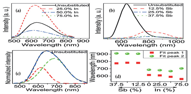
Du et al. [92] through alloying of Sb3+/In3+ in Cs2AgBiBr6 perovskite structure, engineered the bandgap and demonstrated long carrier recombination lifetime. Based on UV-vis diffuse spectra, it was shown that by replacing Bi3+ with In3+, when the level of alloyed metal (x) reach to 0.75 (Cs2AgBi1−xInxBr6), the indirect bandgap would increase to 2.27 eV. On the contrary, substitution of Bi3+ with Sb3+ up to 0.375 (Cs2AgBi1−xSbxBr6; x = 0.375), resulted in narrowing the bandgap from 2.12 eV to 1.86 eV. The opposite bandgap shift direction was related to the different atomic configuration for these metals. The weak PL intensity of In-alloyed sample with high content (x = 0.75) was associated to deeper defect state and symmetry-forbidden transition from valence band to conduction band. Similarly, deep defect state of Sb3+-alloyed sample was responsible for the quickly suppressed emission intensity (Figure 15a–d).
Figure 15.
PL spectra for (a) In-alloyed; (b) Sb-alloyed samples; (c) for Cs2AgBiBr6, fitted using a Gaussian function. Red: fit peak 1, green: fit peak 2, blue dashed line: cumulative fit peak. (d) Fitted PL peak positions as a function of Sb and In alloying ratio. Reproduced with permission from [92]. Copyright 2017, Wiley-VCH.
Cs2AgBi1−xInxCl6 (x = 0, 0.25, 0.5, 0.75 and 0.9) NCs were prepared by Yang et al. [93], through anti solvent recrystallization. In this work, Cs2AgBi1−xInxCl6 (x = 0.25, 0.5) with indirect bandgap were tuned to direct band gap by increasing the In3+ content to 0.75 and 0.9. DFT calculation along with steady-state absorption, PL and transient absorption spectra measurements demonstrated dual color emission of violet (395 nm) (band to band transition) and bright orange (570 nm) (forbidden transition) in NCs.
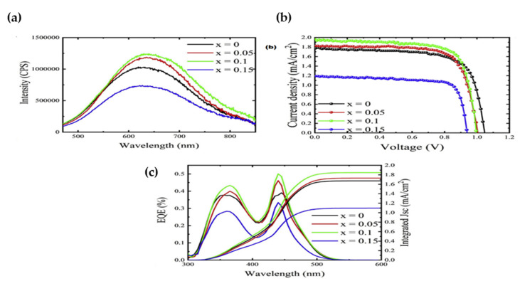
In 2019, Mn2+ doped Cs2NaBiCl6 polycrystalline as a promising orange-red phosphor system was reported by Majher et al. [94]. The absorbed near-UV light by Bi3+ ions in the host lattice transferred to Mn2+ activators and through the spin-forbidden 4T1 → 6A1 transition, light emitting from 525 to 700 nm occurred. Also, they [94] demonstrated partial substitution of Cl− ions by Br− resulted in redshift of exciton spectra as well as an optical absorption peak. Zhang et al. [84], through doping of different amount of Rb+ ion by replacing Cs+ (stochiometric ratio of Cs+/Rb+: 100/0, 95/5, 90/10, 85/15) prepared different (Cs1-xRbx)2AgBiBr6 perovskite compounds. Optical measurements showed with doping ratio of Cs+/Rb+: 90:10, the intensity of PL spectra increased due to the reduction of defects. Moreover, based on IPEC spectrum, it was shown that doping of Rb+ ion leads in enhancement of absorption at longer wavelength as depicted in Figure 16a–c.
Figure 16.
(a) The PL spectra of (Cs1−xRbx)2AgBi6 films on quartz; (b) The J-V curves of the champion devices with (Cs1−xRbx)2AgBi6 and (c) the EQE and IPEC of the devices. Reproduced with permission from [84]. Copyright 2019, Elsevier.
In 2020, Yao et al. [95] reported studies on lead-free double halide perovskite Cs2NaBiCl6 NCs as host, doped with Ag+, Mn2+, Eu3+ ions through hot-injection approach in order to improve the optical properties of the material. The femtosecond time-resolved transient absorption technique was utilized to investigate the PL enhancement mechanism of ion doped NCs. The excitonic absorption energy of Ag-doped sample exhibited red-shift from 3.82 eV to 3.48 eV which led to significant increase of PLQY from 1.7% to 20%. The Mn2+-doped Cs2NaBiCl6 NCs showed a peak centered in 585 nm along with broad red-orange emission owing to 4T1 → 6A1 transition of coordinated Mn2+ ions. Also, Eu3+-doped NCs, owing to the 5D0 → 7FJ (J = 1,2,3,4) transition, demonstrated four sharp emission lines at PL spectra corresponding to 591, 615, 652 and 700 nm, respectively.
2.1.4. Cs2M+Bi3+X6: Applications
Photovoltaic Applications
As presented in Table 2, in 2017, Greul et al. [77] fabricated for the first time the Cs2AgBiBr6-based PSC, which after different parameter measurements exhibited power conversion efficiency (PECs) of 2.43% with Voc exceeding 1 Volt as well as higher stability under constant illumination in ambient environment compared to MAPBI3. In another study, Wu et al. [78] fabricated a PSC with Cs2AgBiBr6 film as active absorbing layer with a PCE of 1.44% and Voc of 1.04 V, Jsc of 1.78 mA cm−2 and FF of 78 under AM1.5 (100 mW cm−2) illumination. The low PCE of the device was attributed to larger exciton binding energy of Cs2AgBiBr6 than MAPbI3. However, the Hole Transporting Layer (HTL)-free device showed higher stability in 4 months compared to MAPbI3 based PSCs.
In 2018, Ning et al. [79] demonstrated the Cs2AgBiBr6 solar cell using one-step spin coating process from single-crystal Cs2AgBiBr6 solution. The device showed a PCE with maximum value of 1.22% and long photoexcited carrier diffusion length close to 110 nm. The Voc of 1.06 V, Jsc of 1.55 mA cm−2 and FF of 74 were also achieved for the device. The low PCE value was attributed to the low efficiency of charge extraction by TiO2 as the electron transporting layer (ETL) as well as presence of interfacial barrier due to the surface defects. They predicated by increasing the film thickness while preserving the quality of the absorber film and replacing the TiO2 by other suitable ETL materials the efficiency of Bi-based halide double perovskite solar cells could be enhanced. Gao et al. [81] adopted anti-solvent dropping methodology for synthesis of Cs2AgBiBr6 film as already shown in Figure 11a,b. The inverted planer heterojunction fabricated device showed PCE of 2.23% with Voc of 1.01 V, Jsc of 3.19 mA cm−2 and FF of 69.2 at forward scan as already depicted in Figure 11d,e. The device also showed good reproducibility, negligible hysteresis and long-term stability. Pantaler et al. [80] reported a hysteresis-free solar device using Cs2AgBiBr6 film as an absorbing layer. In this work, they separately employed three different semiconducting polymers as HTL layer. The best result among different HTL-based devices including spiro-OMeTAD, PCPDTBT (Poly [2,6-(4,4-bis-(2-ethylhexyl)-4H-cyclopenta[2,1-b;3,4-b′]dithiophene)alt4,7(2,1,3-benzothiadiazole)]) and PTAA poly [bis(4-phenyl)(2,4,6-trimethylphenyl)amine), was obtained for PTTA HTL-based device with 1.26% of PCE, 1.02 V of Voc and 1.84 mA cm−2 of Jsc with FF of 67.
In 2018, Zhang et al. [75] replaced Ag+ in Cs2AgBiBr6 double halide perovskite with Na+ ion in order to fabricate the solar device. Cs2NaBiI6 perovskite was prepared by facile one-step hydrothermal process. However, the fabricated device demonstrated low Jsc due to two main reasons, namely that Cs2NaBiI6 perovskite had (1) low hole transport ability, and (2) was not able to efficiently convert the excitons to current. Nevertheless, the fabricated devices showed high stability for 5 months. Testing of a batch of 20 different devices showed the PCE of 0.42% with Voc of 0.47 V, Jsc of 1.99 mA cm−2 and FF of 44. Wang et al. [82] fabricated a PSC by employing sequential-vapor-deposition procedure for synthesis of active layer Cs2AgBiBr6 film as already showed in Figure 13. The device showed lower defect density compered to Cs2AgBiBr6 film prepared by solution process as well as good stability after 240 h under ambient environment. The PCE of 1.37% and Voc of 1.12 V were reported. By employing solution-based processing and vacuum sublimation method, Igbari et al. [83] could achieve an optimized PCE of 2.51% and 1.41%, respectively for Cs2AgBiBr6-based PSCs.
In 2020, Wang et al. [64] studied the performance of Zinc chlorophyll (Zn-Chl) as the HTL in Cs2AgBiBr6-based PSC. It was shown that by employing the Zn-Chl not only enhanced the photovoltaic performance was achieved but also the light absorbing abilities of the Cs2AgBiBr6 through the sensitizing of the perovskite material was improved. The PSCs based on Zn-Chl showed PCE of 2.79% with Voc of 0.99 V, Jsc of 3.83 mA cm−2 and FF of 73.6. In another study in 2020, Yang et al. [65] demonstrated that by employing di-tetrabutylammonium cis-bis(isothiocyanato) bis (2,2′-bipyridyl-4,4′ dicarboxylato) ruthenium (II) (N719) dye as an interlayer on the surface of Cs2AgBiBr6 film, the efficiency and stability of Cs2AgBiBr6-based solar device were boosted. Applying the N719, also led to broadening the light absorption spectrum, reducing the charge carrier recombination, reducing the Cs2AgBiBr6 film surface defects and accelerating the hole extraction. The optimized solar device showed PCE of 2.84% with Voc of 1.06 V, Jsc of 5.13 mA cm−2 and FF of 52.4.
In 2021, Wang et al. [66] following their previous work [64], by employing carboxy-chlorophyll derivative (C-Chl) in the mesoporous TiO2 film, improved the efficiency of Cs2AgBiBr6-based solar cells to more than 3%, which is the highest reported efficiency for Cs2AgBiBr6 PSC. The fabricated PSC based on C-Chl- sensitized mesoporous TiO2 film showed improved PCE of 3.11% with Voc of 1.04 V, Jsc of 4.09 mA cm−2, and FF of 73.
As summarized in this section, Cs2AgBiBr6-based solar cells have showed low power conversion efficiency compared to lead-based PSCs. However, the results obtained show clearly that Cs2AgBiBr6 is a promising material for PV application even though the path to enhance the efficiency might be long. The aforementioned studies [77,78,79,82,84] show that employing of a variety of coating engineering such as using Low-pressure assisted method (LPA), anti-solvent method, vapor deposition method and introducing metal ion dopants resulted in enhanced Cs2AgBiBr6 film morphology improving the efficiency. Furthermore, it was shown that modifying and optimizing ETL and HTL layers also have a significant impact on improvement of efficiency of Cs2AgBiBr6-based solar cells [64,66].
To increase the fill factor (FF) and the open source voltage (Voc), the recombination has to be controlled. It is needed to obtain uniform and high-crystalline perovskite films; meaning that the defect density of the perovskite layer should be reduced [109]. In another words, the higher density traps of the perovskite film cause in more Shockley-Read-Hall (SRH) recombination and lower FF and consequently lead to poor PCE. Wang et al. [66] Used a concept based on ideality factor (N) in order to describe the SRH recombination due to defect density. N is defined by:
where e is electron charge, KB is Boltzmann constant, I is different light intensity, T is the temperature and N shows the charge carrier′ recombination process. For ideal solar cells N must approach unity. When N approaches 2, the performance of the device dominated by Shockley-Read-Hall (SRH) recombination which is assisted by defect density. Therefore, lower N value shows suppression of SRH and reduced trap densities which results in higher fill factor and higher PCE [66].
Non-Photovoltaic Applications
Volonakis et al. [110] adopted first-principle calculation to determine the level of surfaces and surface termination energy of Cs2AgBiCl6, Cs2AgBiBr6, Cs2AgSbCl6 and Cs2AgInCl6 double halide perovskites. Their investigation demonstrated that according to ionization potential and electron affinity, amongst all these four materials, Cs2AgBiCl6 and Cs2AgBiBr6 were the most promising photocatalysts for solar-driven water splitting. Their study also indicated, by increasing the size of halogens in double perovskites, the electron affinity would increase as well, which was due to the shallower energies of the halogen p-states. In 2017, Pan et al. [111] for the first time, reported the application of Cs2AgBiBr6 single crystals as X-ray detectors. Using of thermal annealing and surface treatment resulted in elimination of disordered Ag+/Bi3+ and consequently, the resistivity of the crystals improved. The optimized device showed high sensitivity of 105 μC Gyair−1 cm−2, low detection limit of 105 nC Gyair−1 s−1 under the external bias of 5 V as well as long-term operational stability which all are essential for X-ray detectors in order to medical diagnostics. The single crystals of Cs2AgBiBr6 as suitable semiconductor directly converted X-rays into electrical signals due to its high average atomic number which results in higher X-ray absorption coefficient (α∝Z4 /E3), adequate μτ product (μ = carrier mobility; τ = carrier lifetime), low ionization energy and high resistivity. Yuan et al. [112] by introducing PEABr (phenylethylamine bromide) into the Cs2AgBiBr6 perovskite precursors solution, obtained single crystals of Cs2AgBiBr6 with enhanced ordering degree of [BiX6]3− and [AgX6]5− in octahedra arrangement. The improved order degree gave rise to lower defect density, tunable bandgap, decreased self-trapped exciton formation and increased carrier mobility. The X-ray detector displayed higher current response of 13 vs. 3190 μs, higher sensitivity of 288.8 μC Gyair−1 cm−2 under a bias of 50 μC Gyair−1 cm−2, higher photoconductive gain and longer carrier drift distance. Li et al. [113] synthesized composites films comprised of Cs2AgBiBr6 perovskite embedded in a polymer matrix by a simple drop-casting process. Hydroxyl functional groups of polymers significantly increased the dispersity of Cs2AgBiBr6 in the composite films which led in large area dense films. The fabricated X-ray detector obtained by the composite films demonstrated a sensitivity of 40 μC Gyair−1 cm−2 under the external bias of 400 V, and due to the maximum tolerance of 5% tensile/compressive strain, bending/flexing of detectors did not have any degrading effect on photocurrent.
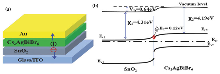
Lei et al. [114] adopted a one-step spin-coating synthesis method for preparation of Cs2AgBiBr6 film as photodetector. The device showed high responsivity of 7.01 A/W, On/Off photocurrent ratio of 2.16 × 10⁴, specific detectivity of 5.66 × 10¹¹ Jones, EQE of 2164%, fast response speed of 956/995 μs. The other remarkable feature of unencapsulated photodetector was the high stability under ambient environment against water and oxygen degradation (36 h continuous operation) without no change in photodetection ability. Wu et al. [115] designed a HTL-free planer heterojunction device including ITO/ SnO2/ Cs2AgBiBr6/Au as ultraviolet (UV) photodetector as shown in Figure 17a,b. The self-powered devices exhibited two responsivity peaks at 350 nm and 435 nm which was associated with ultraviolet-A (320–400 nm). The mechanism explained by separation of photogenerated carriers at the of interface of Cs2AgBiBr6/SnO2 heterojunction by its built-in field. A high responsivity of 0.11 A W−1 at 350 nm and the quick response of less than 3 ms was comparable with other semiconductor oxide heterojunction-based UV detectors. The unencapsulated UV detector also showed remarkable stability under ambient environment for more than 6 months without any noticeable degradation in photocurrent.
Figure 17.
(a) Device configuration diagram and; (b) Band scheme diagram of Cs2AgBiBr6/SnO2 heterojunction. Reproduced with permission from [115]. Copyright 2018, Wiley-VCH.
Zhou et al. [116] reported the fabrication of Cs2AgBiBr6 NCs by hot injection method for CO2 photocatalytic reduction. The prepared double halide perovskite demonstrated significant stability against moisture, light and temperature. It also showed a total electron consumption of 105 μmol g−1 under simulated solar light (AM 1.5G) for 6 h. Zhang et al. [117] developed an alcohol-based photocatalytic system for dye degradation by applying Cs2AgBiBr6 double halide perovskite under visible light irradiation. During the photocatalytic process, Cs2AgBiBr6 kept its high chemical stability in ethanol, and due to the photocatalytic feature of Cs2AgBiBr6 surface, pseudo-zeroth-order kinetics was obtained, and the reaction rate was also comparable to well-known CdS photocatalyst semiconductor.
2.2. Cs/In3+-Based Double Halide Perovskites
2.2.1. Cs2M+In3+X6: Theoretical Results
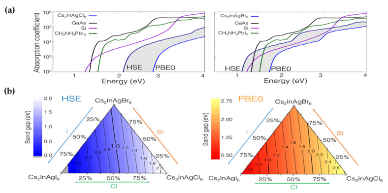
In 2017, Volonakis et al. [118] by using first-principle calculations, identified the direct bandgap of Cs2AgInX6 (X = Cl, Br) halide double perovskites. According to DFT/LDA calculation, In-based perovskites showed smaller lattice constant compared to Bi-Based analogous due to the smaller size of In3+. Preliminary assessment of octahedral and tolerance factor exhibited that because of smaller ionic radii of In3+ (0.8 Å), the coordination between In3+ and I− ions would be impossible, and therefore, the synthesis of Cs2AgInX6 (X = Cl, Br and Cl/Br) double halide perovskite may be amenable. Nominal bandgap for the Cs2AgInCl6 based on theoretical calculation (HSE and PBE0 hybrid functionals) was reported to be of 2.07 eV with a bias of 0.6 eV (Figure 18a,b). They also demonstrated the VBM was mainly comprised of Cl-3p and In-4d/Ag-4d states while the CBM was occupied by Cl-3p and In-5s/Ag-5s states. The electron and hole effective masses were reported to be 0.20 me and 0.28 mh, respectively.
Figure 18.
(a) Calculated absorption coefficient of the synthesized compound, Cs2InAgCl6, and hypothetical compound, Cs2InAgBr6, compared with the theoretical absorption coefficients of Si, GaAs and MAPbI3; (b) Calculated band gaps of hypothetical mixed-halide double perovskites Cs2InAg (Cl1−x−yBrxIy)6 within the HSE (left) and PBE0 (right) hybrid functional. The corners of the triangle correspond to Cs2InAgX6 with X = Cl, Br, I. Reproduced with permission from [118]. Copyright 2017, American Chemical Society.
Zhao et al. [119] as provided in Table 4, inspired by Cu[In,Ga]Se2 (CIGS) chalcopyrite solar absorbers [120,121,122], designed 36 different candidates of double halide perovskites where A = Cs, Rb, K; M+ = Cu, Ag; M3+ = Ga, In and X = Cl, Br, I through first-principles calculations. Although all the compounds showed direct bandgaps, three of them exhibited remarkable bandgap of 1.36 eV (Rb2CuInCl6), 1.46 eV (Rb2AgInBr6) and 1.50 eV (Cs2AgInBr6). Generally, Cu-based compounds showed smaller bandgap than Ag-based perovskites. The screening thermodynamic stability of compounds exhibited positive ∆Hdec that led to suppressed decomposition of compounds. Their study [119] showed that by increasing the film thickness up to 2 μm, spectroscopic limited maximum efficiency (SLME) increased to approximately 28%. This value was attributed to small direct bandgaps of Rb2CuInCl6, Rb2AgInBr6 and Cs2AgInBr6 materials which were close to optimal bandgap of 1.34 eV calculated for Shockley–Queisser limit. This SLME value (28%) was comparable to the obtained SLME values for CuInSe2 (31.5%) and CH3NH3PbI3 (30%).
Table 4.
Summary of prepared double halide perovskite samples based on Cs/In3+.
| Compounds | Morphology | Synthetic Method | Optical Transition | Theoretical Bandgap | Experimental Bandgap | Characterization Techniques | Theoretical Calculation | Reference |
|---|---|---|---|---|---|---|---|---|
| Cs2AgInBr6 | - | - | Direct | 1.50 eV | - | - | DFT/DFT/PBE/HSE | [119] |
| Cs2AgInCl6 | Powder | Solution-based process using hydrohalic acid | Direct | 2.1 ≤ Eg ≤ 3.3 (depends on calculation method) |
3.3 eV | X-ray, UV-Vis spectroscopy, PL, TRPL, | DFT/LDA/HSE/PBE0/HSE | [118] |
| Cs2AgInCl6 | Polycrystalline and single crystals | solid-state reaction and hydrothermal reaction | Direct | 5.0 eV (without SOC) | 3.53 eV | UV-Vis spectroscopy, SC-XRD, PXRD, | DFT-LDA, FP-LAPW+LO, SOC | [125] |
| Cs2AgInCl6 | Nanocrystals | Hot-injection method | Direct | - | 3.57 eV | STEM-EDS, UV-Vis-NIR spectroscopy, PL, PLE, TEM, XRD | DFT-VASP, PBE-GGA | [85] |
| Cs2AgInCl6 | Powder | Hydrothermal method | Direct | 3.33 eV | 3.23 eV | TRPL, UV-Vis, XRD, SEM, UV-Vis spectroscopy, PL, TGA | DFT/PAW/PBE/VASP | [124] |
| Rb2AgInBr6 | - | - | Direct | 1.46 eV | - | - | DFT/DFT/PBE/HSE | [119] |
| Rb2CuInCl6 | - | - | Direct | 1.36 eV | - | - | DFT/DFT/PBE/HSE | [119] |
The intrinsic defects of In-based double halide perovskite were investigated by Xu et al. [123] through the first-principle calculation. The theoretical study of band structure showed hybridization of Ag(d) and ionic X(p) orbitals along with negligible coupling with In (s) orbital resulted in direct bandgap where both VBM and CBM were placed at Γ point of Cs2AgInCl6. It was expected that Cs2AgInCl6 shows more point defects as a quaternary compound, which makes the growth of high-quality film challenging. It was shown that in order to avoid of deep-level defects and unwanted secondary phases, the synthesis of film should be done in Ag-rich growth condition. It was also suggested that depending on chemical growth condition, the conductivity of Cs2AgInCl6 could change from good n-type/poor n-type to intrinsic semiconducting.
2.2.2. Cs2M+In3+X6: Experimental Results
Cs2M+In3+X6: Single-Crystals, Polycrystalline and Nanocrystals-Based Perovskites
In order to verify the accuracy of theoretical studies on stability, direct bandgap and balanced effective masses of Cs2AgInX6 (X = Cl, Br) Volonakis et al. [118] synthesized the materials through precipitation from the acid solution. The experimental measurements were in a good agreement with their theoretical results. The optical bandgap obtained by experimental measurements was 3.3 eV as presented in Table 4.
Zhou et al. [124] synthesized Cs2AgInCl6 perovskite crystals by using hydrothermal method. The size of the crystals varied between 5 to 15 μm which was due to the different reaction time. Rietveld analysis for XRD measurement of Cs2AgInCl6 powder identified the cubic unit cell with the space group of Fm-3m [AgCl6] and [InCl3] octahedra in 3D framework. Time-resolved emission spectra showed two different decay times of 16.3 and 100 μs which was attributed to surface/defect states and fundamental nonradiative recombination. The optical bandgap measured by UV-vis reflectance spectroscopy was 3.23 eV while this value determined to be 3.33 eV by using band structure and optical absorption calculations. However, the compound showed to maintain high light, moisture and heat stability.
2.2.3. Cs2M+In3+X6: Doping
In 2018, Nag et al. [96] prepared bulk Mn-doped Cs2AgInCl6 perovskite employing the same method used by Volonakis et al. [118] in order to study the photoluminescence properties. The optical measurements of samples showed a weak intensity of undoped sample while by increasing of Mn2+ concentration as dopant, the intensity of emissions raised up significantly. This was due to the de-excitation of Mn2+ d-electrons from 4T1 → 6A1 state. Locandi and co-workers [97] prepared Cs2AgInCl6 and Mn-doped Cs2AgInCl6 NCs, using colloidal hot-injection method. Synthesis resulted in highly pure NCs without any undesired secondary phases for both Cs2AgInCl6 and Mn-doped Cs2AgInCl6 as well as high thermal stability up to 500°. The experimentally obtained optical bandgap was larger compared to previously reported works (4.38 eV for Cs2AgInCl6 NCs and 4.36 eV for Mn-doped Cs2AgInCl6 NCs). However, the Mn-doped Cs2AgInCl6 NCs exhibited bright PL emissions with a PLQY of 16 ± 4% which is comparable to Cs2AgInCl6 NCs value (1.6 ± 1%). This result shows that doping with Mn2+ would make the In3+-based double halide perovskites a good candidate for different applications such as LEDs.
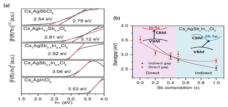
Tran et al. [125] through a solid-state technique synthesized Cs2AgInCl6 while the Cs2AgSbxIn1−xCl6 (x = 0.5, 0.4 and 0.2) solid solutions were prepared by combining the single crystals of hydrothermally synthesized of Cs2AgInCl6 and Cs2AgSbCl6, in a stoichiometric ratio. UV-Vis diffuse reflectance measurement along with Tauc plot demonstrated, by increasing the Sb composition in Cs2AgSbxIn1−xCl6 (x = 0.5, 0.4 and 0.2 and 0), the bandgap would shift from direct to indirect while the value decreased from 3.53 eV to 2.54 eV in Cs2AgSbCl6 (Figure 19a,b).
Figure 19.
(a) Tauc plots for Cs2AgSbCl6, Cs2AgSb0.5In0.5Cl6, Cs2AgSb0.4In0.6Cl6, Cs2AgSb0.2In0.8Cl6 and Cs2AgInCl6. The plots indicate the characteristics of an indirect bandgap for Cs2AgSbCl6, a direct bandgap for Cs2AgInCl6 and a transition from indirect to direct bandgap of Cs2AgSbxIn1−xCl6 at x = 0.4; (b) Phase diagram of Cs2AgSbxAg1−xCl6 showing the bandgap trend as a function of Sb composition and a crossover from indirect to direct optical absorption in a solid solution at x = 0.4. Reproduced with permission from [125]. Copyright 2017, Royal Society of Chemistry.
Liu et al. [99] by utilizing a facile hot injection method, prepared Cs2AgInCl6 and Bi-doped Cs2AgInCl6 NCs. It was indicated that by controlling the reaction time both ligands and HCl concentration, the purer NCs without any impurity phases with desirable size and shapes would be produced. By increasing the reaction temperature from 180° to 280°, the PLQY curve also rise and reached to highest PLQY of 11.4%. TEM and HRTEM analysis of NCs formed at 180° exhibited of some spherical particles which were ascribed to Ag2O. Due to metal-ion-induced oxidation process the silver ions turn to silver nanoparticles. The size of undoped and doped (with 1% Bi3+ ions) NCs were reported 9.79 nm and 10.59 nm, respectively. The optical measurements of NCs revealed a broad orange peak at 580 nm for Bi-doped Cs2AgInCl6 and a blue emission peak at 470 nm for Cs2AgInCl6. It was also indicated that by doping Bi3+ in Cs2AgInCl6 NCs, the number of defects would decrease, and radiative localization would be promoted. The long-life time and broadened emission of Bi-doped Cs2AgInCl6 NCs were attributed to self-trapped excitation (STEs) stemming from the Jahn-Teller distortion of [AgCl6] octahedron in the excited state as well as the trivial sub-bandgap defect state transition.
In 2019, Hu et al. [98] prepared colloidal Cs2Ag1−xNaxIn1−yBiyCl6 (x = 0–1; y = 0.03–0.16) NCs by a room temperature recrystallization process. The mean size of NCs were reported to be of 3 nm with diameter of 1.8–4.0 nm which could potentially confine the excitons. The remarkable blueshift photoluminescence was observed for the NCs which was comparable for bulk materials. Incorporation of partial amount of Na+ and Bi3+ resulted in bright near-white light emission with tunable color temperatures from 9759.7 to 4429.2 K. Furthermore, the introduction of Bi3+ ions along with OA (ligand) passivation in Cs2Ag0.17Na0.83In0.88Bi0.12Cl6 nanocrystals led in PLQY of 64% which was the highest reported value for lead-free NCs to date.
In order to investigate the geometric, electric and photoluminescence properties of Mn2+-doped Cs2AgInCl6 double halide perovskite, Wu et al. [126] employed first-principle calculations. Their study showed that the presence of Mn as a dopant resulted in defect complexes by replacement of Ag+ with Mn2+ atom and causing Ag vacancy (MnAg VAg), which was due to the charge balance and weak distortion of the metal octahedra. Subsequently, this defect configuration introduced two defect bands in the forbidden gap which was associated to 3d orbitals of the Mn2+ ions. Therefore, the transition of electron from the first excited state to the ground state led to lower PL spectrum compared to bandgap which would make it beneficial for LEDs.
In 2019, in order to tune the bandgap of Cs2AgInCl6, microcrystal and colloidal nanocrystals of Yb3+ doped Cs2AgInCl6 were prepared by Mahor et al. [100] through the solution-process and hot-injection methods, respectively. The concentration of Yb3+ content, analyzed by Inductively coupled plasma mass spectrometry (ICP-MS) was reported to have 0.1–1.6% for microcrystals and 6.2% for NCs. The Yb-doped samples showed an intense NIR emission centered at ~994 nm. Optical measurements of the samples indicated the light at first was absorbed by the light and then non-radiatively transferred to excite the Yb3+ ions and resulted in the de-excitation of (f) electrons in Yb3+ ions (2F5/2 → 2F7/2). However, the PL decay was different for microcrystals compared to nanocrystals doped perovskites. The NCs exhibited a biexponential decay of 3 ms and 749 μs, and the microcrystals showed a single-exponential decay of Yb-emission with a lifetime of 2.7 ms. The samples also showed high stability under ambient environment.
In 2020, the Pb-free double halide perovskite Cs2NaInCl6:Sb3+ was prepared by Gray et al. [101] through precipitation from an HCl solution with the aim of photoluminescent properties investigation. The PXRD analysis of doped and undoped compounds indicated Fm-3m crystal symmetry, a = 10.553344(4) Å with rock salt fully ordering of In3+ and Na3+ ions sites. The compound showed a large bandgap of ~5.1 eV. However, the substitution of In3+ with Sb3+ resulted in strong absorption in the UV because of 5s2 → 5s15p1 transitions of [SbCl6]3−. Through the transition from 3P1 → 1S0 with radiative relaxation back to 5s2 ground state, strong blue luminescence at 445 nm with a PLQY of 79% was observed. Nevertheless, with increasing of Sb3+ content in Cs2NaInCl6, more than 3% the PL intensity decreased. Furthermore, Cs2NaInCl6:Sb3+ showed smaller Stocks shift (0.94 and 1.38 eV) compared to vacancy ordered double perovskite Cs2SnCl6, which was due to the change of coordination number from 6 in Cs2NaInCl6 to 5 in Cs2SnCl6.
In a similar study, Zeng et al. [102] showed that doping of 10% Sb3+ in Cs2NaInCl6 perovskite would break the parity forbidden transition as well as modulating of density of state (DOS) population which led to an optimized blue PLQY of 78.9% assigned to be self-trapped excitons (STEs).
2.2.4. Cs2M+In3+X6: Applications
Non-Photovoltaic Applications
In 2017, Luo et al. [127] fabricated single crystals of Cs2AgInCl6 by thermodynamic synthesis method for UV photodetection. The prepared single crystals showed light yellow color on surface with colorless interior. This phenomenon was explained by different compositions of sample which means oxygen or oxygen containing functional groups change the surface compositions, consequently the optical properties of sample would change. Furthermore, the optical measurements of sample verified the existence of parity-forbidden transition in Cs2AgInCl6, which had been already demonstrated by Yan et al. [53] through theoretical calculation. It was suggested that the large difference between experimentally obtained optical bandgap (3.2 eV) and photoluminescence emission energy (2.1 eV) was caused by parity-forbidden transitions. However, the fabricated UV photodetection device exhibited ultralow trap-density of 8.6 ± 1.9 × 108 cm−3 which was comparable with Pb-based perovskites value (1.80 ± 1.07 × 109 cm−3), as well as high ON-OFF ratio of around 500, fast photo response of 1 ms, low dark current of 10 pA at 5 V bias and high detectivity of 1012 Jones.
Co-doped Cs2AgInCl6: Bi3+-Ln3+ (Ln3+ = Er3+ and Yb3+) perovskite, with the aim of improving both absorption and emission spectra of the Cs2AgInCl6 were prepared by Arfin et al. [128]. Their study showed that co-doping of Bi3+ in Cs2AgInCl6 along with Ln3+(Ln3+ = Er3+ and Yb3+) resulted in new optical absorption channel in a lower energy (372 nm), which is appropriate for excitation in commercial UV LEDs. This excited energy gets effectively transferred to f-electrons of Er3+ or Yb3+ ions leading to emission at 1540 nm and 994 nm, respectively and generally improve the near infrared (NIR) dopant emissions. Moreover, excitation at lower energy led to that co-doped Bi3+-Er3+: Cs2AgInCl6 exhibited 45-times higher emission intensity and co-doped Bi3+-Yb3+: Cs2AgInCl6 showed 27-times higher emission intensity compared to single doped Er3+: Cs2AgInCl6 and Yb3+: Cs2AgInCl6 compounds.
2.3. Cs/Sb3+-Based Double Halide Perovskite
2.3.1. Cs2M+Sb3+X6: Theoretical Results
In 2017, Tran et al. [125], as presented in Table 5, exhibited a new design for engineering the convergence of direct and indirect bandgap in double halide perovskites based on chemical adjustment of (s) and (p) orbitals character in CBM. Because of differences in orbital overlaps, the relative crystals momenta of VBM and CBM determine whether a bandgap is direct or indirect. This means that bands derived by s-orbitals will increase in energy from Γ to X in a cubic Brillion zone while the bands derived by p-orbitals reduce in energy. Therefore, if the conduction band can be adjusted from s orbitals to p orbitals with a negligible change in the valance band consequently, the difference would result in shift from direct to indirect bandgap. By means of this theory, they examined the feasibility of their design strategy with the experimental preparation of Cs2AgInCl6, Cs2AgSbCl6 and Cs2SbxIn1−xCl6 (x = 0.5, 0.4 and 0.2). Their experimental study successfully demonstrated that Cs2AgInCl6 and Cs2AgSbCl6 showed direct and indirect bandgaps, respectively. By employing the optimized amount of 60%: 40% for In3+: Sb3+ in Cs2SbxIn1−xCl6, it was shown that the bandgap changes from indirect to direct.
Table 5.
Summary of prepared double halide perovskite samples based on Cs/Sb3+.
| Compound | Morphology | Synthetic Method | Optical Transition |
Theoretical Bandgap |
Experimental Bandgap |
Characterization Techniques |
Theoretical Calculation |
Reference |
|---|---|---|---|---|---|---|---|---|
| Cs2AgSbBr6 | Single crystals and thin film | Hydrothermal and Solution-based process using hydrohalic acid | Indirect | 1.46 eV | 1.64 eV for crystals 1.89 eV for mixed-phase film |
XRD, XPS, UV-Vis spectroscopy, XRF |
DFT/PAW/VASP, HSE06+SOC, QTAIM/ CRITIC2 | [62] |
| Cs2AgSbBr6 | Polycrystalline | Mechanochemical | Indirect | - | 1.93 eV | XRD, XPS, UV-Vis spectroscopy, TG-DSC, TCSPC, XRF | - | [63] |
| Cs2AgSbCl6 | Polycrystalline and single crystals | Solid-state reaction and hydrothermal reaction |
Indirect | 2.4 eV | 2.54 eV | UV-Vis spectroscopy, SC-XRD, PXRD, | DFT-LDA, FP-LAPW+LO, SOC | [125] |
| Cs2AgSbCl6 | Crystals | Hydrothermal | Indirect | 2.35 eV (by HSE) 1.40 eV (by PBE) |
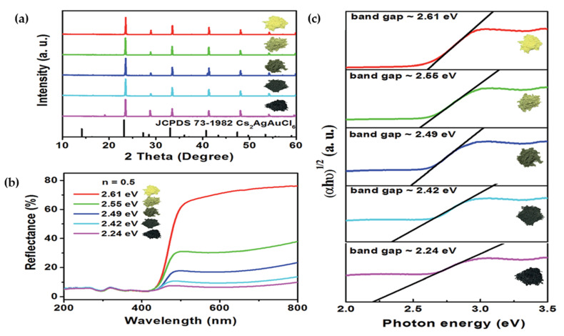
2.24 eV ≤ Eg ≤ 2.61 eV (depends on HCl amount) |
XRD, UV-Vis-NIR spectroscopy, SEM, TG-DSC | DFT-VASP, PAW, GGA-PBE, HSE | [124] |
| Cs2AgSbCl6 | Nanocrystals | Hot-injection method |
Indirect | - | 2.53 eV without AgCl 2.57 eV with AgCl |
STEM-EDS, UV-Vis-NIR spectroscopy, PL, PLE, TEM, XRD, | DFT-VASP, PBE-GGA | [85] |
| Cs4CuSb2Cl12 | Polycrystalline | Solution-based process using hydrohalic acid | Direct | 0.98 eV by Dmol3 1.63 eV by CASTEP 2.44 eV by VASP |
1.02 eV | PXRD, TGA, UV-Vis-NIR spectroscopy, UV stability test, SC-XRD | DFT/Dmol3/CASTEP/VASP | [129] |
| Cs4CdSb2Cl12 | Single crystals | Solvothermal | Direct forbidden |
3.29 eV | 3.0 eV | PXRD, SC-XRD, TGA, EDS, PL, PLE, TRPL, UV-Vis-NIR spectroscopy | DFT/VASP/PAW, GGA-PBE, HSE+SOC | [68] |
Zhou et al. [130] investigated the color-tuning phenomenon of Cs2AgSbCl6 crystals which occurred during the synthesis procedure by PBE approaches through first-principle calculation while anti-site defect was established as a model. It was shown that with exchanging site-equal Ag and Sb ions, the two allotropes of nearest neighbor (NN) and second nearest neighbor (2NN) were stable with only 7–12 meV per atom larger than balanced structure (Ebalanced > ENN > E2NN), and the relatively small lattice expansion resulted in different bandgaps.
In 2019, Wei et al. [62] investigated the crystallinity and symmetry of Cs2AgSbBr6 double halide perovskites by employing DFT calculations. It was shown that even though there was a similarity between band structure of Cs2AgSbBr6 and Cs2AgBiBr6, the 5s 5p orbitals in Sb lowered the CBM significantly, which led to smaller bandgap in Cs2AgSbBr6 compared to Cs2AgBiBr6. Lin et al. [68] presented a strategy for developing quadruple perovskite halides. Through DFT calculations and symmetry analysis, Cs4CdSb2Cl12 and Cs4CdBi2Cl12 were identified as two stable perovskites with vacancy ordered 3D crystal structure along with 3D electronic dimensionality with direct forbidden bandgaps.
2.3.2. Cs2M+Sb3+X6: Experimental Results
Cs2M+Sb3+X6: Single-Crystals, Polycrystalline and Nanocrystals-Based Perovskites
Zhou et al. [130] hydrothermally synthesized Cs2AgSbCl6 crystals and demonstrated by increasing the amount of HCl as a solvent from 0.5 to 1.5 mL, the color of prepared powders changed from yellow to near black, which directly influenced on bandgap. While the darker samples showed lower bandgaps and the lighter color samples indicated higher bandgap as depicted in Figure 20a–c.
Figure 20.
(a) XRD pattern; (b) UV-vis diffuse spectra and; (c) Tauc plots of as-synthesized Cs2AgSbCl6 samples obtained by employing of different amounts of HCl (0.5, 0.75, 1.0, 1.25 and 1.5 mL) with variable visible light absorbance. Reproduced with permission from [130]. Copyright 2018, Royal Society of Chemistry.
Vargas et al. [129] by incorporation of Cu2+ and Sb3+ through a solution method, prepared a 2D layered double halide perovskite, Cs4Sb2CuCl12, which exhibited a promising direct bandgap of around ~1 eV, due to the unpaired electron in the 3d orbital of Cu2+. The crystalline structure of the perovskite comprised of [CuCl6]4− octahedra which was placed between [SbCl6]3− layers and corner-shared to [SbCl6]3− octahedra. The prepared perovskite showed high stability against moisture, light and temperature.
In 2019, Wei et al. [62] prepared a bulk form of Cs2AgSbBr6 double halide perovskite through the hydrothermal method. The prepared samples showed a low indirect bandgap of 1.64 eV for single crystals. The color of as-prepared samples changed from black to brown by increasing the temperature to 480 K for 5 min, which could be ascribed to charge transfer between Sb3+ and Sb5+ in a black phase.
Dahl et al. [85] synthesized Cs2AgSbCl6 and Cs2AgInCl6 nanocrystals by using a modified hot injection method. Instead of adding cesium oleate which is regularly used in the synthesis of double halide perovskites acyl halides was added into the solution of metal acetate precursors under ambient environment at mild temperatures. It was found that the concentration and type of acyl halide had a deep effect on synthesized nanocrystals. The prepared crystalline nano-cubes showed an edge length of 10 nm terminated with (200) facets as well as small silver nano-crystallites decorating the cubes. By developing a titration essay, in order to test the stability of prepared NCs, Dahl et al. [85] observed that Cs2AgSbCl6 dissolved in the presence of minimum concentration (0.01–0.1 mM) of octylamine and released more than twice decomposition energy compared to Cs2AgInCl6 and CsPbCl3 as illustrated in Figure 21a,b.
Figure 21.
(a) reaction sketch for the preparation of double halide Cs2AgSbCl6, Cs2AgInCl6 and Cs2AgBiCl6 perovskite NCs. A solution of metal acetates (cesium, silver and indium, antimony or bismuth) in xylene with oleic acid and oleylamine is heated to 100 °C, then an acyl chloride precursor is injected to form NCs of the corresponding Cs2AgMCl6 (M = In, Sb, Bi) double perovskite. The reactivity of the acyl chloride precursor is an important factor for tuning nanocrystal formation; (b) analysis of stability for Cs2AgSbCl6, Cs2AgInCl6 and Cs2AgBiCl6 and CsPbCl3 NCs. Individual points represent the fraction of initial absorption remaining after 4 h as a function of the different concentrations of octylamine that the nanocrystal solutions were exposed to. Reproduced with permission from [85]. Copyright 2019, American Chemical Society.
Lin et al. [68] synthesized Cs4CdSb2Cl12 and Cs4CdBi2Cl12 3D perovskites by solvothermal method in order to support their theoretical results. The steady-state PL exhibited warm orange emission, while the transient PL showed carrier recombination lifetime of microseconds at low temperature.
Garcia-Espejo et al. [63] by employing a mechanochemical approach, prepared polycrystalline inorganic Cs2AgSbBr6 double perovskites. Bromide derivative salts were added to a high energy ball mill with different molar ratio under atmospheric condition. Due to the thermodynamic instability of Cs2AgSbBr6, XRD for Cs2AgSbBr6 showed varied X-ray diffraction peaks showing the formation of side phases such as AgBr, CsAgBr2 and Cs3Sb2Br9. It was demonstrated that 2D layered of Cs3Sb2Br9 is more stable than 3D Cs2AgSbBr6 double perovskite [131]. The Cs2AgSbBr6 bandgap from Tauc plot was estimated to be 1.93 eV.
Deng et al. [132] integrated Cs2AgSbCl6 powder and Cs2AgSbCl6/TiO2 heterojunction nanoparticles through solution state method and hydrothermal process, respectively. Optical bandgaps of 2.60 eV from optical absorption curve for Cs2AgSbCl6 were obtained. However, the optical absorption was seen improved for Cs2AgSbCl6/TiO2 heterojunction sample in the visible region as a result of interface states formation and lowered bandgap showing the facilitation of the photo-induced optical transitions. The comparison of charge transfers of Ag2Sb2Cl8/TiO2 and Cs4Cl4/TiO2 indicated that photo-induced carrier separation was more efficient at Cs4Cl4/TiO2 interface.
2.3.3. Cs2M+Sb3+X6: Doping
Tran et al. [125] through the solid-state technique synthesized Cs2AgSbCl6 perovskite and Cs2AgSbxIn1−xCl6 (x = 0.5, 0.4 and 0.2) were prepared by combining the single crystals of hydrothermally synthesized Cs2AgInCl6 and Cs2AgSbCl6 in a stoichiometric ratio. UV-Vis diffuse reflectance measurement along with Tauc plot demonstrated that by increasing the Sb composition in Cs2AgSbxIn1−xCl6 (x = 0.5, 0.4 and 0.2 and 0), the bandgap would shift from direct to indirect while the value decreased from 3.53 eV to 2.54 eV in Cs2AgSbCl6.
Karmakar et al. [103] by investigating of Cs2AgSbCl6 and Cu2+-doped Cs2AgSbCl6 double halide perovskites reported of a well- ordered crystal structure with integration of Cu2+ ions into the lattice where Ag+ ions were replaced by Cu2+. The results of optical measurements showed that Cu2+ ions had a direct effect on reduction of bandgap from 2.56 eV (Cs2AgSbCl6) to 1.02 eV for Cu-doped Cs2AgSbCl6 (x = 0.1 Cu2+). The prepared Cu-doped Cs2AgSbCl6 perovskite exhibited significant stability up to 365 days. The DFT calculation demonstrated small carrier effective masses (>0.4 me). Furthermore, it was found that using Cu2+ ion as dopant increased the conductivity of semiconductor. Kshirsagar et al. [104] prepared Cs2AgSb1−xBixCl6 alloy NCs with 0 ≤ x ≤ 1 by employing the hot-injection method. Incorporation of Bi3 in Cs2AgSb1-xBixCl6 NCs (x = 0.36) raised the PL emission intensity to the maximum level of 2.74 eV. Also, a broadened red-shift emission was observed at 2.17 eV which was ascribed to the carrier-phonon coupling leading intrinsic self-traps. The average length of 10 nm was characterized by TEM images, which proved that even with incorporation of Bi, the size and shape of NCs remained unchanged. The absorption spectra of Cs2AgSbCl6 exhibited an absorption peak at 3.45 and 4.08 eV. Since the edge length of synthesized NCs were larger than Bohr radius (1.02 nm), and due to the absence of quantum confinement effect in NCs, no modifications in absorption spectrum were observed. However, the addition of Bi in Cs2AgSb1−xBixCl6 (x = 1), decreased the bandgap from 3.45 eV to 3.39 eV as a result of larger spin-orbit coupling strength of Bi as well as anti-site disorders as shown in Figure 22a,b.
Figure 22.
(a) UV-vis absorption and; (b) PL spectra after excitation at 310 nm for colloidal Cs2AgSb1−xBixCl6 alloy NCs. The samples in (a) all were normalized at 3.4 eV which is the lowest energy peak. Reproduced with permission from [104]. Copyright 2019, American Institute of Physics.
2.3.4. Cs2M+Sb3+X6: Applications
Photovoltaic Applications
To the best of our knowledge, there have not been any significant studies on Sb3+-based double perovskite for PV application. The only fabricated PSC based on Cs2AgSbBr6 thin film was reported by Wei et al. [62] in 2019 with a very low photovoltaic efficiency (0.01%), which was attributed to the presence of secondary phases with large bandgaps.
2.4. Cs-Based Vacancy-Ordered Double Halide Perovskites
Vacancy-ordered double perovskites are another form of double perovskite in which one B-site cation is replaced by a vacancy and the other B-site cation is in a oxidation state of B4+ (A2M1+M3+X6 → A2□M4+X6 → A2M4+X6; where □ indicates a vacancy). This category of perovskite materials also has the close-packed anionic lattice like ABX3. While in ABX3 structure, the stability of the perovskite is predicted by Goldschmidt tolerance factor, in A2BX6 structures the radius ratio is calculated by A-site cation radius to the 12-coordinate void [133,134,135,136] as shown in Figure 23a,b.
Figure 23.
(a) Crystal structure of the vacancy-ordered double Cs2SnI6 and Cs2TeI6 perovskites; (b) Reorientation of the unit cell reveals the isolated octahedral units. Reproduced with permission from [136]. Copyright 2016, American Chemical Society.
2.4.1. Cs2M4+X6: Theoretical Results
In 2014, Lee et al. [137], as provided in Table 6, investigated the band structure of perovskite by DFT calculations and it was shown that Cs2SnI6 possessed a direct bandgap of 1.3 eV at the Γ point comprised of filled I-5p and empty I-6p/Sn-5p orbitals which contributed to VBM and CBM, respectively. Both VBM and CBM were dispersed in energy resulting in high charge carrier mobility of Cs2SnI6.
Table 6.
Summary of prepared vacancy-ordered double halide perovskite samples.
| Compound | Morphology | Synthetic Method | Optical Transition | Theoretical Bandgap | Experimental Bandgap | Characterization Techniques | Theoretical Calculation | Reference |
|---|---|---|---|---|---|---|---|---|
| Rb2SnI6 | Powder | Solution precipitation | Direct | 1.13 eV and 1.32 eV (depend on the calculation) | 1.32 eV | XPDF, nPDF, UV-Vis spectroscopy, PPMS, SXRD, PXRD | DFT-VASP, PAW, PBEsol, HSE06, HSE06+SOC, DFPT | [106] |
| Cs2AuI6 | - | - | Direct | 1.31 eV | - | - | DFT-VASP, PAW, PBE, HSE | [138] |
| Cs2TiBr6 | Powder | melt-crystallization method | Indirect | 2.01 eV (HSE) 1.89 eV (HSE+SOC) |
1.78 eV | UV-Vis spectroscopy, XRD | DFT-VASP, PAW, HSE06 | [139] |
| Cs2TiI2Br4 | Powder | melt-crystallization method | Indirect | 1.49 eV (HSE) 1.32 ev (HSE+SOC) |
1.38 eV | UV-Vis spectroscopy, XRD | DFT-VASP, PAW, HSE06 | [139] |
| Cs2TiI6 | Powder | melt-crystallization method | Indirect | 1.20 eV (HSE) 1.05 eV (HSE+SOC |
1.02 eV | UV-Vis spectroscopy, XRD | DFT-VASP, PAW, HSE06 | [139] |
| Cs2TiI4Br2 | Powder | melt-crystallization method | Indirect | 1.10 eV (HSE) 1.00 eV (HSE+SOC |
1.15 eV | UV-Vis spectroscopy, XRD | DFT-VASP, PAW, HSE06 | [139] |
| Cs2Ti (BrxCl1−x)6 (0 < x < 1) | Powder | Solution-based process using hydrohalic acid | Quasi-direct | ∼1.6 eV to ∼2.3 eV | ∼1.7 eV to ∼2.5 eV | SEM, EDS, XRD, TGA, UV-Vis-NIR spectroscopy, PL, PLQY | DFT-CASTEP, GGA-PBE | [141] |
Maughan et al. [106] through DFT calculations indicated that the phonon interaction was stronger in Rb2SnI6 compared to Cs2SnI6. This was caused by the larger number of nondegenerate lower frequency phonons which contributed to the lattice dielectric response and decreased charge carrier mobilities. Debbichi et al. [138] theoretically studied the atomic and electronic band structures of single crystal and polycrystal Cs2Au2I6. It was shown that Au demonstrated mixed-valence of +1 and +3 in the B-site, which made the Cs2Au2I6 to exhibit the same electronic structure as double perovskite materials resulting in an optimal bandgap of 1.31 eV. An in-depth optical simulation done by Debbichi et al. [138] suggested that polycrystalline Cs2Au2I6 would be a good candidate for PV application because of its remarkable optical absorption and electrical performance such as small effective masses and long diffusion length. It was predicted by employing polycrystalline Cs2Au2I6 as an active layer in PSC, the short-circuit-current of 30 mA cm−2 and photoconversion efficiency of 20% could be obtained. They used full-wave electromagnetic simulations based on the finite element methods (FEM) to do their calculation.
In 2017, Ju et al. [139] introduced a new class of vacancy-ordered perovskite based on Ti4+ ion. Their experimental and theoretical results indicated that both Cs2TiI2Br4 and Cs2TiBr6 possessed the ideal bandgap values of 1.38 eV for single junction and 1.78 eV for tandem solar cells. Moreover, both materials exhibited good environmental stability. Sakai et al. [140], by employing DFT/GCA calculations showed that the electron and hole effective masses of Cs2PdBr6 were to be 0.53 and 0.85 me, respectively, which resulted in n-type semiconductivity in Cs2PdBr6.
2.4.2. Cs2M4+X6: Experimental Results
Cs2M4+X6: Single-Crystals, Polycrystalline and Nanocrystals-Based Perovskites
Lee et al. [137] prepared Cs2SnI6 perovskite as a stable molecular iodosalt serving as a hole transporting layer in solid-state DSSCs. This iodosalt compound which Sn is on its +4-oxidation state showed high stability against moisture and air compared with CsSnI3 and MASnI3 perovskites.
In 2019, Kong et al. [141] adopted a solution-based process for synthesis of Cs2TiX6 (x = Cl and Br) at room temperature. The highly uniform and thermally stable crystals and thin film of Cs2TiBrxCl1−x (0 < x < 1) were prepared. The obtained materials showed a quasi-direct bandgap of 1.7 eV for Cs2TiBr6, 1.95 eV for Cs2TiBr2Cl4 and 2.5 eV for Cs2TiCl6. Furthermore, steady-state PL exhibited an emission peak centered at ~535 nm for Cs2TiCl6, ~635 nm for Cs2TiBr2Cl4 and ~670 nm for Cs2TiBr6. The FWHM values for all prepared samples were larger than 100 nm, which is comparable with Pb-based perovskites. However, in order to obtain more efficient thin films and for engineering the bandgaps, they suggested different synthesis approaches and alloying with other metallics or halide elements were required. Sakai et al. [140] by employing the solution process technique, synthesized Cs2PdBr6 halide perovskite. During the synthesis process, the oxidation state of Pd2+ changed to Pd4+ which was generated in situ. The obtained compound crystallized in a cubic structure with a space group of fm-3m. The optical measurements indicated that compound had an indirect bandgap of 1.6 eV. In order to study the sample photoconductivity a sandwich structure was fabricated including ITO/Cs2PdBr6/Ag. The carried-out experiment confirmed the feasibility of Cs2PdBr6 perovskite for different optoelectronic applications such as LEDs, PV and photon-sensors.
Cs2M4+X6: Film-Based
Chen et al. [87], as already presented in Table 2, by employing the facile low-temperature vapor deposition methodology, prepared a high-quality thin film of Cs2TiBr6 halide perovskite. The synthesized thin film demonstrated an optimal bandgap of 1.78 eV with a carrier diffusion length of more than 100 nm.
2.4.3. Cs2M4+X6: Doping
In 2016, the solid-solution of Cs2Sn1−xTexI6 was prepared by Maughan et al. [136] in order to investigate of its structure-property relationship. The substitution of Sn by Te causing the increase of electronic dispersion due to the closer contact distances of I-I bonding resulted in reduction of conductivity, carrier mobility and carrier concentration. DFT calculation revealed the hindered formation of intrinsic iodine vacancy donor defects resulting in insulating characteristics of Cs2TeI6. However, the theoretical calculation of Cs2SnI6 native defects showed a low enthalpy of iodine vacancies formation and a level of defect energy that was a shallow donor to the conduction band. This makes the material tolerant to defect states. In Te-doped compound, the covalency of Te-I bonding suppresses the formation of iodine vacancy state causing the reduction in conductivity.
Maughan et al. [106] studied the electrical and structural changes created by substitution of Cs+ with Rb+. Both Cs2SnI6 and Rb2SnI6 showed a native n-type semiconductivity. However, the replacement of Cs+ with Rb+ decreased the charge carrier mobility by ~50 times compared to Cs2SnI6 that makes Cs2SnI6 as an interesting material for optoelectronic applications.
In 2018, Tan et al. [107] selected vacancy-ordered Cs2SnCl6 perovskite as a host and Bi3+ as the luminescence dopant. The prepared Cs2SnCl6: Bi perovskite showed an intense rise of PLQY (78.9%) with an emission peak at 445 nm. Furthermore, the doping of Bi resulted in narrowing of bandgap from 3.9 eV in Cs2SnCl6 to 3.0 eV in Cs2SnCl6: Bi due to the generating of defect bands [BiSn + VCl]. The formation of BiOCl layer as well as stable oxidation state of Sn4+ enhanced the thermal and water stability. Also, the combination of Cs2SnCl6: Bi with commercial yellow phosphors along with commercial UV-LED chips led to high warm light emission with a correlated color temperature of 4486 K and a commission Internationale de I’Eclairage (CIE) coordinate of (036; 0.37).
In 2019, Ma et al. [108] studied the effect of Ge4+ substitution on CsSn1−xGexI6 (x = 0.25, 0.5, 0.75, 1) properties. First-principle calculation demonstrated that the concentration of Ge4+ and the value of the bandgap had linear relationship. The crystal cells of traditional ABX3 perovskites were easily influenced by doping small cations which caused tilting and contraction of the cell [142]. In this study, doping of Ge did not result in tilting up the BI6 octahedra, but the contraction of crystal cell occurred, which gave rise to the reduction of bandgap. Employing DOS and PDOS calculations, it was shown that doping of Ge4+ led to the change in composition of CBM and the bandgap.
2.4.4. Cs2M4+X6: Applications
Photovoltaic applications
In 2017, Qui et al. [86], as already provided in Table 2, by developing a two-step sequential deposition method, prepared B-γ-CsSnI3 thin film for PV application. However, under the ambient environment the oxidation of Sn changed from 2+ to 4+, which resulted in vacancy-ordered air-stable Cs2SnI6 perovskite with a bandgap of 1.48 eV. The best power conversion efficiency of 0.96% was measured for PSC with perovskite film of 300 nm thickness, exhibiting the Voc of 0.51 V, Jsc of 5.41 mA cm−2 and FF of 35. The inefficient electron/hole extraction towards the electrodes was explained by the mismatched energy-barrier between TiO2/Perovskite/HTL layers resulting in poor efficiency of ~1% as shown in Figure 24a–c.
Figure 24.
(a) Sketch of Cs2SnI6 film growth from CsSnI3 using wo-step deposition method through solid-state reaction; (b) sketch of the architecture for the Cs2SnI6 based perovskite solar cell; (c) J-V curves of perovskite solar cells fabricated with Cs2SnI6 of different thicknesses; (d,e) Cs2SnI6-based unsealed perovskite solar cell stability measurement of the main parameters as a function of time taken at specific time intervals. Reproduced with permission from [86]. Copyright 2017, Elsevier.
A Ti-based perovskite solar cell was fabricated first by Chen et al. [87]. The insertion of C60 between TiO2-ETL layer and Cs2TiBr6 resulted in promising efficiency of 3.3% with Voc of 1.02 V, Jsc of 5.69 mA cm−2 and FF of 0.564 in a reverse scan.
3. Conclusions and Perspective
Despite the significant power conversion efficiency of Pb-based perovskites for PV applications, two main drawbacks including the instability and toxicity of Pb hinder their large-scale fabrication and commercialization. To develop non-toxic and air-stable photo- absorbers for PSCs, double halide perovskites with a formula of A2M+M3+X6 were suggested and investigated as a new design strategy.
In this review, theoretical and experimental results of Cs-based Pb-free double halide perovskites, influence of metal doping/alloying on selected perovskites along with current potential applications are highlighted. A thorough review of Cs2M+M3+X6 structures with special emphasis on (Bi3+, In3+, Sb3+) as M3+ elements is carried out. In addition, Cs-based vacancy ordered double halide perovskites with formula of Cs2M4+X6 are also reviewed.
Based on the obtained results from different research methodologies and procedures, it is clear that Cs-based Pb-free double halide perovskites have enhanced thermal and ambient stability, but the bandgap values of these materials are not optimal for PV applications. However, many studies have demonstrated that bandgap of these materials could be tuned through metal doping/alloying.
Among the various studied Cs2M+M3+X6 structures, Bi3+-based double perovskites have shown promising features for PV applications with an estimated indirect bandgap varying from ≈1.7 eV [56] to 2.89 eV [59] which could be tuned from indirect to direct by metal doping [91]. Also, to the best of our knowledge, the latest study based on Cs2AgBiBr6 showed the best photovoltaic efficiency of 3.11% [66] with unique features such as high environmental stability, low toxicity and long carrier recombination lifetime. Moreover, significant optical and electronic properties with remarkable performances, turn the Cs2AgBiBr6 into an outstanding candidate for other optoelectronic applications such as LEDs, UV detectors, X-ray detectors etc. Processes related to employing appropriate coating methods and managing bulk engineering of Cs2AgBiBr6 structure, along with managing interface engineering by for example introducing interfacial layers between ETL/Cs2AgBiBr6/HTL have to be concentrated for further enhancement of efficiency of PSCs based on this promising material.
Studies have revealed that In3+-based double perovskites have large direct bandgaps varying from ≈3.23 eV to 3.57 eV [85,124]. It was indicated that the parity-induced forbidden transition in Cs/In3+-based double halide perovskites causes the optical transition obstruction and makes these materials unsuitable for solar devices, but these materials showed inherent environmental stability against air/moisture. Also, it was shown through alloying of metal ions, not only the PL properties of Cs/In- based double halide perovskites were significantly enhanced, an important feature for LEDs, but also the large direct band gap of this compound was tuned from ~3.5 eV to 2.54 eV [125].
The Cs/Sb3+ double halide perovskites were shown to have large indirect bandgap varying from ≈1.64 eV (single crystals) to 3.0 eV [62,68], that hinders them of showing desirable PV performance. Cs/Sb3+ double halide perovskites are thermodynamically unstable. Amongst vacancy-ordered lead-free double halide perovskites reviewed, Cs2TiBr6 showed the relatively higher efficiency of 3.3% [87] along with high stability under ambient environment.
Our review shows that by employing different theoretical and experimental approaches in the studies has had a significant influence on the results which describe optoelectronic characteristics of Cs-based double halide perovskites. For example, it was shown that synthetic methodologies and conditions (temperature, the concentration of precursors, time, solvents) and employing different types of characterization instruments (UV-Vis spectroscopy vs. DRS) led to obtaining varying photophysical and structural results, so in order to reduce/eliminate these discrepancies, as this review clearly indicates, a combined theoretical and experimental approach will be the best way to get in-depth understanding of lead-free double halide perovskite materials. It also helps to address the issues like bandgap alignment, carrier and interfacial dynamics between perovskite and transporting layers.
Furthermore, plenty of studies in order to employ suitable electrodes, HTL and ETL layers along with efficient interfacial layers could be carried out since these layers have a significant effect on PSCs′ efficiency. Exploring more on Cs-based double perovskite materials especially on Cs/Bi3+-based lead-free double halide perovskites may help the researchers to overcome the toxicity and instability challenges faced with lead-based perovskite materials for different applications in PV, photocatalysis, photodetectors, light-emitting devices etc.
Acknowledgments
We gratefully acknowledge funding provided by Western Norway University of Applied Sciences (HVL) for UTFORSK and NORPART project with ID numbers UTF- 2016- long-term/10051 and NORPART-2016-10237.
Author Contributions
Conceptualization, F.H.G. and D.V.; methodology, F.H.G. and D.V.; writing—original draft preparation, F.H.G.; writing—review and editing, F.H.G. and D.V.; supervision, D.V. Both authors have read and agreed to the published version of the manuscript.
Funding
This research received no external funding.
Institutional Review Board Statement
Not Applicable.
Informed Consent Statement
Not Applicable.
Data Availability Statement
No new data were created or analyzed in this study. Data sharing is not applicable to this article.
Conflicts of Interest
The authors declare no conflict of interest.
Footnotes
Publisher’s Note: MDPI stays neutral with regard to jurisdictional claims in published maps and institutional affiliations.
References
- 1.Kojima A., Teshima K., Shirai Y., Miyasaka T. Organometal halide perovskites as visible-light sensitizers for photovoltaic cells. J. Am. Chem. Soc. 2009;131:6050–6051. doi: 10.1021/ja809598r. [DOI] [PubMed] [Google Scholar]
- 2.Kim H.-S., Lee C.-R., Im J.-H., Lee K.-B., Moehl T., Marchioro A., Moon S.-J., Humphry-Baker R., Yum J.-H., Moser J.E. Lead iodide perovskite sensitized all-solid-state submicron thin film mesoscopic solar cell with efficiency exceeding 9% Sci. Rep. 2012;2:591. doi: 10.1038/srep00591. [DOI] [PMC free article] [PubMed] [Google Scholar]
- 3.Park N.G. Research direction toward scalable, stable, and high efficiency perovskite solar cells. Adv. Energy Mater. 2020;10:1903106. doi: 10.1002/aenm.201903106. [DOI] [Google Scholar]
- 4.Seok S.I., Grätzel M., Park N.G. Methodologies toward highly efficient perovskite solar cells. Small. 2018;14:1704177. doi: 10.1002/smll.201704177. [DOI] [PubMed] [Google Scholar]
- 5.Chu L., Ahmad W., Liu W., Yang J., Zhang R., Sun Y., Yang J., Li X.A. Lead-Free Halide Double Perovskite Materials: A New Superstar Toward Green and Stable Optoelectronic Applications. Nano-Micro Lett. 2019;11:16. doi: 10.1007/s40820-019-0244-6. [DOI] [PMC free article] [PubMed] [Google Scholar]
- 6.Giustino F., Snaith H.J. Toward lead-free perovskite solar cells. ACS Energy Lett. 2016;1:1233–1240. doi: 10.1021/acsenergylett.6b00499. [DOI] [Google Scholar]
- 7.De Wolf S., Holovsky J., Moon S.-J., Löper P., Niesen B., Ledinsky M., Haug F.-J., Yum J.-H., Ballif C. Organometallic halide perovskites: Sharp optical absorption edge and its relation to photovoltaic performance. J. Phys. Chem. Lett. 2014;5:1035–1039. doi: 10.1021/jz500279b. [DOI] [PubMed] [Google Scholar]
- 8.Chin X.Y., Cortecchia D., Yin J., Bruno A., Soci C. Lead iodide perovskite light-emitting field-effect transistor. Nat. Commun. 2015;6:7383. doi: 10.1038/ncomms8383. [DOI] [PMC free article] [PubMed] [Google Scholar]
- 9.Huang H., Raith J., Kershaw S.V., Kalytchuk S., Tomanec O., Jing L., Susha A.S., Zboril R., Rogach A.L. Growth mechanism of strongly emitting CH3NH3PbBr3 perovskite nanocrystals with a tunable bandgap. Nat. Commun. 2017;8:1–8. doi: 10.1038/s41467-017-00929-2. [DOI] [PMC free article] [PubMed] [Google Scholar]
- 10.Tan Z.-K., Moghaddam R.S., Lai M.L., Docampo P., Higler R., Deschler F., Price M., Sadhanala A., Pazos L.M., Credgington D. Bright light-emitting diodes based on organometal halide perovskite. Nat. Nanotechnol. 2014;9:687–692. doi: 10.1038/nnano.2014.149. [DOI] [PubMed] [Google Scholar]
- 11.Zhu H., Fu Y., Meng F., Wu X., Gong Z., Ding Q., Gustafsson M.V., Trinh M.T., Jin S., Zhu X. Lead halide perovskite nanowire lasers with low lasing thresholds and high quality factors. Nat. Mater. 2015;14:636–642. doi: 10.1038/nmat4271. [DOI] [PubMed] [Google Scholar]
- 12.Ramasamy P., Lim D.-H., Kim B., Lee S.-H., Lee M.-S., Lee J.-S. All-inorganic cesium lead halide perovskite nanocrystals for photodetector applications. Chem. Commun. 2016;52:2067–2070. doi: 10.1039/C5CC08643D. [DOI] [PubMed] [Google Scholar]
- 13.Hu X., Zhang X., Liang L., Bao J., Li S., Yang W., Xie Y. High-performance flexible broadband photodetector based on organolead halide perovskite. Adv. Funct. Mater. 2014;24:7373–7380. doi: 10.1002/adfm.201402020. [DOI] [Google Scholar]
- 14.Wei H., Fang Y., Mulligan P., Chuirazzi W., Fang H.-H., Wang C., Ecker B.R., Gao Y., Loi M.A., Cao L. Sensitive X-ray detectors made of methylammonium lead tribromide perovskite single crystals. Nat. Photonics. 2016;10:333. doi: 10.1038/nphoton.2016.41. [DOI] [Google Scholar]
- 15.Hoefler S.F., Trimmel G., Rath T. Progress on lead-free metal halide perovskites for photovoltaic applications: A review. Mon. Chem. Chem. Mon. 2017;148:795–826. doi: 10.1007/s00706-017-1933-9. [DOI] [PMC free article] [PubMed] [Google Scholar]
- 16.Babayigit A., Ethirajan A., Muller M., Conings B. Toxicity of organometal halide perovskite solar cells. Nat. Mater. 2016;15:247. doi: 10.1038/nmat4572. [DOI] [PubMed] [Google Scholar]
- 17.Fu H. Review of lead-free halide perovskites as light-absorbers for photovoltaic applications: From materials to solar cells. Sol. Energy Mater. Sol. Cells. 2019;193:107–132. doi: 10.1016/j.solmat.2018.12.038. [DOI] [Google Scholar]
- 18.Jaishankar M., Tseten T., Anbalagan N., Mathew B.B., Beeregowda K.N. Toxicity, mechanism and health effects of some heavy metals. Interdiscip. Toxicol. 2014;7:60–72. doi: 10.2478/intox-2014-0009. [DOI] [PMC free article] [PubMed] [Google Scholar]
- 19.Tchounwou P.B., Yedjou C.G., Patlolla A.K., Sutton D.J. Molecular, Clinical and Environmental Toxicology. Springer; Berlin/Heidelberg, Germany: 2012. Heavy metal toxicity and the environment; pp. 133–164. [DOI] [PMC free article] [PubMed] [Google Scholar]
- 20.Abate A. Perovskite solar cells go lead free. Joule. 2017;1:659–664. doi: 10.1016/j.joule.2017.09.007. [DOI] [Google Scholar]
- 21.Aristidou N., Sanchez-Molina I., Chotchuangchutchaval T., Brown M., Martinez L., Rath T., Haque S.A. The role of oxygen in the degradation of methylammonium lead trihalide perovskite photoactive layers. Angew. Chem. Int. Ed. 2015;54:8208–8212. doi: 10.1002/anie.201503153. [DOI] [PubMed] [Google Scholar]
- 22.Hailegnaw B., Kirmayer S., Edri E., Hodes G., Cahen D. Rain on methylammonium lead iodide based perovskites: Possible environmental effects of perovskite solar cells. J. Phys. Chem. Lett. 2015;6:1543–1547. doi: 10.1021/acs.jpclett.5b00504. [DOI] [PubMed] [Google Scholar]
- 23.Habisreutinger S.N., McMeekin D.P., Snaith H.J., Nicholas R.J. Research Update: Strategies for improving the stability of perovskite solar cells. APL Mater. 2016;4:091503. doi: 10.1063/1.4961210. [DOI] [Google Scholar]
- 24.Heo J., Im S., Noh J., Madal T., Lim C., Chang J., Lee Y., Kim H., Sarkar A., Nazeeruddin M.K. Efficient inorganic-organic hybrid heterojunction solar cells containing perovskite compound and polymeric hole conductors. Nano Lett. 2013;13:1764. doi: 10.1038/nphoton.2013.80. [DOI] [Google Scholar]
- 25.Wang Z., Shi Z., Li T., Chen Y., Huang W. Stability of perovskite solar cells: A prospective on the substitution of the A cation and X anion. Angew. Chem. Int. Ed. 2017;56:1190–1212. doi: 10.1002/anie.201603694. [DOI] [PubMed] [Google Scholar]
- 26.Emami S., Andrade L., Mendes A. Recent progress in long-term stability of perovskite solar cells. U. Porto J. Eng. 2015;1:52–62. doi: 10.24840/2183-6493_001.002_0007. [DOI] [Google Scholar]
- 27.Liu W., Lin Q., Li H., Wu K., Robel I., Pietryga J.M., Klimov V.I. Mn2+-doped lead halide perovskite nanocrystals with dual-color emission controlled by halide content. J. Am. Chem. Soc. 2016;138:14954–14961. doi: 10.1021/jacs.6b08085. [DOI] [PubMed] [Google Scholar]
- 28.Abdi-Jalebi M., Dar M.I., Sadhanala A., Senanayak S.P., Franckevičius M., Arora N., Hu Y., Nazeeruddin M.K., Zakeeruddin S.M., Grätzel M. Impact of monovalent cation halide additives on the structural and optoelectronic properties of CH3NH3PbI3 perovskite. Adv. Energy Mater. 2016;6:1502472. doi: 10.1002/aenm.201502472. [DOI] [Google Scholar]
- 29.Shahbazi S., Tsai C.-M., Narra S., Wang C.-Y., Shiu H.-S., Afshar S., Taghavinia N., Diau E.W.-G. Ag doping of organometal lead halide perovskites: Morphology modification and p-type character. J. Phys. Chem. C. 2017;121:3673–3679. doi: 10.1021/acs.jpcc.6b09722. [DOI] [Google Scholar]
- 30.Yang Y., Zou X., Pei Y., Bai X., Jin W., Chen D. Effect of doping of NaI monovalent cation halide on the structural, morphological, optical and optoelectronic properties of MAPbI3 perovskite. J. Mater. Sci. Mater. Electron. 2018;29:205–210. doi: 10.1007/s10854-017-7905-3. [DOI] [Google Scholar]
- 31.Wu M.-C., Chen W.-C., Chan S.-H., Su W.-F. The effect of strontium and barium doping on perovskite-structured energy materials for photovoltaic applications. Appl. Surf. Sci. 2018;429:9–15. doi: 10.1016/j.apsusc.2017.08.131. [DOI] [Google Scholar]
- 32.Zhao W., Yang D., Yang Z., Liu S.F. Zn-doping for reduced hysteresis and improved performance of methylammonium lead iodide perovskite hybrid solar cells. Mater. Today Energy. 2017;5:205–213. doi: 10.1016/j.mtener.2017.06.009. [DOI] [Google Scholar]
- 33.Zhang Z., Ren L., Yan H., Guo S., Wang S., Wang M., Jin K. Bandgap narrowing in Bi-doped CH3NH3PbCl3 perovskite single crystals and thin films. J. Phys. Chem. C. 2017;121:17436–17441. doi: 10.1021/acs.jpcc.7b06248. [DOI] [Google Scholar]
- 34.Oku T., Ohishi Y., Suzuki A. Effects of antimony addition to perovskite-type CH3NH3PbI3 photovoltaic devices. Chem. Lett. 2016;45:134–136. doi: 10.1246/cl.150984. [DOI] [Google Scholar]
- 35.Grancini G., Roldán-Carmona C., Zimmermann I., Mosconi E., Lee X., Martineau D., Narbey S., Oswald F., De Angelis F., Graetzel M. One-Year stable perovskite solar cells by 2D/3D interface engineering. Nat. Commun. 2017;8:1–8. doi: 10.1038/ncomms15684. [DOI] [PMC free article] [PubMed] [Google Scholar]
- 36.Li H., Luo T., Zhang S., Sun Z., He X., Zhang W., Chang H. Two-dimensional metal-halide perovskite-based optoelectronics: Synthesis, structure, properties and applications. Energy Environ. Mater. 2021;4:46–64. doi: 10.1002/eem2.12087. [DOI] [Google Scholar]
- 37.Qian L., Sun Y., Sun M., Fang Z., Li L., Xie D., Li C., Ding L. 2D perovskite microsheets for high-performance photodetectors. J. Mater. Chem. C. 2019;7:5353–5358. doi: 10.1039/C9TC00138G. [DOI] [Google Scholar]
- 38.Tang S., Huang S., Wilson G.J., Ho-Baillie A. Progress and Opportunities for Cs Incorporated Perovskite Photovoltaics. Trends Chem. 2020;2:638–653. doi: 10.1016/j.trechm.2020.04.002. [DOI] [Google Scholar]
- 39.Umari P., Mosconi E., De Angelis F. Relativistic GW calculations on CH3NH3PbI3 and CH3NH3SnI3 perovskites for solar cell applications. Sci. Rep. 2014;4:4467. doi: 10.1038/srep04467. [DOI] [PMC free article] [PubMed] [Google Scholar]
- 40.Yin W.J., Shi T., Yan Y. Unique properties of halide perovskites as possible origins of the superior solar cell performance. Adv. Mater. 2014;26:4653–4658. doi: 10.1002/adma.201306281. [DOI] [PubMed] [Google Scholar]
- 41.Zhang Q., Hao F., Li J., Zhou Y., Wei Y., Lin H. Perovskite solar cells: Must lead be replaced—And can it be done? Sci. Technol. Adv. Mater. 2018;19:425–442. doi: 10.1080/14686996.2018.1460176. [DOI] [PMC free article] [PubMed] [Google Scholar]
- 42.Stoumpos C.C., Malliakas C.D., Kanatzidis M.G. Semiconducting tin and lead iodide perovskites with organic cations: Phase transitions, high mobilities, and near-infrared photoluminescent properties. Inorg. Chem. 2013;52:9019–9038. doi: 10.1021/ic401215x. [DOI] [PubMed] [Google Scholar]
- 43.Wu B., Zhou Y., Xing G., Xu Q., Garces H.F., Solanki A., Goh T.W., Padture N.P., Sum T.C. Long minority-carrier diffusion length and low surface-recombination velocity in inorganic lead-free CsSnI3 perovskite crystal for solar cells. Adv. Funct. Mater. 2017;27:1604818. doi: 10.1002/adfm.201604818. [DOI] [Google Scholar]
- 44.Noel N.K., Stranks S.D., Abate A., Wehrenfennig C., Guarnera S., Haghighirad A.-A., Sadhanala A., Eperon G.E., Pathak S.K., Johnston M.B. Lead-free organic–inorganic tin halide perovskites for photovoltaic applications. Energy Environ. Sci. 2014;7:3061–3068. doi: 10.1039/C4EE01076K. [DOI] [Google Scholar]
- 45.Hebig J.-C., Kühn I., Flohre J., Kirchartz T. Optoelectronic properties of (CH3NH3) 3Sb2I9 thin films for photovoltaic applications. ACS Energy Lett. 2016;1:309–314. doi: 10.1021/acsenergylett.6b00170. [DOI] [Google Scholar]
- 46.Pazoki M., Edvinsson T. Metal replacement in perovskite solar cell materials: Chemical bonding effects and optoelectronic properties. Sustain. Energy Fuels. 2018;2:1430–1445. doi: 10.1039/C8SE00143J. [DOI] [Google Scholar]
- 47.Singh T., Kulkarni A., Ikegami M., Miyasaka T. Effect of electron transporting layer on bismuth-based lead-free perovskite (CH3NH3)3Bi2I9 for photovoltaic applications. ACS Appl. Mater. Interfaces. 2016;8:14542–14547. doi: 10.1021/acsami.6b02843. [DOI] [PubMed] [Google Scholar]
- 48.Slavney A.H., Hu T., Lindenberg A.M., Karunadasa H.I. A bismuth-halide double perovskite with long carrier recombination lifetime for photovoltaic applications. J. Am. Chem. Soc. 2016;138:2138–2141. doi: 10.1021/jacs.5b13294. [DOI] [PubMed] [Google Scholar]
- 49.McClure E.T., Ball M.R., Windl W., Woodward P.M. Cs2AgBiX6 (X= Br, Cl): New visible light absorbing, lead-free halide perovskite semiconductors. Chem. Mater. 2016;28:1348–1354. doi: 10.1021/acs.chemmater.5b04231. [DOI] [Google Scholar]
- 50.Volonakis G., Filip M.R., Haghighirad A.A., Sakai N., Wenger B., Snaith H.J., Giustino F. Lead-free halide double perovskites via heterovalent substitution of noble metals. J. Phys. Chem. Lett. 2016;7:1254–1259. doi: 10.1021/acs.jpclett.6b00376. [DOI] [PubMed] [Google Scholar]
- 51.Xiao Z., Meng W., Wang J., Mitzi D.B., Yan Y. Searching for promising new perovskite-based photovoltaic absorbers: The importance of electronic dimensionality. Mater. Horiz. 2017;4:206–216. doi: 10.1039/C6MH00519E. [DOI] [Google Scholar]
- 52.Kangsabanik J., Sugathan V., Yadav A., Yella A., Alam A. Double perovskites overtaking the single perovskites: A set of new solar harvesting materials with much higher stability and efficiency. Phys. Rev. Mater. 2018;2:055401. doi: 10.1103/PhysRevMaterials.2.055401. [DOI] [Google Scholar]
- 53.Meng W., Wang X., Xiao Z., Wang J., Mitzi D.B., Yan Y. Parity-forbidden transitions and their impact on the optical absorption properties of lead-free metal halide perovskites and double perovskites. J. Phys. Chem. Lett. 2017;8:2999–3007. doi: 10.1021/acs.jpclett.7b01042. [DOI] [PubMed] [Google Scholar]
- 54.Zhao X.-G., Yang J.-H., Fu Y., Yang D., Xu Q., Yu L., Wei S.-H., Zhang L. Design of lead-free inorganic halide perovskites for solar cells via cation-transmutation. J. Am. Chem. Soc. 2017;139:2630–2638. doi: 10.1021/jacs.6b09645. [DOI] [PubMed] [Google Scholar]
- 55.Mohan R. Green bismuth. Nat. Chem. 2010;2:336. doi: 10.1038/nchem.609. [DOI] [PubMed] [Google Scholar]
- 56.Li Q., Wang Y., Pan W., Yang W., Zou B., Tang J., Quan Z. High-Pressure Band-Gap Engineering in Lead-Free Cs2AgBiBr6 Double Perovskite. Angew. Chem. Int. Ed. 2017;56:15969–15973. doi: 10.1002/anie.201708684. [DOI] [PubMed] [Google Scholar]
- 57.Filip M.R., Hillman S., Haghighirad A.A., Snaith H.J., Giustino F. Band gaps of the lead-free halide double perovskites Cs2BiAgCl6 and Cs2BiAgBr6 from theory and experiment. J. Phys. Chem. Lett. 2016;7:2579–2585. doi: 10.1021/acs.jpclett.6b01041. [DOI] [PubMed] [Google Scholar]
- 58.Yang J., Zhang P., Wei S.-H. Band structure engineering of Cs2AgBiBr6 perovskite through order–disordered transition: A first-principle study. J. Phys. Chem. Lett. 2018;9:31–35. doi: 10.1021/acs.jpclett.7b02992. [DOI] [PubMed] [Google Scholar]
- 59.Bekenstein Y., Dahl J.C., Huang J., Osowiecki W.T., Swabeck J.K., Chan E.M., Yang P., Alivisatos A.P. The making and breaking of lead-free double perovskite nanocrystals of cesium silver-bismuth halide compositions. Nano Lett. 2018;18:3502–3508. doi: 10.1021/acs.nanolett.8b00560. [DOI] [PubMed] [Google Scholar]
- 60.Hoye R.L., Eyre L., Wei F., Brivio F., Sadhanala A., Sun S., Li W., Zhang K.H., MacManus-Driscoll J.L., Bristowe P.D. Fundamental carrier lifetime exceeding 1 µs in Cs2AgBiBr6 double perovskite. Adv. Mater. Interfaces. 2018;5:1800464. doi: 10.1002/admi.201800464. [DOI] [Google Scholar]
- 61.Zelewski S., Urban J., Surrente A., Maude D., Kuc A., Schade L., Johnson R., Dollmann M., Nayak P., Snaith H. Revealing the nature of photoluminescence emission in the metal-halide double perovskite Cs2AgBiBr6. J. Mater. Chem. C. 2019;7:8350–8356. doi: 10.1039/C9TC02402F. [DOI] [Google Scholar]
- 62.Wei F., Deng Z., Sun S., Hartono N.T.P., Seng H.L., Buonassisi T., Bristowe P.D., Cheetham A.K. Enhanced visible light absorption for lead-free double perovskite Cs2AgSbBr6. Chem. Commun. 2019;55:3721–3724. doi: 10.1039/C9CC01134J. [DOI] [PubMed] [Google Scholar]
- 63.García-Espejo G., Rodríguez-Padrón D., Luque R., Camacho L., de Miguel G. Mechanochemical synthesis of three double perovskites: Cs2AgBiBr6,(CH3NH3)2TlBiBr6 and Cs2AgSbBr6. Nanoscale. 2019;11:16650–16657. doi: 10.1039/C9NR06092H. [DOI] [PubMed] [Google Scholar]
- 64.Wang B., Yang L., Dall’Agnese C., Jena A.K., Sasaki S.-I., Miyasaka T., Tamiaki H., Wang X.-F. Photoactive Zn-chlorophyll hole transporter-sensitized lead-free Cs2AgBiBr6 perovskite solar cells. Sol. RRL. 2020;4:2000166. doi: 10.1002/solr.202000166. [DOI] [Google Scholar]
- 65.Yang X., Chen Y., Liu P., Xiang H., Wang W., Ran R., Zhou W., Shao Z. Simultaneous Power Conversion Efficiency and Stability Enhancement of Cs2AgBiBr6 Lead-Free Inorganic Perovskite Solar Cell through Adopting a Multifunctional Dye Interlayer. Adv. Funct. Mater. 2020;30:2001557. doi: 10.1002/adfm.202001557. [DOI] [Google Scholar]
- 66.Wang B., Li N., Yang L., Dall’Agnese C., Jena A.K., Sasaki S.-I., Miyasaka T., Tamiaki H., Wang X.-F. Chlorophyll Derivative-Sensitized TiO2 Electron Transport Layer for Record Efficiency of Cs2AgBiBr6 Double Perovskite Solar Cells. J. Am. Chem. Soc. 2021;143:2207–2211. doi: 10.1021/jacs.0c12786. [DOI] [PubMed] [Google Scholar]
- 67.Xiao Z., Du K.-Z., Meng W., Wang J., Mitzi D.B., Yan Y. Intrinsic instability of Cs2In(I)M(III)X6 (M = Bi, Sb; X = halogen) double perovskites: A combined density functional theory and experimental study. J. Am. Chem. Soc. 2017;139:6054–6057. doi: 10.1021/jacs.7b02227. [DOI] [PubMed] [Google Scholar]
- 68.Lin Y.-P., Hu S., Xia B., Fan K.-Q., Gong L.-K., Kong J.-T., Huang X.-Y., Xiao Z., Du K.-Z. Material Design and Optoelectronic Properties of Three-Dimensional Quadruple Perovskite Halides. J. Phys. Chem. Lett. 2019;10:5219–5225. doi: 10.1021/acs.jpclett.9b01757. [DOI] [PubMed] [Google Scholar]
- 69.Xiao Z., Meng W., Wang J., Yan Y. Thermodynamic Stability and Defect Chemistry of Bismuth-Based Lead-Free Double Perovskites. ChemSusChem. 2016;9:2628–2633. doi: 10.1002/cssc.201600771. [DOI] [PubMed] [Google Scholar]
- 70.Dronskowski R. In3Ti2Br9: Jahn-Teller Unstable Indium (i) and Antiferromagnetically Coupled Titanium (iii) Atoms. Chem. Eur. J. 1995;1:118–123. doi: 10.1002/chem.19950010205. [DOI] [Google Scholar]
- 71.Van den Berg J.M. The crystal structure of the room temperature modification of indium chloride, InCl. Acta Crystallogr. 1966;20:905–910. doi: 10.1107/S0365110X66002032. [DOI] [Google Scholar]
- 72.Li B., Bian K., Zhou X., Lu P., Liu S., Brener I., Sinclair M., Luk T., Schunk H., Alarid L. Pressure compression of CdSe nanoparticles into luminescent nanowires. Sci. Adv. 2017;3:e1602916. doi: 10.1126/sciadv.1602916. [DOI] [PMC free article] [PubMed] [Google Scholar]
- 73.Protesescu L., Yakunin S., Bodnarchuk M.I., Krieg F., Caputo R., Hendon C.H., Yang R.X., Walsh A., Kovalenko M.V. Nanocrystals of cesium lead halide perovskites (CsPbX3, X= Cl, Br, and I): Novel optoelectronic materials showing bright emission with wide color gamut. Nano Lett. 2015;15:3692–3696. doi: 10.1021/nl5048779. [DOI] [PMC free article] [PubMed] [Google Scholar]
- 74.Xu K., Lin C.C., Xie X., Meijerink A. Efficient and stable luminescence from Mn2+ in core and core-isocrystalline shell CsPbCl3 perovskite nanocrystals. Chem. Mater. 2017;29:4265–4272. doi: 10.1021/acs.chemmater.7b00345. [DOI] [PMC free article] [PubMed] [Google Scholar]
- 75.Zhang C., Gao L., Teo S., Guo Z., Xu Z., Zhao S., Ma T. Design of a novel and highly stable lead-free Cs2NaBiI6 double perovskite for photovoltaic application. Sustain. Energy Fuels. 2018;2:2419–2428. doi: 10.1039/C8SE00154E. [DOI] [Google Scholar]
- 76.Pelant I., Valenta J. Luminescence Spectroscopy of Semiconductors. Oxford University Press; Oxford, UK: 2012. [Google Scholar]
- 77.Greul E., Petrus M.L., Binek A., Docampo P., Bein T. Highly stable, phase pure Cs2AgBiBr6 double perovskite thin films for optoelectronic applications. J. Mater. Chem. A. 2017;5:19972–19981. doi: 10.1039/C7TA06816F. [DOI] [Google Scholar]
- 78.Wu C., Zhang Q., Liu Y., Luo W., Guo X., Huang Z., Ting H., Sun W., Zhong X., Wei S. The Dawn of Lead-Free Perovskite Solar Cell: Highly Stable Double Perovskite Cs2AgBiBr6 Film. Adv. Sci. 2018;5:1700759. doi: 10.1002/advs.201700759. [DOI] [PMC free article] [PubMed] [Google Scholar]
- 79.Ning W., Wang F., Wu B., Lu J., Yan Z., Liu X., Tao Y., Liu J.M., Huang W., Fahlman M. Long Electron-Hole Diffusion Length in High-Quality Lead-Free Double Perovskite Films. Adv. Mater. 2018;30:1706246. doi: 10.1002/adma.201706246. [DOI] [PubMed] [Google Scholar]
- 80.Pantaler M., Cho K.T., Queloz V.I., Garciȷa Benito I.S., Fettkenhauer C., Anusca I., Nazeeruddin M.K., Lupascu D.C., Grancini G. Hysteresis-free lead-free double-perovskite solar cells by interface engineering. ACS Energy Lett. 2018;3:1781–1786. doi: 10.1021/acsenergylett.8b00871. [DOI] [Google Scholar]
- 81.Gao W., Ran C., Xi J., Jiao B., Zhang W., Wu M., Hou X., Wu Z. High-Quality Cs2AgBiBr6 Double Perovskite Film for Lead-Free Inverted Planar Heterojunction Solar Cells with 2.2% Efficiency. ChemPhysChem. 2018;19:1696–1700. doi: 10.1002/cphc.201800346. [DOI] [PubMed] [Google Scholar]
- 82.Wang M., Zeng P., Bai S., Gu J., Li F., Yang Z., Liu M. High-Quality Sequential-Vapor-Deposited Cs2AgBiBr6 Thin Films for Lead-Free Perovskite Solar Cells. Sol. RRL. 2018;2:1800217. doi: 10.1002/solr.201800217. [DOI] [Google Scholar]
- 83.Igbari F., Wang R., Wang Z.-K., Ma X.-J., Wang Q., Wang K.-L., Zhang Y., Liao L.-S., Yang Y. Composition stoichiometry of Cs2AgBiBr6 films for highly efficient lead-free perovskite solar cells. Nano Lett. 2019;19:2066–2073. doi: 10.1021/acs.nanolett.9b00238. [DOI] [PubMed] [Google Scholar]
- 84.Zhang Z., Wu C., Wang D., Liu G., Zhang Q., Luo W., Qi X., Guo X., Zhang Y., Lao Y. Improvement of Cs2AgBiBr6 double perovskite solar cell by rubidium doping. Org. Electron. 2019;74:204–210. doi: 10.1016/j.orgel.2019.06.037. [DOI] [Google Scholar]
- 85.Dahl J.C., Osowiecki W.T., Cai Y., Swabeck J.K., Bekenstein Y., Asta M., Chan E.M., Alivisatos A.P. Probing the stability and band gaps of Cs2AgInCl6 and Cs2AgSbCl6 lead-free double perovskite nanocrystals. Chem. Mater. 2019;31:3134–3143. doi: 10.1021/acs.chemmater.8b04202. [DOI] [Google Scholar]
- 86.Qiu X., Cao B., Yuan S., Chen X., Qiu Z., Jiang Y., Ye Q., Wang H., Zeng H., Liu J. From unstable CsSnI3 to air-stable Cs2SnI6: A lead-free perovskite solar cell light absorber with bandgap of 1.48 eV and high absorption coefficient. Sol. Energy Mater. Sol. Cells. 2017;159:227–234. doi: 10.1016/j.solmat.2016.09.022. [DOI] [Google Scholar]
- 87.Chen M., Ju M.-G., Carl A.D., Zong Y., Grimm R.L., Gu J., Zeng X.C., Zhou Y., Padture N.P. Cesium titanium (IV) bromide thin films based stable lead-free perovskite solar cells. Joule. 2018;2:558–570. doi: 10.1016/j.joule.2018.01.009. [DOI] [Google Scholar]
- 88.Arora N., Dar M.I., Hinderhofer A., Pellet N., Schreiber F., Zakeeruddin S.M., Grätzel M. Perovskite solar cells with CuSCN hole extraction layers yield stabilized efficiencies greater than 20% Science. 2017;358:768–771. doi: 10.1126/science.aam5655. [DOI] [PubMed] [Google Scholar]
- 89.Khalfin S., Bekenstein Y. Advances in lead-free double perovskite nanocrystals, engineering band-gaps and enhancing stability through composition tunability. Nanoscale. 2019;11:8665–8679. doi: 10.1039/C9NR01031A. [DOI] [PubMed] [Google Scholar]
- 90.Xu L., Yuan S., Zeng H., Song J. A comprehensive review of doping in perovskite nanocrystals/quantum dots: Evolution of structure, electronics, optics and light-emitting diodes. Mater. Today Nano. 2019:100036. doi: 10.1016/j.mtnano.2019.100036. [DOI] [Google Scholar]
- 91.Slavney A.H., Leppert L., Bartesaghi D., Gold-Parker A., Toney M.F., Savenije T.J., Neaton J.B., Karunadasa H.I. Defect-induced band-edge reconstruction of a bismuth-halide double perovskite for visible-light absorption. J. Am. Chem. Soc. 2017;139:5015–5018. doi: 10.1021/jacs.7b01629. [DOI] [PubMed] [Google Scholar]
- 92.Du K.z., Meng W., Wang X., Yan Y., Mitzi D.B. Bandgap Engineering of Lead-Free Double Perovskite Cs2AgBiBr6 through Trivalent Metal Alloying. Angew. Chem. Int. Ed. 2017;56:8158–8162. doi: 10.1002/anie.201703970. [DOI] [PubMed] [Google Scholar]
- 93.Yang B., Mao X., Hong F., Meng W., Tang Y., Xia X., Yang S., Deng W., Han K. Lead-free direct band gap double-perovskite nanocrystals with bright dual-color emission. J. Am. Chem. Soc. 2018;140:17001–17006. doi: 10.1021/jacs.8b07424. [DOI] [PubMed] [Google Scholar]
- 94.Majher J.D., Gray M.B., Strom T.A., Woodward P.M. Cs2NaBiCl6: Mn2+—A New Orange-Red Halide Double Perovskite Phosphor. Chem. Mater. 2019;31:1738–1744. doi: 10.1021/acs.chemmater.8b05280. [DOI] [Google Scholar]
- 95.Yao M.M., Wang L., Yao J.S., Wang K.H., Chen C., Zhu B.S., Yang J.N., Wang J.J., Xu W.P., Zhang Q. Improving Lead-Free Double Perovskite Cs2NaBiCl6 Nanocrystal Optical Properties via Ion Doping. Adv. Opt. Mater. 2020;8:1901919. doi: 10.1002/adom.201901919. [DOI] [Google Scholar]
- 96.Nag A. Synthesis and luminescence of Mn-doped Cs2AgInCl6 double perovskites. Chem. Commun. 2018;54:5205–5208. doi: 10.1039/c8cc01982g. [DOI] [PubMed] [Google Scholar]
- 97.Locardi F., Cirignano M., Baranov D., Dang Z., Prato M., Drago F., Ferretti M., Pinchetti V., Fanciulli M., Brovelli S. Colloidal synthesis of double perovskite Cs2AgInCl6 and Mn-doped Cs2AgInCl6 nanocrystals. J. Am. Chem. Soc. 2018;140:12989–12995. doi: 10.1021/jacs.8b07983. [DOI] [PMC free article] [PubMed] [Google Scholar]
- 98.Hu Q., Niu G., Zheng Z., Li S., Zhang Y., Song H., Zhai T., Tang J. Tunable Color Temperatures and Efficient White Emission from Cs2Ag1− xNaxIn1− yBiyCl6 Double Perovskite Nanocrystals. Small. 2019;15:1903496. doi: 10.1002/smll.201903496. [DOI] [PubMed] [Google Scholar]
- 99.Liu Y., Jing Y., Zhao J., Liu Q., Xia Z. Design optimization of lead-free perovskite Cs2AgInCl6: Bi nanocrystals with 11.4% photoluminescence quantum yield. Chem. Mater. 2019;31:3333–3339. doi: 10.1021/acs.chemmater.9b00410. [DOI] [Google Scholar]
- 100.Mahor Y., Mir W.J., Nag A. Synthesis and near-infrared emission of Yb-doped Cs2AgInCl6 double perovskite microcrystals and nanocrystals. J. Phys. Chem. C. 2019;123:15787–15793. doi: 10.1021/acs.jpcc.9b02456. [DOI] [Google Scholar]
- 101.Gray M., Hariyani S., Strom A., Majher J., Brgoch J., Woodward P. High-Efficiency Blue Photoluminescence in the Cs 2 NaInCl 6: Sb 3+ Double Perovskite Phosphor. J. Mater. Chem. C. 2020;8:6797–6803. doi: 10.1039/D0TC01037E. [DOI] [Google Scholar]
- 102.Zeng R., Zhang L., Xue Y., Ke B., Zhao Z., Huang D., Wei Q., Zhou W., Zou B. Highly Efficient Blue Emission from Self-Trapped Excitons in Stable Sb3+-Doped Cs2NaInCl6 Double Perovskites. J. Phys. Chem. Lett. 2020;11:2053–2061. doi: 10.1021/acs.jpclett.0c00330. [DOI] [PubMed] [Google Scholar]
- 103.Karmakar A., Dodd M.S., Agnihotri S., Ravera E., Michaelis V.K. Cu (II)-doped Cs2SbAgCl6 double perovskite: A lead-free, low-bandgap material. Chem. Mater. 2018;30:8280–8290. doi: 10.1021/acs.chemmater.8b03755. [DOI] [Google Scholar]
- 104.Kshirsagar A.S., Nag A. Synthesis and optical properties of colloidal Cs2AgSb1−xBixCl6 double perovskite nanocrystals. J. Chem. Phys. 2019;151:161101. doi: 10.1063/1.5127971. [DOI] [PubMed] [Google Scholar]
- 105.Yang B., Hong F., Chen J., Tang Y., Yang L., Sang Y., Xia X., Guo J., He H., Yang S. Colloidal Synthesis and Charge-Carrier Dynamics of Cs2AgSb1− yBiyX6 (X: Br, Cl; 0 ≤ y ≤ 1) Double Perovskite Nanocrystals. Angew. Chem. 2019;131:2300–2305. doi: 10.1002/ange.201811610. [DOI] [PubMed] [Google Scholar]
- 106.Maughan A.E., Ganose A.M., Almaker M.A., Scanlon D.O., Neilson J.R. Tolerance factor and cooperative tilting effects in vacancy-ordered double perovskite halides. Chem. Mater. 2018;30:3909–3919. doi: 10.1021/acs.chemmater.8b01549. [DOI] [Google Scholar]
- 107.Tan Z., Li J., Zhang C., Li Z., Hu Q., Xiao Z., Kamiya T., Hosono H., Niu G., Lifshitz E. Highly Efficient Blue-Emitting Bi-Doped Cs2SnCl6 Perovskite Variant: Photoluminescence Induced by Impurity Doping. Adv. Funct. Mater. 2018;28:1801131. doi: 10.1002/adfm.201801131. [DOI] [Google Scholar]
- 108.Ma X.X., Li Z.S. Influence of Sn/Ge Cation Exchange on Vacancy-Ordered Double Perovskite Cs2Sn(1−x)GexI6: A First-Principles Theoretical Study. Phys. Status Solidi (B) 2019;256:1800427. doi: 10.1002/pssb.201800427. [DOI] [Google Scholar]
- 109.Wang F., Bai S., Tress W., Hagfeldt A., Gao F. Defects engineering for high-performance perovskite solar cells. NPJ Flex. Electron. 2018;2:1–14. doi: 10.1038/s41528-018-0035-z. [DOI] [Google Scholar]
- 110.Volonakis G., Giustino F. Surface properties of lead-free halide double perovskites: Possible visible-light photo-catalysts for water splitting. Appl. Phys. Lett. 2018;112:243901. doi: 10.1063/1.5035274. [DOI] [Google Scholar]
- 111.Pan W., Wu H., Luo J., Deng Z., Ge C., Chen C., Jiang X., Yin W.-J., Niu G., Zhu L. Cs2AgBiBr6 single-crystal X-ray detectors with a low detection limit. Nat. Photonics. 2017;11:726–732. doi: 10.1038/s41566-017-0012-4. [DOI] [Google Scholar]
- 112.Yuan W., Niu G., Xian Y., Wu H., Wang H., Yin H., Liu P., Li W., Fan J. In Situ Regulating the Order–Disorder Phase Transition in Cs2AgBiBr6 Single Crystal toward the Application in an X-ray Detector. Adv. Funct. Mater. 2019;29:1900234. doi: 10.1002/adfm.201900234. [DOI] [Google Scholar]
- 113.Li H., Shan X., Neu J.N., Geske T., Davis M., Mao P., Xiao K., Siegrist T., Yu Z. Lead-free halide double perovskite-polymer composites for flexible X-ray imaging. J. Mater. Chem. C. 2018;6:11961–11967. doi: 10.1039/C8TC01564C. [DOI] [Google Scholar]
- 114.Lei L.-Z., Shi Z.-F., Li Y., Ma Z.-Z., Zhang F., Xu T.-T., Tian Y.-T., Wu D., Li X.-J., Du G.-T. High-efficiency and air-stable photodetectors based on lead-free double perovskite Cs2AgBiBr6 thin films. J. Mater. Chem. C. 2018;6:7982–7988. doi: 10.1039/C8TC02305K. [DOI] [Google Scholar]
- 115.Wu C., Du B., Luo W., Liu Y., Li T., Wang D., Guo X., Ting H., Fang Z., Wang S. Highly efficient and stable self-powered ultraviolet and deep-blue photodetector based on Cs2AgBiBr6/SnO2 heterojunction. Adv. Opt. Mater. 2018;6:1800811. doi: 10.1002/adom.201800811. [DOI] [Google Scholar]
- 116.Zhou L., Xu Y.F., Chen B.X., Kuang D.B., Su C.Y. Synthesis and Photocatalytic Application of Stable Lead-Free Cs2AgBiBr6 Perovskite Nanocrystals. Small. 2018;14:1703762. doi: 10.1002/smll.201703762. [DOI] [PubMed] [Google Scholar]
- 117.Zhang Z., Liang Y., Huang H., Liu X., Li Q., Chen L., Xu D. Stable and Highly Efficient Photocatalysis with Lead-Free Double-Perovskite of Cs2AgBiBr6. Angew. Chem. Int. Ed. 2019;58:7263–7267. doi: 10.1002/anie.201900658. [DOI] [PubMed] [Google Scholar]
- 118.Volonakis G., Haghighirad A.A., Milot R.L., Sio W.H., Filip M.R., Wenger B., Johnston M.B., Herz L.M., Snaith H.J., Giustino F. Cs2InAgCl6: A new lead-free halide double perovskite with direct band gap. J. Phys. Chem. Lett. 2017;8:772–778. doi: 10.1021/acs.jpclett.6b02682. [DOI] [PubMed] [Google Scholar]
- 119.Zhao X.-G., Yang D., Sun Y., Li T., Zhang L., Yu L., Zunger A. Cu–In halide perovskite solar absorbers. J. Am. Chem. Soc. 2017;139:6718–6725. doi: 10.1021/jacs.7b02120. [DOI] [PubMed] [Google Scholar]
- 120.Chirilă A., Buecheler S., Pianezzi F., Bloesch P., Gretener C., Uhl A.R., Fella C., Kranz L., Perrenoud J., Seyrling S. Highly efficient Cu(In,Ga)Se2 solar cells grown on flexible polymer films. Nat. Mater. 2011;10:857–861. doi: 10.1038/nmat3122. [DOI] [PubMed] [Google Scholar]
- 121.Zhang S., Wei S.-H., Zunger A., Katayama-Yoshida H. Defect physics of the CuInSe2 chalcopyrite semiconductor. Phys. Rev. B. 1998;57:9642. doi: 10.1103/PhysRevB.57.9642. [DOI] [Google Scholar]
- 122.Persson C., Zunger A. Anomalous Grain Boundary Physics in Polycrystalline CuInSe2: The Existence of a Hole Barrier. Phys. Rev. Lett. 2003;91:266401. doi: 10.1103/PhysRevLett.91.266401. [DOI] [PubMed] [Google Scholar]
- 123.Xu J., Liu J.-B., Liu B.-X., Huang B. Intrinsic defect physics in indium-based lead-free halide double perovskites. J. Phys. Chem. Lett. 2017;8:4391–4396. doi: 10.1021/acs.jpclett.7b02008. [DOI] [PubMed] [Google Scholar]
- 124.Zhou J., Xia Z., Molokeev M.S., Zhang X., Peng D., Liu Q. Composition design, optical gap and stability investigations of lead-free halide double perovskite Cs2AgInCl6. J. Mater. Chem. A. 2017;5:15031–15037. doi: 10.1039/C7TA04690A. [DOI] [Google Scholar]
- 125.Tran T.T., Panella J.R., Chamorro J.R., Morey J.R., McQueen T.M. Designing indirect-direct bandgap transitions in double perovskites. Mater. Horiz. 2017;4:688–693. doi: 10.1039/C7MH00239D. [DOI] [Google Scholar]
- 126.Wu W., Cong W.-Y., Guan C., Sun H., Yin R., Yu G., Lu Y.-B. Investigation of the Mn dopant-enhanced photoluminescence performance of lead-free Cs2AgInCl6 double perovskite crystals. Phys. Chem. Chem. Phys. 2020;22:1815–1819. doi: 10.1039/C9CP05236D. [DOI] [PubMed] [Google Scholar]
- 127.Luo J., Li S., Wu H., Zhou Y., Li Y., Liu J., Li J., Li K., Yi F., Niu G. Cs2AgInCl6 double perovskite single crystals: Parity forbidden transitions and their application for sensitive and fast UV photodetectors. ACS Photonics. 2018;5:398–405. doi: 10.1021/acsphotonics.7b00837. [DOI] [Google Scholar]
- 128.Arfin H., Kaur J., Sheikh T., Chakraborty S., Nag A. Bi3+-Er3+ and Bi3+-Yb3+ Codoped Cs2AgInCl6 Double Perovskite Near Infrared Emitters. Angew. Chem. Int. Ed. Engl. 2020;59:11307–11311. doi: 10.1002/anie.202002721. [DOI] [PubMed] [Google Scholar]
- 129.Vargas B., Ramos E., Pérez-Gutiérrez E., Alonso J.C., Solis-Ibarra D. A Direct Bandgap Copper–Antimony Halide Perovskite. J. Am. Chem. Soc. 2017;139:9116–9119. doi: 10.1021/jacs.7b04119. [DOI] [PubMed] [Google Scholar]
- 130.Zhou J., Rong X., Molokeev M.S., Zhang X., Xia Z. Exploring the transposition effects on the electronic and optical properties of Cs2AgSbCl6 via a combined computational-experimental approach. J. Mater. Chem. A. 2018;6:2346–2352. doi: 10.1039/C7TA10062K. [DOI] [Google Scholar]
- 131.Filip M.R., Liu X., Miglio A., Hautier G., Giustino F. Phase diagrams and stability of lead-free halide double perovskites Cs2BB′ X6: B= Sb and Bi, B′= Cu, Ag, and Au, and X= Cl, Br, and I. J. Phys. Chem. C. 2018;122:158–170. doi: 10.1021/acs.jpcc.7b10370. [DOI] [Google Scholar]
- 132.Deng W., Deng Z.-Y., He J., Wang M., Chen Z.-X., Wei S.-H., Feng H.-J. Synthesis of Cs2AgSbCl6 and improved optoelectronic properties of Cs2AgSbCl6/TiO2 heterostructure driven by the interface effect for lead-free double perovskites solar cells. Appl. Phys. Lett. 2017;111:151602. doi: 10.1063/1.4999192. [DOI] [Google Scholar]
- 133.Kieslich G., Sun S., Cheetham A.K. Solid-state principles applied to organic-inorganic perovskites: New tricks for an old dog. Chem. Sci. 2014;5:4712–4715. doi: 10.1039/C4SC02211D. [DOI] [Google Scholar]
- 134.Kieslich G., Sun S., Cheetham A.K. An extended tolerance factor approach for organic-inorganic perovskites. Chem. Sci. 2015;6:3430–3433. doi: 10.1039/C5SC00961H. [DOI] [PMC free article] [PubMed] [Google Scholar]
- 135.Brown I. The crystal structure of K2TeBr6. Can. J. Chem. 1964;42:2758–2767. doi: 10.1139/v64-409. [DOI] [Google Scholar]
- 136.Maughan A.E., Ganose A.M., Bordelon M.M., Miller E.M., Scanlon D.O., Neilson J.R. Defect tolerance to intolerance in the vacancy-ordered double perovskite semiconductors Cs2SnI6 and Cs2TeI6. J. Am. Chem. Soc. 2016;138:8453–8464. doi: 10.1021/jacs.6b03207. [DOI] [PubMed] [Google Scholar]
- 137.Lee B., Stoumpos C.C., Zhou N., Hao F., Malliakas C., Yeh C.-Y., Marks T.J., Kanatzidis M.G., Chang R.P. Air-stable molecular semiconducting iodosalts for solar cell applications: Cs2SnI6 as a hole conductor. J. Am. Chem. Soc. 2014;136:15379–15385. doi: 10.1021/ja508464w. [DOI] [PubMed] [Google Scholar]
- 138.Debbichi L., Lee S., Cho H., Rappe A.M., Hong K.H., Jang M.S., Kim H. Mixed Valence Perovskite Cs2Au2I6: A Potential Material for Thin-Film Pb-Free Photovoltaic Cells with Ultrahigh Efficiency. Adv. Mater. 2018;30:1707001. doi: 10.1002/adma.201707001. [DOI] [PubMed] [Google Scholar]
- 139.Ju M.-G., Chen M., Zhou Y., Garces H.F., Dai J., Ma L., Padture N.P., Zeng X.C. Earth-abundant nontoxic titanium (IV)-based vacancy-ordered double perovskite halides with tunable 1.0 to 1.8 eV bandgaps for photovoltaic applications. ACS Energy Lett. 2018;3:297–304. doi: 10.1021/acsenergylett.7b01167. [DOI] [Google Scholar]
- 140.Sakai N., Haghighirad A.A., Filip M.R., Nayak P.K., Nayak S., Ramadan A., Wang Z., Giustino F., Snaith H.J. Solution-processed cesium hexabromopalladate (IV), Cs2PdBr6, for optoelectronic applications. J. Am. Chem. Soc. 2017;139:6030–6033. doi: 10.1021/jacs.6b13258. [DOI] [PubMed] [Google Scholar]
- 141.Kong D., Cheng D., Wang X., Zhang K., Wang H., Liu K., Li H., Sheng X., Yin L. Solution processed lead-free cesium titanium halide perovskites and their structural, thermal and optical characteristics. J. Mater. Chem. C. 2020 doi: 10.1039/C9TC05711K. [DOI] [Google Scholar]
- 142.Prasanna R., Gold-Parker A., Leijtens T., Conings B., Babayigit A., Boyen H.-G., Toney M.F., McGehee M.D. Band gap tuning via lattice contraction and octahedral tilting in perovskite materials for photovoltaics. J. Am. Chem. Soc. 2017;139:11117–11124. doi: 10.1021/jacs.7b04981. [DOI] [PubMed] [Google Scholar]
Associated Data
This section collects any data citations, data availability statements, or supplementary materials included in this article.
Data Availability Statement
No new data were created or analyzed in this study. Data sharing is not applicable to this article.


