Abstract
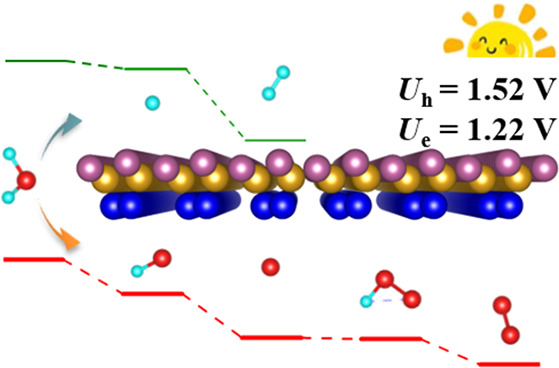
The design of materials meeting the rigorous requirements of photocatalytic water splitting is still a challenge. Anisotropic Janus 2D materials exhibit great potential due to outstandingly high photocatalytic efficiency. Unfortunately, these materials are scarce. By means of ab initio swarm-intelligence search calculations, we identify a SiP2 monolayer with Janus structure (i.e., out-of-plane asymmetry). The material turns out to be semiconducting with an indirect band gap of 2.39 eV enclosing the redox potentials of water. Notably, the oxygen and hydrogen evolution half reactions can happen simultaneously at the Si and P atoms, respectively, driven merely by the radiation-induced electrons and holes. The carrier mobility is found to be anisotropic and high, up to 10–4 cm2 V–1 s–1, facilitating fast transport of the photogenerated carriers. The SiP2 monolayer shows remarkably strong optical absorption in the visible-to-ultraviolet range of the solar spectrum, ensuring efficient utilization of the solar energy.
The modern economy and society demand huge amounts of energy, while the reserves of traditional fossil energy are limited, and the utilization of fossil energy pollutes the environment. Environmentally friendly, low-cost, and sustainable energy sources thus are in urgent demand. Photocatalytic decomposition of water into hydrogen (H2) and oxygen (O2) is the basis of one of the most promising energy sources, as it directly utilizes clean, renewable, and cost-free solar energy. While several breakthroughs have emerged since the pioneering work of Fujishima and Honda,1 the availability of nontoxic and highly efficient catalysts remains a key issue for large-scale applications.2,3
2D materials demonstrate unique advantages over traditional bulk materials for achieving highly efficient photocatalysis.4 In particular, large surface-to-volume ratios give rise to abundant active sites.5 Fast carrier transport and short distances maximize the utilization of the photogenerated carriers,6 and dependence of the electron properties on quantities such as the thickness, surface functionalization, and external strain makes it possible to enhance the utilization of the sunlight.7
A variety of 2D photocatalytic materials already have been studied experimentally and/or theoretically, such as g-C3N4,8 BN,9 phosphorene,10 transition-metal dichalcogenides,11 PdSeO3,12,13 and covalent organic frameworks,14 some demonstrating excellent efficiency. Still, photocatalysts for water splitting are rare. Thus, besides improving the performance of the known 2D materials,15 it is crucial to search for new candidates, not only to elevate the material properties but also to broaden the knowledge of 2D materials in general.16
Janus materials, a special kind of 2D materials, draw attention due to their out-of-plane asymmetry, inducing anisotropy, electric polarization, piezoelectricity, and magnetism suitable for novel electronic devices. The Janus structure also is able to improve the utilization of photogenerated carriers.17 The prototypical example is MoSSe (obtained by replacement of the S atoms on one side of 2D MoS2 with Se atoms), which exhibits large piezoelectricity.18 Several Janus materials, particularly M2X3 (M = Al, Ga, In; X = S, Se, Te)6 and B2P6,19 achieve an outstanding photocatalytic efficiency, even in excess of the conventional theoretical limit of 18%. They provide a route to realizing the oxygen evolution reaction (OER) and hydrogen evolution reaction (HER) simultaneously at different atomic species.20
Silicene, the 2D counterpart of widely used silicon, has a buckled honeycomb structure, realizes a mixture of sp2 and sp3 hybridization, and is nonmetallic, in sharp contract to graphene.21 Phosphorene combines a direct band gap with anisotropic mechanical, electronic (sp3 hybridization), and optical properties originating from its structural asymmetry.22,23 Three-coordination of Si or P atoms also facilitates the formation of a 2D structure. Indeed, several stable 2D SixPy materials have been reported with novel structures and extraordinary properties.24−26 While g-C3N4 shares with phosphorene the excellent catalytic performance, the weak absorption of sunlight limits applications.27 However, though C and Si as well as N and P belong to the same group of the periodic table, they are distinguished in terms of their electronegativity and will hybridize differently; i.e., a new 2D SixPy material still can realize strong optical absorption.
As currently ab initio structural prediction plays an important role in the discovery of new materials,28−30 we conduct in the present work a global search for the lowest-energy structure of 2D SixPy (x = 1–4 and y = 1–4). We identify stable semiconducting SiP2 and SiP3 monolayers. Interestingly, the SiP2 monolayer realizes an anisotropic Janus structure. It combines high carrier mobilities with strong optical absorption. The Si and P atoms give rise to active sites for the OER and HER, respectively, and it turns out that the photogenerated electrons and holes can trigger the two half reactions to occur simultaneously. This opens great potential of the SiP2 monolayer in photocatalytic water splitting.
We apply the crystal structure analysis by particle swarm optimization (CALYPSO) code;31,32 see details in the Supporting Information. Structure optimizations and electronic property calculations are performed in the framework of density functional theory, using the Vienna ab initio simulation package33,34 and projector augmented-wave35 pseudopotentials with Si 3s23p2 and P 3s23p3 valence states. The energy cutoff of the plane waves is set to 400 eV, the energy convergence to 10–6 eV, and the atomic force convergence to 10–3 eV Å–1. To create 2D models, a vacuum slab of ∼20 Å thickness is adopted. The Perdew–Burke–Ernzerhof36 functional is used for the structure optimizations, and to determine accurate band gaps and optical properties, we adopt the Heyd–Scuseria–Ernzerhof (HSE06)37 hybrid functional. Deformation potential theory is employed to predict the carrier mobilities;38 phonon dispersions are derived by the supercell approach of the Phonopy code,39 and molecular dynamics (MD) simulations are executed to evaluate the thermal stability. The MD simulations last 10 ps with a time step of 1 fs and are based on an NVT ensemble with Nosé–Hoover temperature control.40 20 O2 molecules are evenly distributed on the two sides of the SiP2 monolayer with the distance to the monolayer between 2 and 3 Å.
By extensive structural search, two hitherto unknown 2D materials with stoichiometries of SiP2 and SiP3 are identified (structural information in Tables S1 and S2). Other stoichiometries are incompatible with dynamical stability. SiP2 exhibits out-of-plane asymmetry (Janus structure; Figure 1a,b), consisting of a buckled honeycomb structure with alternating Si and P atoms, like silicene;41 and zigzag P chains, like 3D boron monophosphide42 and 2D AsP.43 Since the P atoms in the zigzag chains are connected to Si atoms, each Si/P atom in the honeycomb structure is three-coordinated with P/Si atoms, and each P atom in the zigzag chains connects to one Si and two P atoms, giving rise to an sp3 hybridization and satisfying the chemical octet rule for both the Si and P atoms. Notice that one of the P hybrid orbitals holds an electron lone pair (Figure 1c) and that the unique structural arrangement exposes the P atoms. The bonding is strongly covalent (Figure 1c,d), and the Si–P (2.28 Å) and P–P (2.27 Å) bond lengths are comparable to those in SiP (2.33 Å)44 and phosphorene (2.24 Å).45
Figure 1.
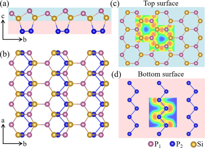
(a) Side and (b) top views of the SiP2 monolayer. Electron localization function in the (c) top and (d) bottom surfaces.
Being a prerequisite for application, we explore the dynamical, mechanical, thermal, and air stabilities of the SiP2 monolayer. The obtained phonon spectrum is indicative of dynamical stability (absence of imaginary frequencies throughout the Brillouin zone; Figure 2a). The highest frequency (529 cm–1) is comparable to results for Si3P (540 cm–1)26 and phosphorene (470 cm–1),46 demonstrating the formation of strong covalent bonds. MD simulations carried out for 10 ps at 300 and 1000 K show neither bond breaking nor significant structural distortions, verifying thermal stability (Figure S2). As P can easily react with the oxygen (O2) molecules in the air, like phosphorene,47 and considering that the P atoms of the SiP2 monolayer are strongly exposed to the environment, we employ MD simulations at 300 K to check the stability of a SiP2 monolayer with 20 O2 molecules in a 6 × 3 × 1 supercell. After 10 ps, the SiP2 monolayer remains intact, and the O2 molecules tend to separate from the monolayer without dissociating into oxygen atoms (Figure 2b). Similar results are obtained for CO2, H2, N2, and H2O molecules (Figure S3).
Figure 2.
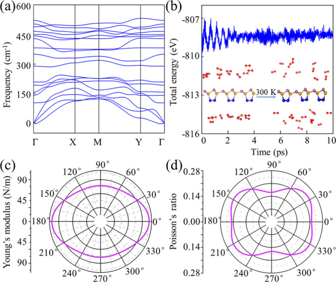
(a) Phonon spectrum of the SiP2 monolayer. Phonon densities of states can be found in Figure S1. (b) Total energy and snapshots of the SiP2 monolayer with 20 O2 molecules before and after a 10 ps MD simulation at 300 K. Polar diagrams of (c) E(θ) and (d) v(θ).
Based on the calculated linear elastic constants, the SiP2 monolayer is also mechanically stable (Supporting Information). Young’s modulus E(θ) characterizes a material’s flexibility/stiffness, and Poisson’s ratio v(θ) describes its mechanical response to an external load. We find that E(θ) varies from 77 to 105 N m–1 (Figure 2c), thus being smaller than that of graphene (342 N m–1)48 but comparable to that of phosphorene (24–102 N m–1).49 The in-plane flexibility of the SiP2 monolayer consequently is moderate. We further find that v(θ) varies from 0.16 to 0.24 (Figure 2d). The cohesive energy is useful to evaluate the prospects for experimental synthesis of a predicted 2D material. We find for the SiP2 monolayer a value of 3.98 eV atom–1. While this value is lower than those reported for graphene (7.91 eV atom–1)50 and 2D MoS2 (5.15 eV atom–1),51 it surpasses the cohesive energies of already existing silicene (3.91 eV atom–1),19 germanene (3.24 eV atom–1),19 and phosphorene (3.30 eV atom–1),52 indicating feasibility of experimental synthesis of the SiP2 monolayer.
We next explore the electronic properties of the SiP2 monolayer by studying the electron band structure and partial densities of states (PDOS). At the HSE06 level of theory, we find a semiconducting character with an indirect band gap of 2.39 eV (Figure 3a). Moreover, the conduction band minimum (CBM) is located at the M (0.5, 0.5, 0.0) point, and the valence band maximum (VBM) is located between the M and Y (0.0, 0.5, 0.0) points. Notably, the direct band gap of 2.51 eV at the Y point comes close to the indirect band gap. The PDOS shows strong Si–P hybridization (Figure 3b), pointing to covalent bonds, which is consistent with our above structural analysis. Both the VBM and CBM mainly originate from the Si 3p and P 3p orbitals. The charge densities at the VBM (Figure 3c) and CBM (Figure 3d) indicate that the π electron cloud is broken up by the electron lone pairs, as observed in PC6.53
Figure 3.
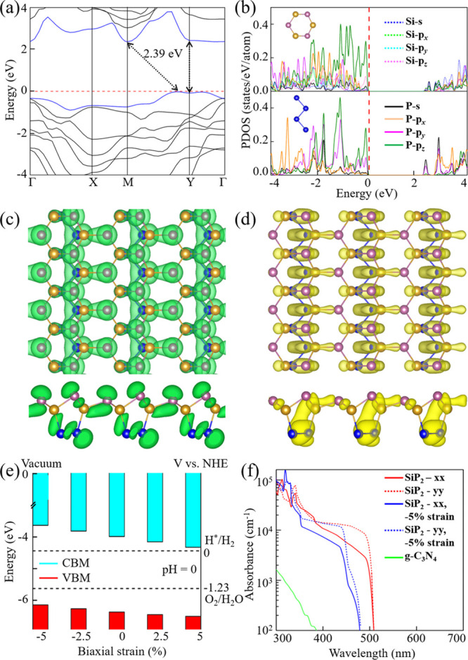
(a) Electronic band structure of the SiP2 monolayer. The horizontal dashed line is the VBM. (b) PDOS of the P and Si atoms in the Si3P3 honeycombs and the P atoms in the zigzag P chains. Top and side views of the charge densities at the (c) VBM and (d) CBM. (e) Energetic positions of the VBM and CBM under biaxial strain. The dashed lines mark the redox potentials of water at pH = 0. (f) Optical absorption coefficient of the SiP2 monolayer compared to g-C3N4.
While, in general, every semiconductor with a band gap between 1.23 and 3 eV is a potential photocatalyst for water splitting, the energetic positions of the VBM and CBM must be significantly lower and higher than the water oxidation potential (−5.67 eV) and hydrogen reduction potential (−4.44 eV) at pH = 0, respectively. The larger the energy differences, the better it is for the water splitting. The VBM (−6.37 eV) and CBM (−3.98 eV) of the SiP2 monolayer satisfy the thermodynamic requirements (Figure 3e). This remains valid under up to ±5% strain. While stretching supports the hydrogen reduction, compression supports the water oxidation.
An excellent photocatalyst must be able to harvest sunlight efficiently, particularly visible and ultraviolet light. To determine the optical absorption coefficient of the SiP2 monolayer in a reliable manner, the HSE06 level of theory is employed. Between 300 and 500 nm, we obtain values of up to 105 cm–1 (Figure 3f), which is much higher than that reported for g-C3N4.54 The obtained anisotropy of the optical adsorption is not very large. More interestingly, we find a red-shift of the spectrum under strain, supporting the utilization of visible light, while both the anisotropy and high optical absorption coefficient are maintained. Hence, the SiP2 monolayer can effectively harvest sunlight, facilitating utilization as a photocatalyst for water splitting.
Rapid transport of the photogenerated electrons and holes to the active sites is crucial for a highly efficient catalysis. High carrier mobility is also a prerequisite of many high-performance electronic devices.20 We aim to employ deformation potential theory to estimate the carrier mobility of the SiP2 monolayer. To verify that this approach is suitable, we predict the hole mobility of phosphorene as 2533 cm2 V–1 s–1, which is consistent with the reported value of 2200 cm2 V–1 s–1.55 The main parameters calculated for the SiP2 monolayer are given in Table 1. The high carrier mobilities outperform 2D MoS2 (200 cm2 V–1 s–1)56 and g-C3N4 (334 cm2 V–1 s–1),57 showing strong anisotropy with the lower electron and hole mobility along the a and b direction, respectively. This is mainly due to the direction-dependences (Table 1) of the deformation potential constant (larger/smaller in the a than the b direction for electrons/holes) and the effective mass (smaller in the a than the b direction for both electrons and holes) resulting from the structural anisotropy inherent to the SiP2 monolayer. Importantly, the SiP2 monolayer is able to ensure fast transport of the photogenerated electrons and holes to effectively participate in the redox reaction. While it is a challenge to achieve 2D materials that combine a large band gap with high carrier mobility and directional control,58−60 the SiP2 monolayer meets these requirements and thus is also a promising candidate for high-performance electronic devices.
Table 1. SiP2 Monolayer: Deformation Potential Constant (EDP), In-Plane Stiffness (C), Effective Mass (m*), Carrier Mobility (μ), and Relaxation Time (τ) along the a and b Directions at 300 K.
| carrier type | EDP (eV) | C (J m–2) | m* (m0) | μ (cm2 V–1 s–1) | τ (ps) |
|---|---|---|---|---|---|
| electron (a) | 12.51 | 101.28 | 0.13 | 212.36 | 0.02 |
| hole (a) | 0.31 | 101.28 | 0.78 | 3.20 × 10⁴ | 15.60 |
| electron (b) | 0.23 | 76.99 | 1.90 | 3.27 × 10⁴ | 38.80 |
| hole (b) | 0.58 | 76.99 | 1.03 | 5.27 × 10³ | 3.39 |
To study whether the photogenerated electrons and holes can provide enough driving force to trigger the OER and HER, we focus on neutral conditions (pH = 7). The energetic positions of the VBM and CBM still enclose the redox potentials of water. The calculated potentials of the photogenerated electrons and holes are Ue = 0.87 V and Uh = 1.52 V, respectively, and the obtained reaction pathways, structures, and Gibbs free energies are illustrated in Figure 4a,b. For the OER and HER, absorption is favorable at the Si and P atoms, respectively, due to the higher electronegativity of P as compared to Si. Coexistence of active sites for both reactions boosts the photocatalytic efficiency by avoiding recombination of photogenerated carriers.20
Figure 4.
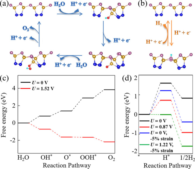
Proposed photocatalytic pathways of the (a) oxygen and (b) hydrogen evolution half reactions on the SiP2 monolayer for the (energetically favorable) intermediates OH*, O*, OOH*, and H*. The red and green balls are O and H atoms, respectively. Gibbs free energy diagrams of the (c) OER and (d) HER on the SiP2 monolayer for different conditions.
In a dark environment (Uh = 0 V, black line in Figure 4c), the Gibbs free energy increases in each of the four steps of the OER, indicating that the reaction does not proceed spontaneously. ΔGOOH* = 1.50 V is the largest increase of the Gibbs free energy and thus the limiting potential, which consequently is much smaller than in the case of g-C3N4 (2.28 V).61 In a light environment (Uh = 1.52 V, red line in Figure 4c), the photogenerated holes provide a driving force, and the Gibbs free energy thus decreases in each step; i.e., the molecules can be oxidized into O2 in neutral conditions. Like the OER, the HER, which comprises two steps, does not proceed spontaneously in a dark environment (Figure 4d), but it can occur in a light environment under 5% compression. Compression of the SiP2 monolayer therefore enhances not only the optical absorption (Figure 3e) but also the driving force of the photogenerated electrons (Figure 3f), enabling efficient photocatalysis.
We finally turn to the discovered SiP3 monolayer, which shows a monoclinic structure with space group C2/m and four formula units per unit cell (Figure 5a–c). The Si and P atoms show sp3 hybridization and covalent bonds, satisfying the chemical octet rule. The cohesive energy turns out to be 3.80 eV atom–1. It is thus slightly lower than that found for the SiP2 monolayer, but exceeds the literature values reported for the SiP (3.64 eV atom–1) and Si3P (3.78 eV atom–1) monolayers.26
Figure 5.
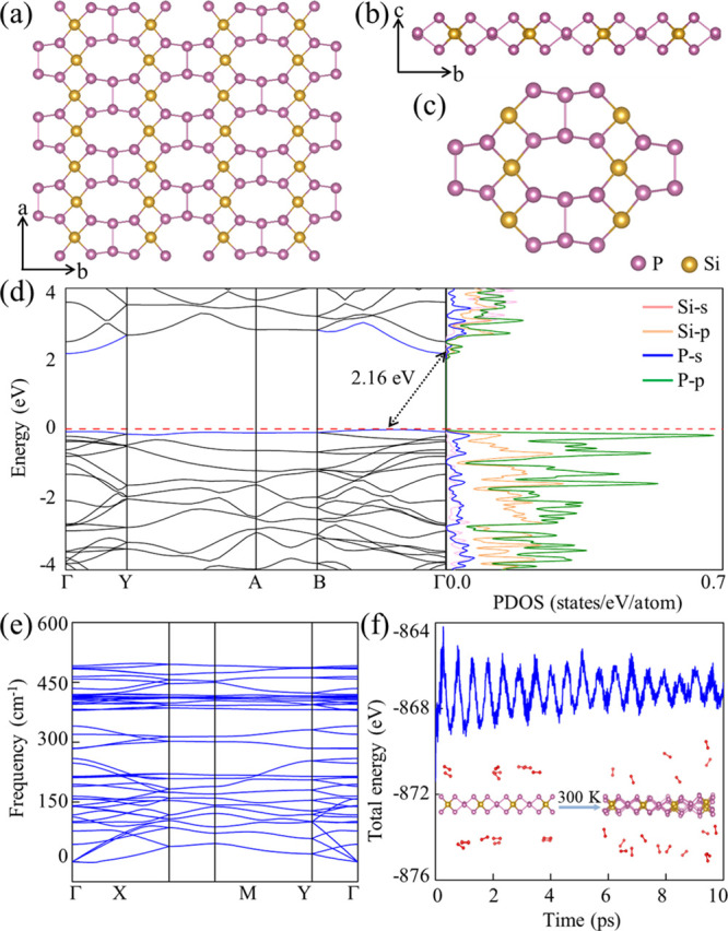
(a) Top and (b) side views of the SiP3 monolayer and (c) basic building block (Si6P20). (d) Electronic band structure and PDOS. The horizontal dashed line is the VBM. (e) Phonon spectrum. Phonon densities of states can be found in Figure S1. (f) Total energy and snapshots of the SiP3 monolayer with 20 O2 molecules before and after a 10 ps MD simulation at 300 K.
The SiP3 monolayer is an indirect band gap (2.16 eV at the HSE06 level of theory; Figure 5d) semiconductor and dynamically (Figure 5e) and thermally (Figure 5f and Figure S2) stable. The electron and hole mobilities are anisotropic, with a particularly large electron mobility along the a direction (Table 2). Generally, 2D materials can enhance the performance of field effect transistors due to confinement of the charge carriers in atomically thin channels.62,63 Considering its moderate band gap and high electron mobility, outperforming 2D MoS2,56 the SiP3 monolayer has great potential in this field.
Table 2. SiP3 Monolayer: Deformation Potential Constant (EDP), In-Plane Stiffness (C), Effective Mass (m*), Carrier Mobility (μ), and Relaxation Time (τ) along the a and b Directions at 300 K.
| carrier type | EDP (eV) | C (J m–2) | m* (m0) | μ (cm2 V–1 s–1) | τ (ps) |
|---|---|---|---|---|---|
| electron (a) | 1.16 | 35.95 | 0.47 | 2.33 × 10³ | 0.68 |
| hole (a) | 1.68 | 35.95 | 5.71 | 12.39 | 0.04 |
| electron (b) | 3.01 | 73.71 | 0.58 | 575.38 | 0.21 |
| hole (b) | 2.63 | 73.71 | 2.58 | 22.94 | 0.04 |
The structural motifs of the SiP2 monolayer (zigzag P chains) and SiP3 monolayer (Si6P20 units consisting of edge-sharing Si2P2 quadrangles and SiP4 pentagons) complement the four motifs (Figure S4) reported in the literature for 2D SiP,25,26,44 2D SiP2,24 and 2D Si3P.26 In the case of 2D SiP, buckled hexagonal Si3P3 rings, consisting of alternating Si and P atoms,26,44 and interconnected chairlike Si3P3 and Si3P2 rings, in which the Si atoms are four-coordinated,25 have been reported. In the case of 2D SiP2, a chairlike Si3P3 ring and two Si2P3 rings share edges, leading to distorted P chains.24 The basic structural unit of 2D Si3P is Si6P6, where each Si atom of a central hexagonal ring bonds to a P atom.26 Great variability in the structural motifs therefore is found to be characteristic of 2D SixPy.
In conclusion, we discover two 2D materials, the SiP2 and SiP3 monolayers, through a combination of evolutionary search and ab initio calculations. For the SiP2 monolayer we obtain a Janus structure with high thermal and dynamical stabilities resulting from strong Si–P and P–P covalent bonds that satisfy the chemical octet rule. The SiP2 monolayer shows remarkably high carrier mobilities of the order of 10–4 cm2 V–1 s–1 with preferential electron transport along the b direction and hole transport along the a direction. Also, the optical absorption coefficient is high. Interestingly, the Si and P atoms give rise to active sites for the OER and HER, respectively, and we find that the material is capable of splitting water into O2 and H2 under sunlight. Overall, we demonstrate that the SiP2 monolayer is an excellent candidate for photocatalytic water splitting.
Acknowledgments
The authors acknowledge funding from the Natural Science Foundation of China under 21873017 and 21573037, the Postdoctoral Science Foundation of China under grant 2013M541283, and the Natural Science Foundation of Jilin Province (20190201231JC). The research reported in this publication was supported by funding from King Abdullah University of Science and Technology (KAUST). The work was carried out at the National Supercomputer Center in Tianjin, and the calculations were performed on TianHe-1 (A).
Supporting Information Available
The Supporting Information is available free of charge at https://pubs.acs.org/doi/10.1021/acs.jpclett.0c03841.
Description of the computational methods and detailed structural information on the SiP2 and SiP3 monolayers (PDF)
Author Contributions
∥ T.Y. and C.W. contributed equally.
The authors declare no competing financial interest.
Supplementary Material
References
- Fujishima A.; Honda K. Electrochemical Photolysis of Water at a Semiconductor Electrode. Nature 1972, 238, 37–38. 10.1038/238037a0. [DOI] [PubMed] [Google Scholar]
- Wang Z.; Li C.; Domen K. Recent Developments in Heterogeneous Photocatalysts for Solar-Driven Overall Water Splitting. Chem. Soc. Rev. 2019, 48, 2109–2125. 10.1039/C8CS00542G. [DOI] [PubMed] [Google Scholar]
- Lin L.; Yu Z.; Wang X. Crystalline Carbon Nitride Semiconductors for Photocatalytic Water Splitting. Angew. Chem., Int. Ed. 2019, 58, 6164–6175. 10.1002/anie.201809897. [DOI] [PubMed] [Google Scholar]
- Faraji M.; Yousefi M.; Yousefzadeh S.; Zirak M.; Naseri N.; Jeon T. H.; Choi W.; Moshfegh A. Z. Two-Dimensional Materials in Semiconductor Photoelectrocatalytic Systems for Water Splitting. Energy Environ. Sci. 2019, 12, 59–95. 10.1039/C8EE00886H. [DOI] [Google Scholar]
- Wang L.; Zhang Y.; Chen L.; Xu H.; Xiong Y. 2D Polymers As Emerging Materials for Photocatalytic Overall Water Splitting. Adv. Mater. 2018, 30, 1801955. 10.1002/adma.201801955. [DOI] [PubMed] [Google Scholar]
- Fu C. F.; Sun J.; Luo Q.; Li X.; Hu W.; Yang J. Intrinsic Electric Fields in Two-Dimensional Materials Boost the Solar-To-Hydrogen Efficiency for Photocatalytic Water Splitting. Nano Lett. 2018, 18, 6312–6317. 10.1021/acs.nanolett.8b02561. [DOI] [PubMed] [Google Scholar]
- Gu D.; Tao X.; Chen H.; Zhu W.; Ouyang Y.; Peng Q. Enhanced Photocatalytic Activity for Water Splitting of Blue-Phase GeS and GeSe Monolayers: Via Biaxial Straining. Nanoscale 2019, 11, 2335–2342. 10.1039/C8NR08908F. [DOI] [PubMed] [Google Scholar]
- Zheng Y.; Lin L.; Ye X.; Guo F.; Wang X. Helical Graphitic Carbon Nitrides with Photocatalytic and Optical Activities. Angew. Chem. 2014, 126, 12120–12124. 10.1002/ange.201407319. [DOI] [PubMed] [Google Scholar]
- Huang C.; Chen C.; Zhang M.; Lin L.; Ye X.; Lin S.; Antonietti M.; Wang X. Carbon-Doped BN Nanosheets for Metal-Free Photoredox Catalysis. Nat. Commun. 2015, 6, 7698. 10.1038/ncomms8698. [DOI] [PMC free article] [PubMed] [Google Scholar]
- Hu W.; Lin L.; Zhang R.; Yang C.; Yang J. Highly Efficient Photocatalytic Water Splitting Over Edge-Modified Phosphorene Nanoribbons. J. Am. Chem. Soc. 2017, 139, 15429–15436. 10.1021/jacs.7b08474. [DOI] [PubMed] [Google Scholar]
- Fang Q.; Zhao X.; Huang Y.; Xu K.; Min T.; Chu P. K.; Ma F. Interfacial Electronic States and Self-Formed p-n Junctions in Hydrogenated MoS2/SiC Heterostructure. J. Mater. Chem. C 2018, 6, 4523–4530. 10.1039/C8TC00742J. [DOI] [Google Scholar]
- Qiao M.; Liu J.; Wang Y.; Li Y.; Chen Z. PdSeO3 Monolayer: Promising Inorganic 2D Photocatalyst for Direct Overall Water Splitting Without Using Sacrificial Reagents and Cocatalysts. J. Am. Chem. Soc. 2018, 140, 12256–12262. 10.1021/jacs.8b07855. [DOI] [PubMed] [Google Scholar]
- Zhang X.; Liu J.; Zhang E.; Pan R.; Li Y.; Wan X.; Wang H.; Zhang J. Atomically Thin PdSeO3 Nanosheets: A Promising 2D Photocatalyst Produced by Quaternary Ammonium Intercalation and Exfoliation. Chem. Commun. 2020, 56, 5504–5507. 10.1039/D0CC01642J. [DOI] [PubMed] [Google Scholar]
- Wan Y.; Wang L.; Xu H.; Wu X.; Yang J. A Simple Molecular Design Strategy for Two-Dimensional Covalent Organic Framework Capable of Visible-Light-Driven Water Splitting. J. Am. Chem. Soc. 2020, 142, 4508–4516. 10.1021/jacs.0c00564. [DOI] [PubMed] [Google Scholar]
- Ju L.; Shang J.; Tang X.; Kou L. Tunable Photocatalytic Water Splitting by the Ferroelectric Switch in a 2D AgBiP2Se6 Monolayer. J. Am. Chem. Soc. 2020, 142, 1492–1500. 10.1021/jacs.9b11614. [DOI] [PubMed] [Google Scholar]
- Zhang X.; Zhang Z.; Wu D.; Zhang X.; Zhao X.; Zhou Z. Computational Screening of 2D Materials and Rational Design of Heterojunctions for Water Splitting Photocatalysts. Small Methods 2018, 2, 1700359. 10.1002/smtd.201700359. [DOI] [Google Scholar]
- Dong L.; Lou J.; Shenoy V. B. Large In-Plane and Vertical Piezoelectricity in Janus Transition Metal Dichalchogenides. ACS Nano 2017, 11, 8242–8248. 10.1021/acsnano.7b03313. [DOI] [PubMed] [Google Scholar]
- Lu A. Y.; Zhu H.; Xiao J.; Chuu C. P.; Han Y.; Chiu M. H.; Cheng C. C.; Yang C. W.; Wei K. H.; Yang Y.; et al. Janus Monolayers of Transition Metal Dichalcogenides. Nat. Nanotechnol. 2017, 12, 744–749. 10.1038/nnano.2017.100. [DOI] [PubMed] [Google Scholar]
- Sun M.; Schwingenschlögl U. B2P6: A Two-Dimensional Anisotropic Janus Material with Potential in Photocatalytic Water Splitting and Metal-Ion Batteries. Chem. Mater. 2020, 32, 4795–4800. 10.1021/acs.chemmater.0c01536. [DOI] [Google Scholar]
- Ju L.; Bie M.; Tang X.; Shang J.; Kou L. Janus WSSe Monolayer: An Excellent Photocatalyst for Overall Water Splitting. ACS Appl. Mater. Interfaces 2020, 12, 29335–29343. 10.1021/acsami.0c06149. [DOI] [PubMed] [Google Scholar]
- Tao L.; Cinquanta E.; Chiappe D.; Grazianetti C.; Fanciulli M.; Dubey M.; Molle A.; Akinwande D. Silicene Field-Effect Transistors Operating at Room Temperature. Nat. Nanotechnol. 2015, 10, 227–231. 10.1038/nnano.2014.325. [DOI] [PubMed] [Google Scholar]
- Li L.; Yu Y.; Ye G. J.; Ge Q.; Ou X.; Wu H.; Feng D.; Chen X. H.; Zhang Y. Black Phosphorus Field-Effect Transistors. Nat. Nanotechnol. 2014, 9, 372–377. 10.1038/nnano.2014.35. [DOI] [PubMed] [Google Scholar]
- Qiao J.; Kong X.; Hu Z. X.; Yang F.; Ji W. High-Mobility Transport Anisotropy and Linear Dichroism in Few-Layer Black Phosphorus. Nat. Commun. 2014, 5, 4475. 10.1038/ncomms5475. [DOI] [PMC free article] [PubMed] [Google Scholar]
- Matta S. K.; Zhang C.; Jiao Y.; O’Mullane A.; Du A. Versatile Two-Dimensional Silicon Diphosphide (SiP2) for Photocatalytic Water Splitting. Nanoscale 2018, 10, 6369–6374. 10.1039/C7NR07994J. [DOI] [PubMed] [Google Scholar]
- Zhang S.; Guo S.; Huang Y.; Zhu Z.; Cai B.; Xie M.; Zhou W.; Zeng H. Two-Dimensional SiP: An Unexplored Direct Band-Gap Semiconductor. 2D Mater. 2017, 4, 015030. 10.1088/2053-1583/4/1/015030. [DOI] [Google Scholar]
- Ding Y.; Wang Y. Density Functional Theory Study of the Silicene-like SiX and XSi3 (X = B, C, N, Al, P) Honeycomb Lattices: The Various Buckled Structures and Versatile Electronic Properties. J. Phys. Chem. C 2013, 117, 18266–18278. 10.1021/jp407666m. [DOI] [Google Scholar]
- Che W.; Cheng W.; Yao T.; Tang F.; Liu W.; Su H.; Huang Y.; Liu Q.; Liu J.; Hu F.; et al. Fast Photoelectron Transfer in (Cring)-C3N4 Plane Heterostructural Nanosheets for Overall Water Splitting. J. Am. Chem. Soc. 2017, 139, 3021–3026. 10.1021/jacs.6b11878. [DOI] [PubMed] [Google Scholar]
- Jain A.; Shin Y.; Persson K. A. Computational Predictions of Energy Materials Using Density Functional Theory. Nat. Rev. Mater. 2016, 1, 15004. 10.1038/natrevmats.2015.4. [DOI] [Google Scholar]
- Zhang L.; Wang Y.; Lv J.; Ma Y. Materials Discovery at High Pressures. Nat. Rev. Mater. 2017, 2, 17005. 10.1038/natrevmats.2017.5. [DOI] [Google Scholar]
- Oganov A. R.; Pickard C. J.; Zhu Q.; Needs R. J. Structure Prediction Drives Materials Discovery. Nat. Rev. Mater. 2019, 4, 331–348. 10.1038/s41578-019-0101-8. [DOI] [Google Scholar]
- Wang Y.; Lv J.; Zhu L.; Ma Y. CALYPSO: A Method for Crystal Structure Prediction. Comput. Phys. Commun. 2012, 183, 2063–2070. 10.1016/j.cpc.2012.05.008. [DOI] [Google Scholar]
- Wang Y.; Lv J.; Zhu L.; Ma Y. Crystal Structure Prediction Via Particle-Swarm Optimization. Phys. Rev. B: Condens. Matter Mater. Phys. 2010, 82, 94116. 10.1103/PhysRevB.82.094116. [DOI] [Google Scholar]
- Kohn W.; Sham L. J. Self-Consistent Equations Including Exchange and Correlation Effects. Phys. Rev. 1965, 140, A1133–A1138. 10.1103/PhysRev.140.A1133. [DOI] [Google Scholar]
- Kresse G.; Furthmüller J. Efficient Iterative Schemes for Ab Initio Total-Energy Calculations Using a Plane-Wave Basis Set. Phys. Rev. B: Condens. Matter Mater. Phys. 1996, 54, 11169–11186. 10.1103/PhysRevB.54.11169. [DOI] [PubMed] [Google Scholar]
- Blöchl P. E. Projector Augmented-Wave Method. Phys. Rev. B: Condens. Matter Mater. Phys. 1994, 50, 17953–17979. 10.1103/PhysRevB.50.17953. [DOI] [PubMed] [Google Scholar]
- Paier J.; Hirschl R.; Marsman M.; Kresse G. The Perdew-Burke-Ernzerhof Exchange-Correlation Functional Applied to the G2–1 Test Set Using a Plane-Wave Basis Set. J. Chem. Phys. 2005, 122, 234102. 10.1063/1.1926272. [DOI] [PubMed] [Google Scholar]
- Heyd J.; Scuseria G. E.; Ernzerhof M. Hybrid Functionals Based on a Screened Coulomb Potential. J. Chem. Phys. 2003, 118, 8207–8215. 10.1063/1.1564060. [DOI] [Google Scholar]
- Bardeen J.; Shockley W. Deformation Potentials and Mobilities in Non-Polar Crystals. Phys. Rev. 1950, 80, 72–80. 10.1103/PhysRev.80.72. [DOI] [Google Scholar]
- Togo A.; Oba F.; Tanaka I. First-Principles Calculations of the Ferroelastic Transition Between Rutile-Type and CaCl2-Type SiO2 at High Pressures. Phys. Rev. B: Condens. Matter Mater. Phys. 2008, 78, 134106. 10.1103/PhysRevB.78.134106. [DOI] [Google Scholar]
- Martyna G. J.; Klein M. L.; Tuckerman M. Nose-Hoover Chains: The Canonical Ensemble Via Continuous Dynamics. J. Chem. Phys. 1992, 97, 2635–2643. 10.1063/1.463940. [DOI] [Google Scholar]
- Yan J.-A.; Stein R.; Schaefer D. M.; Wang X.-Q.; Chou M. Y. Electron-Phonon Coupling in Two-Dimensional Silicene and Germanene. Phys. Rev. B: Condens. Matter Mater. Phys. 2013, 88, 121403. 10.1103/PhysRevB.88.121403. [DOI] [Google Scholar]
- Zhang X.; Qin J.; Liu H.; Zhang S.; Ma M.; Luo W.; Liu R.; Ahuja R. Pressure-Induced Zigzag Phosphorus Chain and Superconductivity in Boron Monophosphide. Sci. Rep. 2015, 5, 8761. 10.1038/srep08761. [DOI] [PMC free article] [PubMed] [Google Scholar]
- Cai X.; Chen Y.; Sun B.; Chen J.; Wang H.; Ni Y.; Tao L.; Wang H.; Zhu S.; Li X.; et al. Two-Dimensional Blue-AsP Monolayers with Tunable Direct Band Gap and Ultrahigh Carrier Mobility Show Promising High-Performance Photovoltaic Properties. Nanoscale 2019, 11, 8260–8269. 10.1039/C9NR01261C. [DOI] [PubMed] [Google Scholar]
- Ma Z.; Zhuang J.; Zhang X.; Zhou Z. SiP Monolayers: New 2D Structures of Group IV-V Compounds for Visible-Light Photohydrolytic Catalysts. Front. Phys. 2018, 13, 138104. 10.1007/s11467-018-0760-8. [DOI] [Google Scholar]
- Li X.-B.; Guo P.; Cao T.-F.; Liu H.; Lau W.-M.; Liu L.-M. Structures, Stabilities and Electronic Properties of Defects in Monolayer Black Phosphorus. Sci. Rep. 2015, 5, 10848. 10.1038/srep10848. [DOI] [PMC free article] [PubMed] [Google Scholar]
- Cai Y.; Ke Q.; Zhang G.; Feng Y. P.; Shenoy V. B.; Zhang Y. W. Giant Phononic Anisotropy and Unusual Anharmonicity of Phosphorene: Interlayer Coupling and Strain Engineering. Adv. Funct. Mater. 2015, 25, 2230–2236. 10.1002/adfm.201404294. [DOI] [Google Scholar]
- Wood J. D.; Wells S. A.; Jariwala D.; Chen K. S.; Cho E.; Sangwan V. K.; Liu X.; Lauhon L. J.; Marks T. J.; Hersam M. C. Effective Passivation of Exfoliated Black Phosphorus Transistors against Ambient Degradation. Nano Lett. 2014, 14, 6964–6970. 10.1021/nl5032293. [DOI] [PubMed] [Google Scholar]
- Xiang P.; Sharma S.; Wang Z. M.; Wu J.; Schwingenschlögl U. Flexible C6BN Monolayers As Promising Anode Materials for High-Performance K-Ion Batteries. ACS Appl. Mater. Interfaces 2020, 12, 30731–30739. 10.1021/acsami.0c09451. [DOI] [PMC free article] [PubMed] [Google Scholar]
- Xu X.; Ma Y.; Zhang T.; Lei C.; Huang B.; Dai Y. Prediction of Two-Dimensional Antiferromagnetic Ferroelasticity in an AgF2 Monolayer. Nanoscale Horiz. 2020, 5, 1386–1393. 10.1039/D0NH00362J. [DOI] [PubMed] [Google Scholar]
- Shin H.; Kang S.; Koo J.; Lee H.; Kim J.; Kwon Y. Cohesion Energetics of Carbon Allotropes: Quantum Monte Carlo Study. J. Chem. Phys. 2014, 140, 114702. 10.1063/1.4867544. [DOI] [PubMed] [Google Scholar]
- Ataca C.; Topsakal M.; Aktürk E.; Ciraci S. A Comparative Study of Lattice Dynamics of Three- and Two-Dimensional MoS2. J. Phys. Chem. C 2011, 115, 16354–16361. 10.1021/jp205116x. [DOI] [Google Scholar]
- Guan J.; Zhu Z.; Tománek D. Phase Coexistence and Metal-Insulator Transition in Few-Layer Phosphorene: A Computational Study. Phys. Rev. Lett. 2014, 113, 046804. 10.1103/PhysRevLett.113.046804. [DOI] [PubMed] [Google Scholar]
- Yu T.; Zhao Z.; Sun Y.; Bergara A.; Lin J.; Zhang S.; Xu H.; Zhang L.; Yang G.; Liu Y. Two-Dimensional PC6 with Direct Band Gap and Anisotropic Carrier Mobility. J. Am. Chem. Soc. 2019, 141, 1599–1605. 10.1021/jacs.8b11350. [DOI] [PubMed] [Google Scholar]
- Mamba G.; Mishra A. K. Graphitic Carbon Nitride (g-C3N4) Nanocomposites: A New and Exciting Generation of Visible Light Driven Photocatalysts for Environmental Pollution Remediation. Appl. Catal., B 2016, 198, 347–377. 10.1016/j.apcatb.2016.05.052. [DOI] [Google Scholar]
- Fei R.; Yang L. Strain-Engineering the Anisotropic Electrical Conductance of Few-Layer Black Phosphorus. Nano Lett. 2014, 14, 2884–2889. 10.1021/nl500935z. [DOI] [PubMed] [Google Scholar]
- Cai Y.; Zhang G.; Zhang Y. W. Polarity-Reversed Robust Carrier Mobility in Monolayer MoS2 Nanoribbons. J. Am. Chem. Soc. 2014, 136, 6269–6275. 10.1021/ja4109787. [DOI] [PubMed] [Google Scholar]
- He Y.; Zhang M.; Shi J.-J.; Zhu Y.-H.; Cen Y.-L.; Wu M.; Guo W.-H.; Ding Y.-M. Two-Dimensional g-C3N4/InSe Heterostructure As a Novel Visible-Light Photocatalyst for Overall Water Splitting: A First-Principles Study. J. Phys. D: Appl. Phys. 2019, 52, 15304. 10.1088/1361-6463/aae67d. [DOI] [Google Scholar]
- Guo S.; Zhu Z.; Hu X.; Zhou W.; Song X.; Zhang S.; Zhang K.; Zeng H. Ultrathin Tellurium Dioxide: Emerging Direct Bandgap Semiconductor with High-Mobility Transport Anisotropy. Nanoscale 2018, 10, 8397–8403. 10.1039/C8NR01028E. [DOI] [PubMed] [Google Scholar]
- Fiori G.; Bonaccorso F.; Iannaccone G.; Palacios T.; Neumaier D.; Seabaugh A.; Banerjee S. K.; Colombo L. Electronics Based on Two-Dimensional Materials. Nat. Nanotechnol. 2014, 9, 768–779. 10.1038/nnano.2014.207. [DOI] [PubMed] [Google Scholar]
- Simon J.; Protasenko V.; Lian C.; Xing H.; Jena D. Polarization-Induced Hole Doping in Wide-Band-Gap Uniaxial Semiconductor Heterostructures. Science 2010, 327, 60–64. 10.1126/science.1183226. [DOI] [PubMed] [Google Scholar]
- Zhang Y.; Antonietti M. Photocurrent Generation by Polymeric Carbon Nitride Solids: An Initial Step Towards a Novel Photovoltaic System. Chem. - Asian J. 2010, 5, 1307–1311. 10.1002/asia.200900685. [DOI] [PubMed] [Google Scholar]
- Liu E.; Fu Y.; Wang Y.; Feng Y.; Liu H.; Wan X.; Zhou W.; Wang B.; Shao L.; Ho C. H.; et al. Integrated Digital Inverters Based on Two-Dimensional Anisotropic ReS2 Field-Effect Transistors. Nat. Commun. 2015, 6, 6991. 10.1038/ncomms7991. [DOI] [PMC free article] [PubMed] [Google Scholar]
- Desai S. B.; Madhvapathy S. R.; Sachid A. B.; Llinas J. P.; Wang Q.; Ahn G. H.; Pitner G.; Kim M. J.; Bokor J.; Hu C.; et al. MoS2 Transistors with 1-Nanometer Gate Lengths. Science 2016, 354, 99–102. 10.1126/science.aah4698. [DOI] [PubMed] [Google Scholar]
Associated Data
This section collects any data citations, data availability statements, or supplementary materials included in this article.


