

Low-dimensional Te-based photodetectors exhibit blackbody response and achieve record-set performance metrics.
Abstract
Blackbody-sensitive room-temperature infrared detection is a notable development direction for future low-dimensional infrared photodetectors. However, because of the limitations of responsivity and spectral response range for low-dimensional narrow bandgap semiconductors, few low-dimensional infrared photodetectors exhibit blackbody sensitivity. Here, highly crystalline tellurium (Te) nanowires and two-dimensional nanosheets were synthesized by using chemical vapor deposition. The low-dimensional Te shows high hole mobility and broadband detection. The blackbody-sensitive infrared detection of Te devices was demonstrated. A high responsivity of 6650 A W−1 (at 1550-nm laser) and the blackbody responsivity of 5.19 A W−1 were achieved. High-resolution imaging based on Te photodetectors was successfully obtained. All the results suggest that the chemical vapor deposition–grown low-dimensional Te is one of the competitive candidates for sensitive focal-plane-array infrared photodetectors at room temperature.
INTRODUCTION
Blackbody response has been widely applied as one of the standard characterizations for infrared focal plane array detectors, which is an important parameter reflecting the sensitivity of infrared photodetectors and determines the corresponding practical applications (1). Up to now, most of the available and high-performance infrared photodetectors with blackbody response are based on traditional III-V and II-VI materials such as InGaAs, InSb, and HgCdTe (2–4). However, high growth costs of molecule beam epitaxy, metal-organic chemical vapor deposition, and other epitaxial growth methods, as well as the strict cooling requirements, severely limit the wider application and promotion of these traditional infrared detectors. With the rise and gradual development of low-dimensional materials, narrow bandgap low-dimensional materials have exhibited extraordinary potential for the next-generation infrared photodetectors operating at room temperature (5–8). The unique out-of-plane van der Waals force of low-dimensional layered materials makes them free from the surface dangling bonds compared to traditional materials, which reduces the dark current of the devices from surface recombination (9). On the other hand, because of the quantum confinement, the strong light-matter interaction of low-dimensional materials enables them to exhibit excellent photodetection (10). Currently, the ultrahigh responsivity and detectivity of low-dimensional infrared detectors have been obtained under infrared laser illumination (11–14). However, in the practical applications of infrared photodetectors, blackbody source radiation is more similar to the actual irradiation of the detected object rather than the laser source. Blackbody sensitivity means that the low-dimensional system detectors could take an important step toward commercial applications. Up to now, only a few infrared photodetectors based on quantum dots, carbon tubes, and black phosphorus (BP) are reported to have a response to the blackbody radiation (9, 15–18).
Black phosphorous infrared detectors have exhibited excellent performance, but the difficult large-area growth and poor stability impede the practical applications (16). The strong exciton effect in the carbon tubes and the low mobility of the disordered carbon tube films strongly limit the performance of the carbon tube infrared detectors (19). The poor crystallinity of the quantum dot film and its low mobility limit the response time and bandwidth of its infrared detector (17).
Here, we report numerous and high-quality low-dimensional Te synthesized by low-cost chemical vapor deposition (CVD), including nanosheets and nanowires. The morphology evolution and growth kinetics of low-dimensional Te during the growth process are elaborated by density function theory (DFT). Photodetectors based on Te nanosheets and nanowires show an excellent blackbody and polarization response. Our work provides a previously unknown avenue for high-performance blackbody-sensitive room-temperature low-dimensional materials infrared photodetectors with an efficient and large-scale fabrication.
RESULTS AND DISCUSSION
Material characterizations
Figure 1 (A and B) shows the scanning electron microscopy (SEM) images of CVD-synthesized tellurium nanosheets and nanowires on the Si substrate, respectively. The insets in Fig. 1 (A and B) are high-magnification SEM images of Te nanosheets and nanowires, respectively. It is found that Te nanosheets exhibit regular shapes including rectangle, pentagon, and hexagon. The length and width of Te nanosheets exceed and reach up to 50 and 20 μm, respectively. The diameter of Te nanowires is approximately 200 nm. Meanwhile, the transmission electron microscopy (TEM) characterization of Te nanosheets and nanowires are displayed in Fig. 1 (C and F). The size, smooth, and neat surface topography of the samples are observed, present in the insets of Fig. 1 (B and E). Figure 1 (B and E) shows the high-resolution TEM (HRTEM) images of Te nanosheet and nanowire, respectively. The corresponding selected-area electron diffraction (SAED) images are exhibited in Fig. 1 (D and F), respectively. The HRTEM and SAED demonstrate that both nanosheet and nanowire have high crystallinity. The interplanar spacing distances of both Te nanosheet and nanowire in HRTEM image are approximately 0.59 nm, which is consistent with the spacing distance of (001) lattice planes of hexagonal Te in previous work (20). The corresponding SAED images show the distinctive and sharp diffraction of the Te nanosheets and nanowires, which further confirm the excellent single-crystalline of CVD-grown Te with the unique hexagonal structure and corresponding crystal planar spacing distance. The crystal phase of tellurium is confirmed by x-ray diffraction (XRD) in Fig. 1G. The characteristic and sharp peaks of as-grown Te indicate the good crystallinity of Te nanosheets and nanowires with the growth direction along the <100> axis. Figure 1H shows the schematic diagram of the Te crystal structure, where the covalently bonded atoms are arranged by uniaxial spiral connection, and these chains are connected into a hexagonal structure by Van der Waals force. This unique in-plane asymmetry chiral-chain structure also means that this material should be anisotropic. The atomic force microscopy (AFM) images and Raman spectrum without impurity peaks of Te nanosheets are shown in fig. S1, further exhibiting a good crystallinity of Te nanosheets. Moreover, angle-resolved polarized Raman spectroscopy was used to further study the anisotropy properties of Te nanosheets, as shown in fig. S1C. The absorption spectrum of Te nanosheets in Fig. 1I indicates that the absorption cutoff wavelength was approximately 0.35 eV (corresponding to 3.5-μm wavelength). Overall, the narrow optical bandgap, significant anisotropy, and excellent crystallinity ensure that infrared photodetector devices based on low-dimensional Te could exhibit excellent optoelectronic performance.
Fig. 1. Morphological and material characterizations of low-dimensional Te.
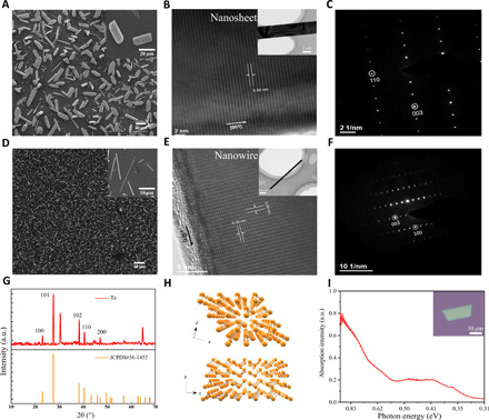
(A and D) SEM images of Te nanosheets and nanowires. Insets are corresponding high-magnification SEM images. (B and E) HRTEM of Te nanosheets and nanowires. Insets are corresponding low-magnification TEM images. (C and F) Corresponding SAED images of Te nanosheets and nanowires. Interplanar spacings of 0.59, 022, and 0.38 nm are the (001), (101), and (100) lattice planes, respectively. (G) XRD of CVD-grown Te, which is in agreement with the standard powder diffraction file (PDF) card (JCPDS#36-1452). The unmarked peak around 30° is the main peak of TeO3 corresponding to the PDF card (JCPDS#22-0911). (H) Schematic illustration of Te crystal structure. (I) Absorption spectrum of Te nanosheet. Insets are the corresponding optical microscopy image of Te nanosheet. a.u., arbitrary units.
Growth mechanism of low-dimensional Te
It is very important to understand the growth mechanism of Te nanosheets and nanowires, which have been grown in different regions on the same silicon substrate. The schematic of low-dimensional Te grown by the CVD method is shown in Fig. 2A. SnTe2 was used as the source to fabricate low-dimensional Te. As an intermetallic compound synthesized by powder metallurgy (21–23), SnTe2 decomposed into the tin (Sn) and Te when it is heated up to 600°C. Decomposed Sn and Te atoms move to the growth zone assisted by the N2 carrier gas. After the reaction finished, Te crystals with different morphologies were found in different regions on the substrate. Te nanosheets, with the length and thickness ranging from 20 to 80 μm and 20 to 200 nm, respectively, were grown at around 400°C. Te nanowires, with the length ranging from 10 to 50 μm and the diameter around 200 nm, are mainly distributed in the low-temperature area of 200°C. Figure 2B shows the growth orientation of Te nanosheets and nanowires. By the analysis of the above TEM data and previously reported results, it is found that the growth directions of hexagonal and pentagonal nanosheets include [001], [100], [101], and [10] orientation. Rectangular nanosheets are mainly in the growth directions of [001] and [100]. While all nanowires grow laterally along the [001] direction. To further verify the results, the surface energies of Te with different crystal orientations calculated by DFT are shown in Fig. 2C. It can be seen that the surface energy of {100}, {010}, {101}, and {001} planes are low as the stable surfaces. According to Wulff construction theory and kinetic Wulff construction modeling (24–26), these stable surfaces correspond to growth directions of [001], [100], [101], [10], [0], [100], and [010] orientations. The schematic diagram of these crystal planes is shown in fig. S2. The {100} and {010} surfaces own the lowest surface energy among all of them, which correspond to the [001] and [100] orientations. In the growth energy area, [001] and [100] orientations own a higher growth rate than others. Te nanosheets are more easily presented as the rectangular morphology grown along these two orientations. When the growth energy becomes higher, the growth rates of the [101], [10], [0], and [010] orientations corresponding to other stable surfaces become higher, so that trapezoid, pentagon, and hexagon shapes would gradually appear. The morphology evolution of Te material with the growth energy is shown in fig. S7.
Fig. 2. Growth mechanism of low-dimensional Te.
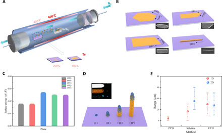
(A) Growth schematic of low-dimensional Te. The light blue and yellow spheres represent the Sn and Te elements, respectively. Te nanosheets and nanowires grow at 400° and 200°C, shown in the enlarged illustration. (B) Schematic diagrams of different morphologies and growth directions. The illustrations in the lower right corner are the corresponding SEM figures. (C) Simulated surface energies for {100}, {010}, {101}, and {001}. The specific value corresponding to each crystal plane. (100): 0.0166 eV/Å2; (010): 0.0166 eV/Å2; (001): 0.0258 eV/Å2; (101): 0.0239 eV/Å2; (10): 0.0237 eV/Å2. (D) Growth process schematics of Te nanowire. (I): Formation of the Sn nanoparticle, (II): Formation of Sn-Te neck with the increasing Te concentration, (III): Growth of Te nanowire, and (IV): Formation of Sn-catalyzed Te. TEM image and energy-dispersive x-ray mappings of Sn-catalyzed Te nanowire are shown in the inset, respectively. STEM, scanning transmission electron microscopy; HAADF, high-angle annular dark field. (E) Dimensional statistics of low-dimensional Te materials synthesized by different methods. Range refers to lengths for nanowires and widths for nanosheets.
In the low-temperature region, the growth of Te nanowires is different from that of Te nanosheets. First, a small amount of Sn would deposit on the substrate. Second, when the growth continues and the precursor vapor arrives at the substrate, SnTe alloy seeds would be formed by the diffusion of Te atoms into the Sn catalyst droplets. Te element has a higher melting point, so Te element in the raw material is easier to deposit than Sn element. As the raw materials feeding the alloy continuously, the Te in the SnTe alloy would be gradually saturated, leading to the epitaxial growth of Te nanowires. The growth energy is low in the area where the nanowires grow. According to the analysis of surface energy, the Te nanowires preferentially grow along the [001] direction. Last, Te nanowires are formed.
The formation of Te nanowires in the low-temperature region of the furnace is dominated by thermodynamics. It is related to the decomposition of Sn from our raw materials SnTe2. To confirm the above nanowire growth process, elemental analysis of the Te nanowires was performed. It is found that Te is uniformly distributed in the whole nanowire, including the axial and radial directions of the nanowires, shown in the inset of Fig. 2D. Sn is obviously accumulated at the top of the nanowire. Energy dispersive spectrometer results further show that the Sn element is dominant at the top of the Te nanowire, and the Sn element only accounts for a very small content in the entire material element composition, as shown in fig. S4A. The results are consistent with the elemental mapping analysis.
The metal Sn is a common catalyst metal for nanowire growth, and the area and ratio of element Sn distributed in our Te nanowires is a typical phenomenon of Sn as a nanowire catalytic metal in the vapor-liquid-solid mechanism (27–29).
Te nanosheets and nanowires are not simply mixed in the same area. There will be obvious morphological differences in different temperature regions. As shown in fig. S6, combined with the growth mechanism mentioned above, only nanowires exist in the low-temperature zone (region A). Te nanosheets in the medium temperature zone (region B) are mostly rectangular as shown in fig. S6C. The nanosheets in the high-temperature region (region C) will more exist with the pentagonal or hexagonal morphology. The growth morphology of Te materials in different temperature zones could be controllable.
Compared to the previous synthesis methods of low-dimensional Te materials, the CVD method is reported here. Figure 2E shows the dimensions of Te materials synthesized by different methods. The length shown in the figure is the lengths for one-dimensional (1D) nanowires and the widths for 2D nanosheets. It can be seen that the sizes of Te materials prepared by CVD, whether it is 1D or quasi-2D, are large in several synthesis methods (30–32). Meanwhile, the CVD method has exhibited the unique potential in large-area and templated growth of the nanowires and 2D materials (33–35), which lays the foundation for further controlled large-area growth of low-dimensional Te materials.
Optoelectronic properties of low-dimensional Te photodetectors
Room-temperature stable infrared detectors are of great significance in a host of fields. Here, we show the potential application of low-dimensional Te in room-temperature infrared detectors. Figure 3A shows the output characteristic curve of the Te nanowire field-effect transistor (FET) device, and the inset is a schematic diagram of the device. Meanwhile, Te nanosheet FET devices were also fabricated. The corresponding transfer characteristic curves, optical microscopy images of different Te devices, are shown in fig. S9. To further confirm the mobility of low-dimensional Te devices, 20 Te devices were fabricated. As shown in fig. S13, one can find that the mobilities of most Te nanowires and nanosheets exceed 100 and 500 cm2 V−1 per second, respectively. Moreover, the mobilities are much higher comparing with other transition metal dichalcogenides (table S1), which is suitable for the preparation of fast devices.
Fig. 3. Electrical and optoelectrical properties of low-dimensional Te devices.
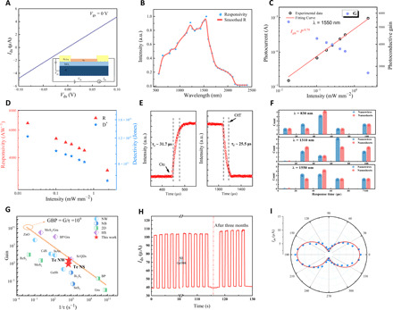
(A) Output characteristic (Vds-Ids) curve of Te nanowire device, exhibiting a good ohmic contact. The inset shows the schematic diagram of the device. (B) Photoresponse spectrum of Te nanowire device under the laser illumination with the wavelength from 500 to 2500 nm and a power intensity of 0.01 mW mm−2. The device operated at a bias of 0.1 V. (C) Photocurrent and photoconductive gain versus power intensity under 1550-nm laser illumination. (D) Responsivity and detectivity versus power intensity under 1550-nm laser illumination. (E) Time-resolved photoresponse of Te nanowire photodetector under 1550-nm laser illumination. (F) Photoresponse time statistics of low-dimensional Te photodetectors at different wavelengths. Ten nanowire and nanosheet devices were tested each. (G) Gain-bandwidth product (GBP) of low-dimensional photodetectors, exhibiting that the high GBP of low-dimensional Te photodetectors. The yellow line represents a typical magnitude order of GBP for traditional thin-film photodetectors, in low-dimensional material systems, except for those hybrid light guides, the values of devices in our work are one of the few ones that are close to this limit. NW, nanowire; NB, nanobelt; NS, nanosheet; HS, hybrid structure. (H) Stability of Te nanowires device. The device was measured at the Vds = 0.1 V. (I) Polarization properties of Te nanosheet photodetectors under 830-nm laser illumination.
The optoelectronic properties of low-dimensional Te photodetector determine the potential of Te as a future room-temperature infrared detector material. Figure 3B shows that the Te nanowire photodetector has a good response to light with a broadband wavelength from 500 to 2500 nm, which agrees well with the absorption spectra of Te. The spectral response of the Te nanosheet device is similar to that of the nanowire device, as shown in fig. S16. In addition, the absorption spectrum and electric field distribution of Te nanosheet and nanowire devices were simulated by the finite difference time domain method. The simulated absorption spectrum of low-dimensional Te photodetectors for different illumination wavelengths was exhibited in fig. S17 (A and C). The simulated curves have significant peaks between 1300 and 1700 nm, which matches the experimental photoresponse of the devices.
The broadband spectral photoresponses of low-dimensional Te photodetectors exhibit the highest response at the wavelength ranging from 1100 to 1500 nm. Therefore, a 1550-nm laser was mainly applied to characterize the optoelectronic performances of the devices in our work. Figure 3C shows that the photocurrent Iph and gain G are closely dependent on the power intensity. The relationship between the photocurrent and intensity could be fitted through a nonlinear function, Iph = cpk, where the c is a proportionality constant, p is the incident laser intensity, and k is an empirical value. In addition, k = 0.79 is acquired, implying that the device under the laser illumination is affected by the photogating effect, electron-hole generation, trapping, and recombination processes (5, 36). In general, the gain G of the devices with photogating effects can be defined as , where Iph is the photocurrent, e is the electronic charge, P is the average power density of the incident light, A is the illuminated area of the device, and hν is the energy of an incident photon. The responsivity R is one of the most important indicators of a photodetector, which can be obtained by . R of Te photodetector under 1550 nm laser illumination is up to 6650 A W−1, shown in Fig. 3D. For both the Te nanowires and nanosheets devices, the gain is dependent on the wavelength of the laser, and the value of gain is relatively low compared to that of other low-dimensional materials, but the responsivity at the wavelength of 1550 nm is one of the best in state-of-the-art low-dimensional materials devices (see table S2), which can be attributed to the good crystal quality of Te materials as well as surface defects. As two other important performance parameters of the photodetector, noise equivalent power (NEP) and detectivity (D*) are affected by the three main types of noise, Johnson noise, 1/f noise, and shot noise from dark current (37). The NEP and D* can be calculated by the equations,, , where R presents the responsivity, 〈in〉2 is the noise current power, A is the effective area of a photodetector, B is the bandwidth. As shown in Fig. 3D, the specific detectivity of Te nanowires photodetector is up to 1.23 × 10¹² Jones at the bias voltage of 0.1 V. Relevant noise power density spectra for Te nanosheets and nanowires are shown in fig. S18. Figure 3D exhibits the obtained R and D* as a function of incident light intensity. As infrared light intensity decreases, both R and D* increase markedly. In addition, the photoresponse speed is a vital parameter for infrared photodetectors. In Fig. 3E, the rise and fall times of the Te nanowire device are 31.7 and 25.5 μs, respectively. Compared with the previously reported devices in table S2, the response time of about 20 μs represents one of the fastest speeds among all the photoconductive infrared detectors reported in the literature. In summary, the responsivity, response time, and detectivity of low-dimensional Te photodetectors are impressive. In addition to the optoelectronic characteristic 1550 nm, the Te nanosheet and nanowire photodetectors under other light illuminations such as 830 nm, 1310 nm, and 2 μm were also characterized. Compared with the performance at 1550 nm, the R and specific D* of Te photodetectors are slightly smaller but still on the same order of magnitude. The statistics of the response time at the different wavelengths (830, 1310, and 1550 nm) are present in Fig. 3F. The response time of Te nanosheet and nanowire photodetectors is relatively stable, most of which are tens of microseconds.
It is well known that there is a trade-off between gain (G) and response time for low-dimensional photoconductive photodetectors (38). Because of the limitation of the τlifetime of the excited photocarrier in the materials, the gain and bandwidth are in a competitive relationship. Without the decay of gain, the maximum bandwidth can be roughly estimated by 1/τ, where τ is the response time. Thus, the gain-bandwidth product (GBP) of each device is constant. The result shows that photodetectors with a larger responsivity often exhibit a slower response speed. The GBP value of the photodetectors is larger, meaning that the performance of the device is closer to the theoretical limit. Figure 3G shows a summary of GBP values for photoconductive detectors. The GBP values of Te nanosheet and nanowire photodetectors are notably higher than that of other photoconductive photodetectors. Moreover, the GBP of low-dimensional Te photodetectors is even comparable to that of the traditional thin-film photodetectors, which is marked by the yellow diagonal line (1 × 10⁹).
Air stability is also very important for low-dimensional photodetectors. All optoelectronic properties of the Te devices were measured under atmospheric conditions at room temperature. Compared to other infrared photodetectors, such as BP, b-AsP, and III-V semiconductor nanowires, the stability of low-dimensional Te devices is very excellent, as displayed in Fig. 3H and figs. S27 and S28. The photoelectric polarization performance of the Te nanosheet device under the 830-nm illumination is shown in Fig. 3I. The extinction ratio of the device at 830 nm can reach ~5.8, while the extinction ratios at 1310 and 1550 nm are 1.3 and 1.6, respectively (see fig. S29). Moreover, the polarization-resolved photocurrent mappings of Te nanosheet photodetector were achieved, shown in fig. S29. It is clear that the photocurrent of Te nanosheet device in the mapping diagram gradually decreases with increasing the polarization angle from 0° to 90°. All the results reveal that low-dimensional Te has great potential for high-sensitive, ultrafast, stable, and broadband infrared photodetectors.
Blackbody detection and imaging of low-dimensional Te photodetectors
Blackbody detection, as a detection standard for practical applications, is used to demonstrate the infrared detection performance of photodetectors. Figure 4A presents the schematic diagram of the blackbody detection system. See Materials and Methods for details. Figure 4B shows the responsivity (R) and detectivity (D*) of low-dimensional Te photodetectors under 1200 K blackbody source illumination. No matter how the frequency of the chopper changes during the measurements, the blackbody responses of the devices are basically maintained at the same level. These results further confirm the stability and large bandwidth of the Te detectors. The R and D* of Te nanowire devices can reach up to 2.53 A W−1 and 4.68 × 10⁸ Jones, respectively. The D* of the Te device under this blackbody temperature condition is slightly higher than that of the carbon tube. Although D* of the Te device is not as good as that of the BP or BP/MoS2 devices, the photodetection of the Te devices can be further improved by preparing a p-n junction or hybrid structure. Combined with the performances under the previous laser measurement conditions, the infrared detection performances of detectors based on Te materials are one of the best among low-dimensional photodetectors. Meanwhile, the detection range can also be widened by material doping.
Fig. 4. Blackbody detection of low-dimensional Te photodetectors.
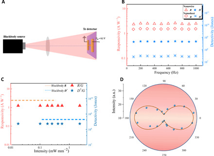
(A) Polarization blackbody measurement schematic of low-dimensional Te photodetectors under blackbody source illumination. After adding the polarizer and half-wave plate, the blackbody polarization measurement can be performed. (B) Blackbody responsivity and detectivity of Te nanowire and nanosheet detectors versus the frequency. (C) Pure responsivity Rp and pure detectivity Dp* versus power intensity under 1550-nm laser illumination. Pure responsivity Rp and pure detectivity Dp* are calculated under laser measurement conditions, corresponding to the triangle and pentagram in the figure, and the blackbody calculation results correspond to the dotted lines, which are unrelated to power intensity. (D) Polarization properties of Te nanosheet photodetector under blackbody source illumination. The polarization angle of the blackbody source is changed by rotating the half-wave plate when the frequency of the chopper is stabilized at 1000 Hz.
Photoconductive gain is usually observed in photoconductive devices under laser irradiation. The high Rlaser and Dlaser* values of photodetectors under laser illumination include the contribution from the gain effect. Thus, the calculated Rlaser and Dlaser* are much larger, compared to the measured values of the commercial photodetectors. To show the smaller gain in blackbody detection of the Te photodetectors, pure responsivity Rp and pure detectivity Dp* eliminating the gain effect are proposed, where and . When we calculated the pure responsivity of the Te photodetectors, the quantum efficiency has defaulted to 1. The pure responsivity Rp is the theoretical maximum responsivity without gain. In addition, the pure detectivity Dp* is calculated under the condition of theoretical maximum responsivity without gain. The pure responsivity Rp and pure detectivity Dp* under the 1550-nm laser can be calculated as 1.25 A W−1 and 2.3 × 10⁸ Jones, respectively, shown in Fig. 4C. Meanwhile, the blackbody peak responsivity of 5.19 A W−1 and detectivity of 9.6 × 10⁸ Jones at the 1550 nm are obtained, respectively. The responsivity Rblackbody and detectivity Dblackbody under blackbody condition are very close to the pure responsivity Rp and pure detectivity Dp*. It means that our device also has a gain in detecting blackbody sources, but it is much smaller than the gain of the laser condition.
The blackbody response of the Te nanosheet device at different polarization angles is shown in Fig. 4D. The extinction ratio of the Te nanosheet device is approximately 2.4. It can be concluded that, because of the excellent anisotropy of the Te crystal, the Te photodetectors exhibit a good photoelectric polarization response under both laser and blackbody illumination.
Among the low-dimensional materials, only a few materials and devices with blackbody response have been reported, as shown in Table 1. Compared with other materials, the stability of low-dimensional Te is better. The synthesis method of CVD is more controllable and has the potential to realize the growth of large-area materials. Meanwhile, low-dimensional Te devices exhibit excellent blackbody response and have the sensitivity of a polarized blackbody source, which provides a novel platform for blackbody detection in the low-dimensional system.
Table 1. Comparison of low-dimensional blackbody-sensitive photodetectors.
b-AsP, black phosphorus-arsenic; CQDs, colloidal quantum dots.
| Material |
Stability (atmosphere) |
Synthesis method |
Controlled growth |
Operating temperature |
Blackbody chopped frequency |
Detectivity (Jones) at morphology |
Polarization extinction ratio |
References |
| BP | <3 days | Mechanical exfoliation |
No | 300 K | 150 Hz | 6 × 10¹⁰ at film (32 nm) |
~ 10 (3.5-μm laser) |
(16) |
| b-AsP | <3 days | Mechanical exfoliation |
No | 300 K | 150 Hz | 2.4 × 10¹⁰ at film (66 nm) |
- | (16) |
| BP/MoS2 | <3 days | Mechanical exfoliation |
No | 300 K | - | 7 × 10⁹ at p-n junction (20 nm) |
~4 (3.5-μm laser) | (9) |
| Carbon nanotube |
>3 months | LPCVD | Yes | 300 K | ~2 Hz | 1.9 × 10⁷ at carbon nanotube forest film (100 μm) |
- | (15) |
| HgTe CQDs | ~1 month | Chemical solution growth |
Yes | 85/295 K | 10 kHz | 3 × 10¹⁰/1 × 107 at npn structures film (1 μm) |
- | (18) |
| Te nanosheet | >3 months | CVD | Yes | 300 K | 1000 Hz | 2.06 × 10⁷ at single nanosheet (85 nm) |
2.4 (blackbody) | This work |
| Te nanowire | >3 months | CVD | Yes | 300 K | 1000 Hz | 4.68 × 10⁸ at single nanowire (diameter ~ 200 nm) |
- |
It can be seen from the above-obtained data that the detectivity of the same device under laser irradiation is much higher than the blackbody peak detectivity at the corresponding wavelength. According to the data analysis of Fig. 4C, it can be inferred that this is related to the gain in low-dimensional Te material. More analysis of the optoelectronic performance data reveals that the gain is dependent on the wavelength, shown in Fig. 5A. As shown in Fig. 3C, gain G decreases as the laser intensity increases. At 1310 nm, 1550 nm, and 2 μm with the same intensity of 0.1 mW mm−1, the specific gain of the same nanowire device is about 1500, 4000, and 500. However, the gain under the blackbody radiation source is approximately 5, which is much smaller than that of the laser.
Fig. 5. Response mechanism of Te nanowire photodetectors under laser and blackbody illumination.
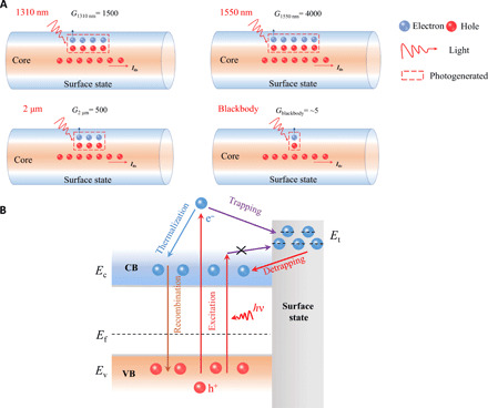
(A) Schematic diagram of the surface state effect of nanowires under different light sources. Under the irradiation of 1310-, 1550-nm, and 2-μm laser and blackbody light source, the ability of surface states to capture photogenerated electrons is different, so the gain caused by the surface states are different, respectively, about 1500, 4000, 500, and 5. (B) Schematic illustration of the defect energy level in the surface state. Et stands for defect energy level. The blackbody source contains photons of various energies, the defect energy level is preferentially occupied by electrons excited by high-energy photons, resulting in a small gain of the blackbody. CB, conduction band; VB, valence band.
For nanowires photodetectors, the gain is not only derived from the intrinsic materials but also affected by the surface state. After illumination, these states will trap one type of photo-generated carriers and continuously form the gate electric field to modulate the channel conductance, resulting in more electron-hole pairs collected by the electrode, which means higher gain devices. These have been extensively and well studied, and especially under laser irradiation, this phenomenon is more obvious (5, 38–41). Combined with the previous TEM characterization, it is obvious that there are plentiful surface states in the Te nanowires and nanosheets, which leads to the high gain of the Te photodetectors. In addition, the schematic diagram of the effect of the surface states in the nanowires is shown in Fig. 5A. The surface states with the defect energy level existing above the conduction band are hindered by a barrier from the channel, as shown in Fig. 5B. Hot electrons excited by high-energy photons have enough energy to overcome the barrier and then be trapped by the defects (42). The process of electrons releasing from the defects to the conduction band is called the detrapping process, which requires thermal assistance to fulfill. The ability of surface states to capture electrons under different lasers is different, depending on the two processes of trapping and detrapping. The photoresponse properties of the device are obtained under 520-, 637-, 830-, 1310-, 1550-nm, and 2-μm laser illumination, as shown in fig. S32. The photocurrent Iph and gain G are closely dependent on power intensity. Figure S31B shows the gain of the same device illuminated by lasers with different wavelengths. The gain of the Te device under 520- and 637-nm lasers is relatively small. For high-energy photons, although the corresponding excited electrons can be easily captured by surface states, they can be efficiently detrapped as well. Thus, a smaller gain is observed for visible light and near-infrared wavelength light.
The simulated 1200 K blackbody spectrum in the Supplementary Materials shows that the energy of most photons is lower than that of the 2-μm laser. However, the higher-energy photons also exist in blackbody sources.
Under the blackbody source illumination, the Te device is simultaneously illuminated by photons of different energies. The defect energy level is preferentially occupied by electrons excited by higher-energy photons (42). Thus, the available surface states for lower-energy photon-induced electrons are reduced, leading to a reduced gain under blackbody illumination compared with laser illumination.
Imaging is a significant application field of photodetectors (43, 44). To check the imaging capability of Te photodetector, a reflection imaging system has been set up, as shown in Fig. 6A. Two sets of objective samples were prepared. The imaging results of the Te nanosheet detectors are shown in Fig. 6 (B and C). The images under both visible and infrared illuminations are very legible. Even some defects of metal objects generated during the fabrication process could be distinguished, such as small gold nuggets in the letter D and the irregular parts in the lower right corner of the institute icon. A series of imagings illustrate the excellent imaging ability of the low-dimensional Te photodetectors.
Fig. 6. Imaging of Te nanosheet photodetectors.
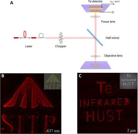
(A) Schematic of the reflection imaging system for Te nanosheet photodetector. (B and C) Imagings by Te nanosheet photodetectors under the wavelength of 637 nm and 2 μm, respectively. The inset shows optical microscopy images of the imaging objective sample. Shanghai Institute of Technical Physics, SITP. (C) “Te,” “INFRARED,” and “HUST.”
Conclusions
In summary, large-scale, high-quality tellurium nanosheets and nanowires have been successfully prepared by CVD. Meanwhile, the growth mechanism of low-dimensional Te is illustrated. Both the ultrahigh hole mobility and good crystallinity ensure the excellent photoresponse performance of the devices based on low-dimensional Te. Low-dimensional Te detectors exhibit excellent performance with a large responsivity (6650 A W−1), a high detectivity (1.23 × 10¹² Jones), and an ultrafast photoresponse (25.5 μs) under the laser illumination. Noticeably, CVD-grown Te detectors have an obvious room-temperature blackbody response. Furthermore, high-resolution imaging by the Te photodetectors has confirmed the great potential of Te in practical application fields. In the future, p-n junction or other hybrid structure devices based on pure Te material can be designed to further improve the photodetection performance of the devices. Meanwhile, flexible substrates or array template substrates can be applied to grow high-quality materials and then make full use of the excellent electrical and photoelectric properties of Te materials in not only photodetectors but also functional and integrated devices.
MATERIALS AND METHODS
Materials synthesis and characterization
The large-area tellurium nanosheets and nanowires were grown via a CVD method. A ceramic boat with SnTe2 powder (Sigma-Aldrich, 99.99%) in it was placed in the middle of a quartz tube. The silicon substrate was placed on another ceramic boat downstream of the carrier gas N2. The flow rate of gas is 50 standard-state cubic centimeters per minute. The SnTe2 in the quartz tube was heated to 650°C. The growth was maintained at atmospheric pressure for 30 min and then naturally cooled down.
The morphologies of tellurium nanosheets and nanowires were investigated by SEM (JEOL Model JSM-6490). HRTEM, SEAD (JEOL JEM-2100F), and XRD patterns ((Bruker D8) were used to characterize the crystal structure. A Bruker Fourier transform infrared spectrometer (Vertex 70v) integrated with a Hyperion 2000 microscope was used to analyze the absorption spectrum of Te. The topography of materials and devices was characterized by AFM (Bruker MultiMode 8).
Polarized Raman studies
Polarization-resolved Raman scattering measurements were recorded every 10° by a micro-Raman spectrometer with backscattering geometry (Jobin-Yvon LabRAM HR Evolution spectrometer). The resolution of spectral is smaller than 1 cm−1, and the wavelength of the excitation source is 532-nm laser. The laser source was focused via a ×100 magnification microscope, and the working distance is 18 mm. The scattered signals are dispersed on 1800 grooves/mm grating, and they are collected through a charge-coupled device, which the front-illuminated chip is 1024 × 256 pixels.
Device fabrication and analysis
All devices were prepared by using the electron-beam lithography technique. Before depositing the contact metal, Te nanowires and nanosheets were immersed in a 3% hydrofluoric acid solution for about 10 s to remove the natural oxide layer. Then, the substrate was immediately put into the thermal evaporation system. The metal contacts with the Te material directly, achieving a good ohmic contact between the metal and Te semiconductor. Pt/Au (50/100 nm) was used as contacted metal for source/drain electrodes; most of the electronic and optoelectronic properties were measured under ambient conditions at room temperature. All I-V (current/voltage) characteristics were measured by the Agilent B2902A source. The laser source for spectral response is provided by the combination of continuous laser light source and gratings. Other laser light sources are emitted from a monochrome laser, which could be any laser wavelength in the 520 nm to 2 μm. High time-resolution response current signal was converted to a voltage signal using a preamp (Stanford Research Systems SR570) and recorded by Tektronix MDO3014 mixed domain oscilloscope.
Blackbody system and analysis
The blackbody source is HFY-206A without a focusing lens. The device was placed 15 cm away from the aperture with a fixed modulation frequency of 1000 Hz chopped by an optical chopper wheel. An 800-nm to 2.7-μm bandpass polarizer and a 1-μm high-pass half-wave plate are placed in front of the device for blackbody polarization measurements. The total incident power on the device surface can be calculated by the approximation formula , where α is the modulation factor, ε is the average emissivity of the blackbody source, ε is 0.9 for our blackbody source, σ is the Stefan-Boltzmann constant. Ts and T0 are the temperature of the blackbody radiation source and the room temperature (300 K), respectively. A is the device area in units of square centimeters. R is the aperture radius of the blackbody radiation source, and L is the distance between the aperture and sample in units of centimeters.
Imaging system and analysis
The light beam emitted by the laser light source is converted into a pulsed beam by a chopper and then reflected by a half mirror and focused on the surface of the imaged object through the objective lens. After being reflected by the object, the laser beam is irradiated onto the detector through the objective lens, a half mirror, and a condensing lens. The electrical signals of the detector are extracted by a lock-in amplifier to obtain the corresponding image. This reflection imaging system is active imaging. The imaging principle is that the light source is irradiated to the surface of the detected object, and the object will reflect the illumination light. For a laser beam of a specific wavelength, different objects have different reflectivity or the same object with different morphologies has different reflectivity, resulting in different reflected light intensities. The system applies the detection device for detecting the change of the reflected beam light intensity, which can reflect the object’s spatial position and shape. Last, the measured object could be reconstructed by plane scanning.
Acknowledgments
We thank M. M. Han, Z. X. Yang, and J. N. Dai for help in the discussion. Funding: This work was supported by the National Natural Science Foundation of China (grant nos. 61725505, 11734016, 61905266, 61904184, 61521005, 62004207, and 31900748), Fund of Shanghai Natural Science Foundation (grant nos. 19XD1404100, 20YF1455900, 19YF1454600, 18ZR1445900, and 18ZR1445800), and special grants from China Postdoctoral Science Foundation (prestation) (grant nos. 2019TQ0333 and 2019TQ0334). Fund of SITP Innovation Foundation (Grant No. CX-348). Author contributions: Z.W., P.W., F.W., and W.H. initiated and supervised the project. M.P. performed device fabrication, data collection, and analysis. Z.W., J.Y., and M.P. deposited Te by CVD. Y.W., P.W., and Q.L. assisted in carrying out the device fabrication and characterizations. W.J., L.Z., J.W., and J.M. assisted in the device performance measurements. Y.Y., Y.L., Z.H., and H.Y. performed part of the Raman, PL, and absorption spectrum characterization. R.X., H.G., X.G., C.S., and X.Z. completed the theoretical calculation part. J.D., C.C., F.W., W.L., and X.C. cowrote the manuscript. All authors discussed the results and commented on the manuscript. Competing interests: The authors declare that they no competing interests. Data and materials availability: All data needed to evaluate the conclusions in the paper are present in the paper and/or the Supplementary Materials. Additional data related to this paper may be requested from the authors.
SUPPLEMENTARY MATERIALS
Supplementary material for this article is available at http://advances.sciencemag.org/cgi/content/full/7/16/eabf7358/DC1
REFERENCES AND NOTES
- 1.F. Parra, P. Meza, C. Toro, S. Torres, Infrared Focal Plane Array Imaging System Characterization by Means of a Blackbody Radiator, in Progress in Pattern Recognition, Image Analysis, Computer Vision, and Applications (Springer-Verlag, 2011), pp. 105–112. [Google Scholar]
- 2.G. Cao, T. Li, H. Tang, X. Shao, X. Li, H. Gong, Performance of extended wavelength InGaAs/InAsP SWIR detector, in 7th International Symposium on Advanced Optical Manufacturing and Testing Technologies, Y. Jiang, J. Yu, B. Kippelen, Eds. (SPIE, 2014), vol. 9284, chap. 1. [Google Scholar]
- 3.Camargo E. G., Ueno K., Kawakami Y., Moriyasu Y., Nagase K., Satou M., Endo H., Ishibashi K., Kuze N., Miniaturized InSb photovoltaic infrared sensor operating at room temperature. Opt. Eng. 47, 014402 (2008). [Google Scholar]
- 4.McCullough P. R., Regan M., Bergeron L., Lindsay K., Quantum efficiency and quantum yield of an HgCdTe infrared sensor array. Publ. Astron. Soc. Pac. 120, 759–776 (2008). [Google Scholar]
- 5.Guo N., Hu W., Liao L., Yip S. P., Ho J. C., Miao J., Zhang Z., Zou J., Jiang T., Wu S., Chen X., Lu W., Anomalous and highly efficient InAs nanowire phototransistors based on majority carrier transport at room temperature. Adv. Mater. 26, 8203–8209 (2014). [DOI] [PubMed] [Google Scholar]
- 6.Liu C.-H., Chang Y.-C., Norris T. B., Zhong Z., Graphene photodetectors with ultra-broadband and high responsivity at room temperature. Nat. Nanotechnol. 9, 273–278 (2014). [DOI] [PubMed] [Google Scholar]
- 7.Wang J. L., Fang H., Wang X., Chen X., Lu W., Hu W., Recent progress on localized field enhanced two-dimensional material photodetectors from ultraviolet-visible to infrared. Small 13, 1700894 (2017). [DOI] [PubMed] [Google Scholar]
- 8.Long M., Wang Y., Wang P., Zhou X., Xia H., Luo C., Huang S., Zhang G., Yan H., Fan Z., Wu X., Chen X., Lu W., Hu W., Palladium diselenide long-wavelength infrared photodetector with high sensitivity and stability. ACS Nano 13, 2511–2519 (2019). [DOI] [PubMed] [Google Scholar]
- 9.Bullock J., Amani M., Cho J., Chen Y.-Z., Ahn G. H., Adinolfi V., Shrestha V. R., Gao Y., Crozier K. B., Chueh Y.-L., Javey A., Polarization-resolved black phosphorus/molybdenum disulfide mid-wave infrared photodiodes with high detectivity at room temperature. Nat. Photonics 12, 601–607 (2018). [Google Scholar]
- 10.Peres N. M. R., Santos J. E., Strong light-matter interaction in systems described by a modified Dirac equation. J. Phys. Condens. Matter 25, 305801 (2013). [DOI] [PubMed] [Google Scholar]
- 11.Zhou C., Zhang X.-T., Zheng K., Chen P.-P., Lu W., Zou J., Correction to Self-assembly growth of In-rich InGaAs core-shell structured nanowires with remarkable near-infrared photoresponsivity. Nano Lett. 19, 2188–2188 (2019). [DOI] [PubMed] [Google Scholar]
- 12.Liang Q., Wang Q., Zhang Q., Wei J., Lim S. X., Zhu R., Hu J., Wei W., Lee C., Sow C. H., Zhang W., Wee A. T. S., High-performance, room temperature, ultra-broadband photodetectors based on air-stable PdSe2. Adv. Mater. 31, 1807609 (2019). [DOI] [PubMed] [Google Scholar]
- 13.Youngblood N., Chen C., Koester S. J., Li M., Waveguide-integrated black phosphorus photodetector with high responsivity and low dark current. Nat. Photonics 9, 247–252 (2015). [Google Scholar]
- 14.Liu Y., Shivananju B. N., Wang Y., Zhang Y., Yu W., Xiao S., Sun T., Ma W., Mu H., Lin S., Zhang H., Lu Y., Qiu C.-W., Li S., Bao Q., Highly efficient and air-stable infrared photodetector based on 2D layered graphene-black phosphorus heterostructure. ACS Appl. Mater. Interfaces 9, 36137–36145 (2017). [DOI] [PubMed] [Google Scholar]
- 15.Zhang M., Ban D., Xu C., Yeow J. T. W., Large-area and broadband thermoelectric infrared detection in a carbon nanotube black-body absorber. ACS Nano 13, 13285–13292 (2019). [DOI] [PubMed] [Google Scholar]
- 16.Amani M., Regan E., Bullock J., Ahn G. H., Javey A., Mid-wave infrared photoconductors based on black phosphorus-arsenic alloys. ACS Nano 11, 11724–11731 (2017). [DOI] [PubMed] [Google Scholar]
- 17.McDonald S. A., Konstantatos G., Zhang S., Cyr P. W., Klem E. J. D., Levina L., Sargent E. H., Solution-processed PbS quantum dot infrared photodetectors and photovoltaics. Nat. Mater. 4, 138–142 (2005). [DOI] [PubMed] [Google Scholar]
- 18.Tang X., Ackerman M. M., Chen M., Guyot-Sionnest P., Dual-band infrared imaging using stacked colloidal quantum dot photodiodes. Nat. Photonics 13, 277–282 (2019). [Google Scholar]
- 19.Fang H., Wu P., Wang P., Zheng Z., Tang Y., Ho J. C., Chen G., Wang Y., Shan C., Cheng X., Zhang J., Hu W., Global photocurrent generation in phototransistors based on single-walled carbon nanotubes toward highly sensitive infrared detection. Adv. Opt. Mater. 7, 1900597 (2019). [Google Scholar]
- 20.Lin Z.-H., Yang Z., Chang H.-T., Preparation of fluorescent tellurium nanowires at room temperature. Cryst. Growth Des. 8, 351–357 (2008). [Google Scholar]
- 21.Talapin D. V., Shevchenko E. V., Bodnarchuk M. I., Ye X., Chen J., Murray C. B., Quasicrystalline order in self-assembled binary nanoparticle superlattices. Nature 461, 964–967 (2009). [DOI] [PubMed] [Google Scholar]
- 22.Löwe K., Liu J., Skokov K., Moore J. D., Sepehri-Amin H., Hono K., Katter M., Gutfleisch O., The effect of the thermal decomposition reaction on the mechanical and magnetocaloric properties of La(Fe,Si,Co)13. Acta Mater. 60, 4268–4276 (2012). [Google Scholar]
- 23.Pechenyuk S. I., Domonov D. P., Gosteva A. N., Kadyrova G. I., Kalinnikov V. T., Synthesis, properties, and thermal decomposition of compounds [Co(En)3][Fe(CN)6]·2H2O and [Co(En)3]4[Fe(CN)6]3·15H2O. Russ. J. Coord. Chem. 38, 596–603 (2012). [Google Scholar]
- 24.Peev N. S., Another look on wulff construction. Cryst. Res. Technol. 52, 1700100 (2017). [Google Scholar]
- 25.Gu Y., Cai H., Dong J., Yu Y., Hoffman A. N., Liu C., Oyedele A. D., Lin Y.-C., Ge Z., Puretzky A. A., Duscher G., Chisholm M. F., Rack P. D., Rouleau C. M., Gai Z., Meng X., Ding F., Geohegan D. B., Xiao K., Two-dimensional palladium diselenide with strong in-plane optical anisotropy and high mobility grown by chemical vapor deposition. Adv. Mater. 32, 2003751 (2020). [DOI] [PubMed] [Google Scholar]
- 26.Zou Y., Chen Z., Lin J., Zhou X., Lu W., Drennan J., Zou J., Morphological control of SnTe nanostructures by tuning catalyst composition. Nano Res. 8, 3011–3019 (2015). [Google Scholar]
- 27.Hu J., Ouyang M., Yang P., Lieber C. M., Controlled growth and electrical properties of heterojunctions of carbon nanotubes and silicon nanowires. Nature 399, 48–51 (1999). [Google Scholar]
- 28.Wu Y., Yang P., Direct observation of vapor-liquid-solid nanowire growth. J. Am. Chem. Soc. 123, 3165–3166 (2001). [Google Scholar]
- 29.Sun R., Jacobsson D., Chen I.-J., Nilsson M., Thelander C., Lehmann S., Dick K. A., Sn-seeded GaAs nanowires as self-assembled radial p-n junctions. Nano Lett. 15, 3757–3762 (2015). [DOI] [PMC free article] [PubMed] [Google Scholar]
- 30.Wang Y., Qiu G., Wang R., Huang S., Wang Q., Liu Y., Du Y., Goddard W. A. III, Kim M. J., Xu X., Ye P. D., Wu W., Field-effect transistors made from solution-grown two-dimensional tellurene. Nat. Electron. 1, 228–236 (2018). [Google Scholar]
- 31.Amani M., Tan C., Zhang G., Zhao C., Bullock J., Song X., Kim H., Shrestha V. R., Gao Y., Crozier K. B., Scott M., Javey A., Solution-synthesized high-mobility tellurium nanoflakes for short-wave infrared photodetectors. ACS Nano 12, 7253–7263 (2018). [DOI] [PubMed] [Google Scholar]
- 32.Qian H.-S., Yu S.-H., Gong J.-Y., Luo L.-B., Fei L.-f., High-quality luminescent tellurium nanowires of several nanometers in diameter and high aspect ratio synthesized by a poly (vinyl pyrrolidone)-assisted hydrothermal process. Langmuir 22, 3830–3835 (2006). [DOI] [PubMed] [Google Scholar]
- 33.Jeon J., Jang S. K., Jeon S. M., Yoo G., Jang Y. H., Park J.-H., Lee S., Layer-controlled CVD growth of large-area two-dimensional MoS2 films. Nanoscale 7, 1688–1695 (2015). [DOI] [PubMed] [Google Scholar]
- 34.Dathbun A., Kim Y., Kim S., Yoo Y., Kang M. S., Lee C., Cho J. H., Large-area CVD-grown sub-2 V ReS2 transistors and logic gates. Nano Lett. 17, 2999–3005 (2017). [DOI] [PubMed] [Google Scholar]
- 35.Zhou H., Yu W. J., Liu L., Cheng R., Chen Y., Huang X., Liu Y., Wang Y., Huang Y., Duan X., Chemical vapour deposition growth of large single crystals of monolayer and bilayer graphene. Nat. Commun. 4, 2096 (2013). [DOI] [PubMed] [Google Scholar]
- 36.Peng M., Wu F., Wang Z., Wang P., Gong F., Long M., Chen C., Dai J., Hu W., Enhancement-mode CdS nanobelts field effect transistors and phototransistors with HfO2 passivation. Appl. Phys. Lett. 114, 111103 (2019). [Google Scholar]
- 37.Gong X., Tong M., Xia Y., Cai W., Moon J. S., Cao Y., Yu G., Shieh C.-L., Nilsson B., Heeger A. J., High-detectivity polymer photodetectors with spectral response from 300 nm to 1450 nm. Science 325, 1665–1667 (2009). [DOI] [PubMed] [Google Scholar]
- 38.Fang H., Hu W., Photogating in low dimensional photodetectors. Adv. Sci. 4, 1700323 (2017). [DOI] [PMC free article] [PubMed] [Google Scholar]
- 39.Yang Y., Peng X., Kim H.-S., Kim T., Jeon S., Kang H. K., Choi W., Song J., Doh Y.-J., Yu D., Hot carrier trapping induced negative photoconductance in InAs nanowires toward novel nonvolatile memory. Nano Lett. 15, 5875–5882 (2015). [DOI] [PubMed] [Google Scholar]
- 40.Furchi M. M., Polyushkin D. K., Pospischil A., Mueller T., Mechanisms of photoconductivity in atomically thin MoS2. Nano Lett. 14, 6165–6170 (2014). [DOI] [PubMed] [Google Scholar]
- 41.Island J. O., Blanter S. I., Buscema M., van der Zant H. S. J., Castellanos-Gomez A., Gate controlled photocurrent generation mechanisms in high-gain In2Se3 phototransistors. Nano Lett. 15, 7853–7858 (2015). [DOI] [PubMed] [Google Scholar]
- 42.Fang H., Hu W., Wang P., Guo N., Luo W., Zheng D., Gong F., Luo M., Tian H., Zhang X., Luo C., Wu X., Chen P., Liao L., Pan A., Chen X., Lu W., Visible light-assisted high-performance mid-infrared photodetectors based on single InAs nanowire. Nano Lett. 16, 6416–6424 (2016). [DOI] [PubMed] [Google Scholar]
- 43.Wang P., Liu S., Luo W., Fang H., Gong F., Guo N., Chen Z.-G., Zou J., Huang Y., Zhou X., Wang J., Chen X., Lu W., Xiu F., Hu W., Arrayed van der waals broadband detectors for dual-band detection. Adv. Mater. 26, 1604439 (2017). [DOI] [PubMed] [Google Scholar]
- 44.Kuo W.-S., Chang C.-N., Chang Y.-T., Yang M.-H., Chien Y.-H., Chen S.-J., Yeh C.-S., Gold nanorods in photodynamic therapy, as hyperthermia agents, and in near-infrared optical imaging. Angew. Chem. Int. Ed. 49, 2711–2715 (2010). [DOI] [PubMed] [Google Scholar]
- 45.Wang Y., Xiao C., Chen M., Hua C., Zou J., Wu C., Jiang J., Yang S. A., Lu Y., Ji W., Two-dimensional ferroelectricity and switchable spin-textures in ultra-thin elemental Te multilayers. Mater. Horiz. 5, 521–528 (2018). [Google Scholar]
- 46.Kresse G., Furthmüller J., Efficient iterative schemes for ab initio total-energy calculations using a plane-wave basis set. Phys. Rev. B. 54, 11169–11186 (1996). [DOI] [PubMed] [Google Scholar]
- 47.Kresse G., Furthmüller J., Efficiency of ab-initio total energy calculations for metals and semiconductors using a plane-wave basis set. Comput. Mater. Sci. 6, 15–50 (1996). [Google Scholar]
- 48.Blöchl P. E., Projector augmented-wave method. Phys. Rev. B. 50, 17953–17979 (1994). [DOI] [PubMed] [Google Scholar]
- 49.Perdew J. P., Burke K., Ernzerhof M., Generalized gradient approximation made simple. Phys. Rev. Lett. 77, 3865–3868 (1996). [DOI] [PubMed] [Google Scholar]
- 50.Grimme S., Semiempirical GGA-type density functional constructed with a long-range dispersion correction. J. Comput. Chem. 27, 1787–1799 (2006). [DOI] [PubMed] [Google Scholar]
- 51.V. Wang, N. Xu, J. C. Liu, G. Tang, W.-T. Geng, VASPKIT: A User-friendly Interface Facilitating High-throughput Computing and Analysis Using VASP Code. arXiv:1908.08269 (2019).
- 52.Zhang Z., Mannix A. J., Liu X., Hu Z., Guisinger N. P., Hersam M. C., Yakobson B. I., Near-equilibrium growth from borophene edges on silver. Sci. Adv. 5, eaax0246 (2019). [DOI] [PMC free article] [PubMed] [Google Scholar]
- 53.Cao D., Shen T., Liang P., Chen X., Shu H., Role of chemical potential in flake shape and edge properties of monolayer MoS2. J. Phys. Chem. C 119, 4294–4301 (2015). [Google Scholar]
- 54.Ye L., Wang P., Luo W., Gong F., Liao L., Liu T., Tong L., Zang J., Xu J., Hu W., Highly polarization sensitive infrared photodetector based on black phosphorus-on-WSe2 photogate vertical heterostructure. Nano Energy 37, 53–60 (2017). [Google Scholar]
- 55.Hämäläinen J., Mattinen M., Mizohata K., Meinander K., Vehkamäki M., Räisänen J., Ritala M., Leskelä M., Atomic layer deposition of rhenium disulfide. Adv. Mater. 30, 1703622 (2018). [DOI] [PubMed] [Google Scholar]
- 56.Yang L., Majumdar K., Liu H., Du Y., Wu H., Hatzistergos M., Hung P. Y., Tieckelmann R., Tsai W., Hobbs C., Ye P. D., Chloride molecular doping technique on 2D materials: WS2 and MoS2. Nano Lett. 14, 6275–6280 (2014). [DOI] [PubMed] [Google Scholar]
- 57.Liu H., Neal A. T., Ye P. D., Channel length scaling of MoS2 MOSFETs. ACS Nano 6, 8563–8569 (2012). [DOI] [PubMed] [Google Scholar]
- 58.Zhang Z., Li T., Wu Y., Jia Y., Tan C., Xu X., Wang G., Lv J., Zhang W., He Y., Pei J., Ma C., Li G., Xu H., Shi L., Peng H., Li H., Truly concomitant and independently expressed short- and long-term plasticity in a Bi2O2Se-based three-terminal memristor. Adv. Mater. 31, 1805769 (2019). [DOI] [PubMed] [Google Scholar]
- 59.Liu H., Neal A. T., Zhu Z., Luo Z., Xu X., Tománek D., Ye P. D., Phosphorene: An unexplored 2D semiconductor with a high hole mobility. ACS Nano 8, 4033–4041 (2014). [DOI] [PubMed] [Google Scholar]
- 60.Li L., Yu Y., Ye G. J., Ge Q., Ou X., Wu H., Feng D., Chen X. H., Zhang Y., Black phosphorus field-effect transistors. Nat. Nanotechnol. 9, 372–377 (2014). [DOI] [PubMed] [Google Scholar]
- 61.Abderrahmane A., Ko P. J., Thu T. V., Ishizawa S., Takamura T., Sandhu A., High photosensitivity few-layered MoSe2 back-gated field-effect phototransistors. Nanotechnology 25, 365202 (2014). [DOI] [PubMed] [Google Scholar]
- 62.Wang Z., Wang P., Wang F., Ye J., He T., Wu F., Peng M., Wu P., Chen Y., Zhong F., Xie R., Cui Z., Shen L., Zhang Q., Gu L., Luo M., Wang Y., Chen H., Zhou P., Pan A., Zhou X., Zhang L., Hu W., A noble metal dichalcogenide for high-performance field-effect transistors and broadband photodetectors. Adv. Funct. Mater. 30, 1907945 (2020). [Google Scholar]
- 63.Sun J., Peng M., Zhang Y., Zhang L., Peng R., Miao C., Liu D., Han M., Feng R., Ma Y., Dai Y., He L., Shan C., Pan A., Hu W., Yang Z.-x., Ultrahigh hole mobility of Sn-catalyzed GaSb nanowires for high speed infrared photodetectors. Nano Lett. 19, 5920–5929 (2019). [DOI] [PubMed] [Google Scholar]
- 64.Miao J., Hu W., Guo N., Lu Z., Zou X., Liao L., Shi S., Chen P., Fan Z., Ho J. C., Li T.-X., Chen X. S., Lu W., Single InAs nanowire room-temperature near-infrared photodetectors. ACS Nano 8, 3628–3635 (2014). [DOI] [PubMed] [Google Scholar]
- 65.Zhou G., Addou R., Wang Q., Honari S., Cormier C. R., Cheng L., Yue R., Smyth C. M., Laturia A., Kim J., Vandenberghe W. G., Kim M. J., Wallace R. M., Hinkle C. L., High-mobility helical tellurium field-effect transistors enabled by transfer-free, low-temperature direct growth. Adv. Mater. 30, 1803109 (2018). [DOI] [PubMed] [Google Scholar]
- 66.Ali H., Zhang Y., Tang J., Peng K., Sun S., Sun Y., Song F., Falak A., Wu S., Qian C., Wang M., Zuo Z., Jin K.-J., Sanchez A. M., Liu H., Xu X., High-responsivity photodetection by a self-catalyzed phase-pure p-GaAs nanowire. Small 14, 1704429 (2018). [DOI] [PubMed] [Google Scholar]
- 67.Zheng D., Wang J., Hu W., Liao L., Fang H., Guo N., Wang P., Gong F., Wang X., Fan Z., Wu X., Meng X., Chen X., Lu W., When nanowires meet ultrahigh ferroelectric field-high-performance full-depleted nanowire photodetectors. Nano Lett. 16, 2548–2555 (2016). [DOI] [PubMed] [Google Scholar]
- 68.Li D., Lan C., Manikandan A., Yip S. P., Zhou Z., Liang X., Shu L., Chueh Y.-L., Han N., Ho J. C., Ultra-fast photodetectors based on high-mobility indium gallium antimonide nanowires. Nat. Commun. 10, 1664 (2019). [DOI] [PMC free article] [PubMed] [Google Scholar]
- 69.Zhou X., Hu X., Jin B., Yu J., Liu K., Li H., Zhai T., Highly anisotropic GeSe nanosheets for phototransistors with ultrahigh photoresponsivity. Adv. Sci. 5, 1800478 (2018). [DOI] [PMC free article] [PubMed] [Google Scholar]
- 70.Huang M., Wang M., Chen C., Ma Z., Li X., Han J., Wu Y., Broadband black-phosphorus photodetectors with high responsivity. Adv. Mater. 28, 3481–3485 (2016). [DOI] [PubMed] [Google Scholar]
- 71.Xia F., Mueller T., Lin Y.-m., Valdes-Garcia A., Avouris P., Ultrafast graphene photodetector. Nat. Nanotechnol. 4, 839–843 (2009). [DOI] [PubMed] [Google Scholar]
- 72.Kufer D., Konstantatos G., Highly sensitive, encapsulated MoS2 photodetector with gate controllable gain and speed. Nano Lett. 15, 7307–7313 (2015). [DOI] [PubMed] [Google Scholar]
- 73.Lai J., Liu X., Ma J., Wang Q., Zhang K., Ren X., Liu Y., Gu Q., Zhuo X., Lu W., Wu Y., Li Y., Feng J., Zhou S., Chen J.-H., Sun D., Anisotropic broadband photoresponse of layered type-II Weyl semimetal MoTe2. Adv. Mater. 30, 1707152 (2018). [DOI] [PubMed] [Google Scholar]
- 74.Yu X., Yu P., Wu D., Singh B., Zeng Q., Lin H., Zhou W., Lin J., Suenaga K., Liu Z., Wang Q. J., Atomically thin noble metal dichalcogenide: A broadband mid-infrared semiconductor. Nat. Commun. 9, 1545 (2018). [DOI] [PMC free article] [PubMed] [Google Scholar]
- 75.Tong L., Huang X., Wang P., Ye L., Peng M., An L., Sun Q., Zhang Y., Yang G., Li Z., Zhong F., Wang F., Wang Y., Motlag M., Wu W., Cheng G. J., Hu W., Stable mid-infrared polarization imaging based on quasi-2D tellurium at room temperature. Nat. Commun. 11, 2308 (2020). [DOI] [PMC free article] [PubMed] [Google Scholar]
- 76.Sun Z., Liu Z., Li J., Tai G.-A., Lau S.-P., Yan F., Infrared photodetectors based on CVD-grown graphene and PbS quantum dots with ultrahigh responsivity. Adv. Mater. 24, 5878–5883 (2012). [DOI] [PubMed] [Google Scholar]
- 77.Roy K., Padmanabhan M., Goswami S., Sai T. P., Ramalingam G., Raghavan S., Ghosh A., Graphene-MoS2 hybrid structures for multifunctional photoresponsive memory devices. Nat. Nanotechnol. 8, 826–830 (2013). [DOI] [PubMed] [Google Scholar]
- 78.Wu F., Li Q., Wang P., Xia H., Wang Z., Wang Y., Luo M., Chen L., Chen F., Miao J., Chen X., Lu W., Shan C., Pan A., Wu X., Ren W., Jariwala D., Hu W., High efficiency and fast van der Waals hetero-photodiodes with a unilateral depletion region. Nat. Commun. 10, 4663 (2019). [DOI] [PMC free article] [PubMed] [Google Scholar]
Associated Data
This section collects any data citations, data availability statements, or supplementary materials included in this article.
Supplementary Materials
Supplementary material for this article is available at http://advances.sciencemag.org/cgi/content/full/7/16/eabf7358/DC1