Abstract
Photodetectors based on transition metal dichalcogenides (TMDs) have been widely reported in the literature and molybdenum disulfide (MoS2) has been the most extensively explored for photodetection applications. The properties of MoS2, such as direct band gap transition in low dimensional structures, strong light–matter interaction and good carrier mobility, combined with the possibility of fabricating thin MoS2 films, have attracted interest for this material in the field of optoelectronics. In this work, MoS2-based photodetectors are reviewed in terms of their main performance metrics, namely responsivity, detectivity, response time and dark current. Although neat MoS2-based detectors already show remarkable characteristics in the visible spectral range, MoS2 can be advantageously coupled with other materials to further improve the detector performance Nanoparticles (NPs) and quantum dots (QDs) have been exploited in combination with MoS2 to boost the response of the devices in the near ultraviolet (NUV) and infrared (IR) spectral range. Moreover, heterostructures with different materials (e.g., other TMDs, Graphene) can speed up the response of the photodetectors through the creation of built-in electric fields and the faster transport of charge carriers. Finally, in order to enhance the stability of the devices, perovskites have been exploited both as passivation layers and as electron reservoirs.
Keywords: MoS2, TMD, photodetector, heterostructure, thin film
1. Introduction
Recent improvements in optoelectronics have been partly focused on the use of two-dimensional materials to produce photodetectors. The possibility of fabricating very thin optoelectronic devices, having high performance, low production costs and mechanical flexibility has been emerging in the last decade. Graphene was the first 2D material considered for photodetection applications, thanks to its outstanding electrical properties, in particular its impressive planar mobility, reaching 200,000 cm2/(V s), that allows to build photodetectors with bandwidth up to 40 GHz [1,2]. However, one of its mayor limitation for its use as photodetector active layer is the absence of an energy band gap, leading to high noise contribution to the signal, arising from dark currents.
Therefore, the investigation of 2D materials with finite bandgap has increased in recent years and transition metal dichalcogenides (TMDs) have aroused more and more interest. Despite the modest mobility reported for these materials, which can reach about 200 cm2/(V s) [3], TMDs possess interesting electro-optical properties. A transition from indirect to direct bandgap has been observed in TMDs by reducing the dimensions from the bulk material to the monolayer limit [4]. Moreover, a strong light–matter interaction is observed for 2D-TMDs, due to the direct band gap and to the strong excitonic nature of their low dimensional structures. For TMDs, absorbance values that are one order of magnitude higher than Si and GaAs are reported [5], thus providing strong light absorption with a very thin layer of the photoactive material. These features, combined with a higher mechanical flexibility of 2D-TMDs compared to their bulk structures, allow us to fabricate very thin photodetectors also based on flexible substrates, opening the possibility to realize flexible and wearable devices. Applications for such devices can be related to medicine, biosensing, optical communications and security.
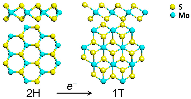
Among the TMDs, molybdenum disulfide (MoS2) attracted much interest in the last decade, also due to the relative abundance of molybdenite in nature. MoS2 belongs to the family of the group VI transition metal dichalcogenides, where a layer of transition metal atoms (Mo, W) is sandwiched between two layers of chalcogen atoms (S, Se, Te) as depicted in Figure 1.
Figure 1.
Transformation of the hexagonal 2H polymorph of MoS2 into its 1T phase, through electron transfer. Reprinted with permission from ref. [6]. © 2017 AIP Publishing.
Each MoS2 layer is generally stacked onto each other via weak van der Waals forces in an ABA stacking sequence, building a hexagonal structure (2H-TMD), which possesses a semiconducting behaviour. Another metastable phase of MoS2 is known, with a tetragonal symmetry (1T-MoS2) and ABC stacking sequence (Figure 1). The 1T phase of MoS2 is not stable at room temperature [7], but it can be induced by several processes such as chemical treatment [8], plasmonic hot electron transfer [9], electron beam irradiation [6,10], through charge transfer in the TMD lattice. A subsequent annealing process is then required to restore the 2H-MoS2 phase [6].
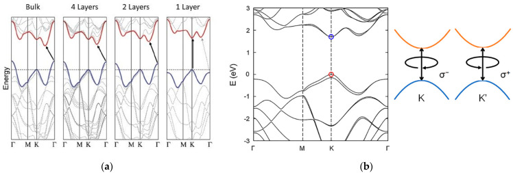
Bulk TMD electronic properties are dominated by indirect transition from the maximum of the valence band, located at the Γ point of the Brillouin zone, and the minimum of the conduction band [11,12,13]. For MoS2, the bulk electronic structure is characterized by an indirect energy band gap of about 1.2 eV [14]. As with other group VI TMDs, at the monolayer limit MoS2 modifies its energy band structure towards a direct electronic transition from the K and K’ points of the Brillouin zone, reaching an energy band gap of 1.8 eV [14,15]. This behaviour can be explained by an increase in the indirect band gap due to a considerable quantum confinement effect in the out-of-plane direction when the dimensions of the material are reduced to few layers. On the other hand, the direct transition remains unaffected, becoming the minimum energetic band-to-band transition [11,12,13] (Figure 2a). Moreover, TMDs are reported to have strong spin-orbit coupling (SOC), associated with the d-orbitals of transition metals [6,16,17]. The SOC breaks the degeneracy in the valence band, leading to two energetic maxima located at the K and K’ points, separated by an energy splitting of 160 meV for a monolayer MoS2 [16] (Figure 2b). This broken degeneracy opens for MoS2 the possibility for optoelectronic applications in the field of valleytronics [18,19].
Figure 2.
Energetic band structure of MoS2. (a) Transition from indirect to direct band gap moving from the bulk MoS2 to the single layer of MoS2. Reprinted with permission from ref. [15]. © 2010, American Chemical Society. (b) Degeneracy at the K point in the valence band of a single MoS2 layer. Reprinted with permission from ref. [6]. © 2017, AIP Publishing.
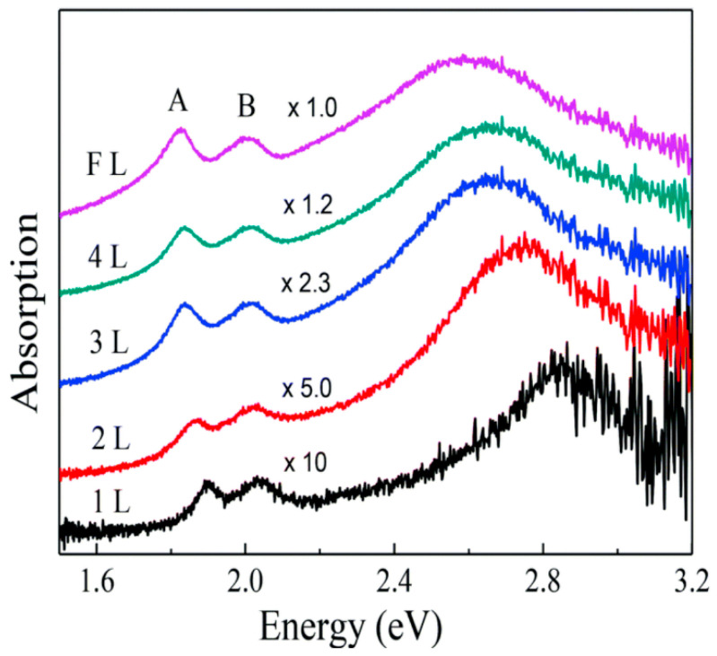
When MoS2 is irradiated with photon energies larger than its bandgap, photons are absorbed and electrons are promoted to the conduction band, leaving holes in the valence band. The optical absorption of visible light by MoS2 in the monolayer limit is dominated by the direct transition from the K and K’ points of the valence band. However, light absorption experiments show peculiar resonant features in 2D structures of MoS2 (Figure 3), that can be associated with its strong excitonic nature [4,15]. The experimentally observed absorption peaks at specific energies (EA = 1.88 eV, EB = 2.03 eV in the monolayer limit [20]) represent the excitonic energies of MoS2. The relative positions of the A and B peaks are related both to an increase in the SOC and to a reduction in the bandgap, approaching the bulk structure of MoS2 [20].
Figure 3.
Absorption spectrum of MoS2 varying the number of layers from 1 layer (1L) to few layers (FL), where A and B represent the excitonic peaks of MoS2. Reprinted with permission from ref. [20]. 2014, Creative Commons Attribution 3.0 Unported Licence.
For these reasons, in 2D-MoS2, the bandgap measured with optical techniques turns out to be lower than the one measured with electronic techniques [6]. The strong light–matter interaction that characterizes MoS2 is reflected in a high absorption coefficient that can reach about 106/cm [21], which is at least one order of magnitude higher than standard semiconductors like Si and GaAs. Moreover, a single MoS2 layer is reported to absorb up to 10% of the sunlight [5]. This superior light absorption makes MoS2 suitable to build photodetectors based on very thin layers of material, still having high light conversion efficiency.
Therefore, the production of thin MoS2 films is a central step of the device fabrication and several approaches have been investigated so far. Thanks to the weak van der Waals interaction between MoS2 layers, it is possible to obtain mono- or few-layered structures by a simple mechanical exfoliation of bulk MoS2 [22]. This approach has been extensively used in many studies [23,24,25,26,27,28,29,30,31,32,33,34,35,36] for its intrinsic simplicity, but suffers from some critical issues. In fact, MoS2 mechanical exfoliation generally leads to very small flakes (lateral size < 10 um) [37] and it is a low yield process. Therefore, it is unsuitable for industrially scalable-applications [38]. Other synthesis methods have been investigated to overcome these critical aspects. Chemical vapour deposition (CVD) is a powerful bottom-up approach. This method is the most compatible with the existing semiconductor technology. In CVD, large area films with high uniformity can be grown directly on the substrate, through the chemical reactions involved in the process. Despite the high controllability of the process and the high uniformity that can be achieved, CVD has the limit of being a costly process and requires high temperatures (700–1000 °C), making the process less affordable and not suitable for deposition on flexible substrates. Moreover, in most of the CVD processes used to produce MoS2, one of the precursors involved is H2S, which is toxic. As an alternative to standard CVD, plasma-enhanced CVD (PECVD) has also been exploited in order to reduce the temperature needed for the reaction (150–300 °C), thus allowing film deposition also on plastic substrates [39].
Among the bottom-up approaches, wet chemical syntheses can also be exploited for the fabrication of large area MoS2 films on different substrates. MoS2 sols can be prepared both at ambient pressure or under hydrothermal [40] or solvothermal [41] synthesis conditions. The sols can be used for coating different substrates by spin-coating or dip-coating. Generally, an annealing process (at 500–800 °C) is required in order to improve the crystallinity of the sample and an additional sulphurisation step is needed. Recently, Nardi et al. [42] have obtained MoS2 thin layers on Pt, SiO2 and flexible polyimide substrates by the sol–gel approach, using an aqueous sol prepared at ambient pressure; the coatings were annealed at low temperature (350–400 °C) without any additional sulphurisation process.
The advantages of the solution methods are represented by the versatility of the deposition technique, the low costs of production and the process scalability. The drawbacks with respect to CVD are instead the lower uniformity of the film and its minimum thickness, which is generally limited to some tens of nanometres.
The fabrication methods cited above generally lead to n-type behaviour of MoS2. The n-type character of pristine MoS2 is commonly associated to the electron donor nature of the sulphur atoms [43]. In order to exploit the full potential of MoS2 and to build p–n junctions, doping is required to tune the energetic levels at the interface of MoS2 with other materials. Doping through standard ion implantation is not suitable for 2D materials, and other methods have been investigated in the literature. The most common methods for doping MoS2 rely on substitutional doping and surface doping, beside the electrostatic gating. Substitutional doping consists of the substitution of a sulphur atom with an impurity within the MoS2 lattice. Niobium (Nb) substitutional p-doping has been reported in the literature by both chemical vapour transport (CVT) [43] and CVD [44]. Moreover, laser assisted substitutional phosphorous (P) p-doping was reported in [45] and manganese (Mn) substitutional p-doping has been investigated in [46], via a vapour phase deposition technique. Finally, p-type substitutions with fluorine (F) and oxygen (O) were obtained via plasma assisted doping by [47]. On the other hand, surface doping exploits the difference between the electron surface potential of MoS2 and the redox potential of the chemically adsorbed species. Nicotinamide adenine dinucleotide (NADH) has been reported to cause an n-doping to MoS2, while tetrafluoro-tetracyanoquinodimethane (F4-TCNQ) and 7,7,8,8-tetracyanoquinodimethane (TCNQ) have been exploited for p-doping [48]. Other molecules exploited as p-dopands for TMDs are O2, H2O and NO2, while potassium (K), benzyl viologen (BV) and bis(trifluoromethane) sulfonamide (TFSI) have been used for n-doping [6].
2. MoS2 Photodetectors
The strong light absorption of MoS2, combined with its good mobility and the possibility to fabricate very thin layers, led in the last decade to a great interest in this material for photodetection applications. In all photodetectors based on semiconductors, photons with energy larger than the material bandgap are absorbed and generate electron–hole pairs that can move under the action of an electric field. Devices may rely on different physical mechanisms for what concerns the charge drift and collection, giving rise to different photodetector categories. Most light detectors can be grouped into three classes: photoconductors, phototransistor and photodiodes. This review summarizes the different photodetector structures based on MoS2 presented so far.
In photoconductors, the radiation creates electron–hole (e–h) pairs, which are then separated by an external applied bias voltage (Figure 4). The charges drift towards the electrodes where they are collected, producing a photocurrent. The mechanism beneath the signal detection is the photoconduction, namely incident photons cause an increase in the charge density and thus in the conductivity of the material. Moreover, a mechanism called photoconductive gain can be exploited in photoconductors to enhance the signal level. The gain is defined as G = τ/t, where τ is the lifetime of one of the charge carriers (e.g., holes) and t is the transit time of the opposite carriers (e.g., electrons). A gain arises when one of the charge carriers recirculate many times before it recombines with his opposite counterpart. Generally, energy states within the bandgap of the semiconductor, often induced by defects, are able to trap one of the two carriers, prolonging their lifetime and leading to multiple recirculation of the opposite carriers. The lifetime of the carriers strongly depends on the presence of trapping center within the material and can vary by several orders of magnitude, from few nanoseconds [23] to milliseconds [35]. In practice, trapping can be achieved by controlling the defects present in the material or by introducing sensitizing centres such as QDs or nanoparticles. Photoconductive gain affects the signal intensity but also its temporal response, which is governed by the carriers’ lifetime. Generally, devices relying on the photoconductive gain reach very high values of responsivity, but present slower response and consequently a lower bandwidth compared to G=1 photoconductors.
Figure 4.
Photoconductor scheme (left) and phototransistor scheme (right). Adapted with permission from ref. [49]. Copyright 2020, Creative Commons Attribution 4.0 Unported Licence.
On the other hand, phototransistors are able to maximize the detector performance by reducing the noise rather than enhancing the signal intensity. In addition to the electrical contacts found in the photoconductors, here called “source” and “drain”, a third terminal (“gate”) electrically isolated from the semiconductor through a thin dielectric layer is present. Gate bias is generally exploited to deplete the semiconductor channel from carriers, in order to suppress dark current signals in the detector and thus maximize its signal-to-noise ratio (SNR). Moreover, the gate also modulates the mobility of the carriers, leading to high ON/OFF ratio values and higher values of the responsivity. Photoconductors and phototransistors unavoidably require an external power supply to sustain a voltage difference between the electrodes, which may become significant in large area detectors.
Photodiodes rely on the photovoltaic (PV) effect to collect charges. A built-in electric field is created at the junction between p- and n-sides of the semiconductor or by a Schottky barrier between a semiconductor and its metal contact. The built-in electric field can reach very high values in proximity of the junction, and thus the photogenerated carriers are driven to opposite contacts through an intrinsic voltage potential rather than an external power supply. Photodiodes can be composed of p–n junctions of the same material (homojunctions), of different materials (heterojunctions) or of metal–semiconductor junctions (Schottky diodes). Moreover, energy band alignment at the heterojunction can be exploited to suppress the drift of charges between the two sides of the junction, thus reducing the dark signals. Photodiodes can be arranged in a horizontal fashion, where two materials are put side by side (in-plane junctions), or vertically stacked, where they are put one on top of each other (out-of-plane junctions) (Figure 5).
Figure 5.
In-plane p–n junction (left) and out-of-plane p–n junction (right) of 2D materials, and their respective electronic band alignment. Reprinted with permission from ref. [6]. © 2017, AIP Publishing.
In the next section we will discuss a selection of photodetectors based on MoS2 reported in the literature, chosen from among the most meaningful ones.
2.1. Neat MoS2 Photodetectors
Neat MoS2-based photoconductors are the simplest photodetectors that will be discussed in this review. They are generally composed of an insulating substrate material (e.g., SiO2, Al2O3, Si3N4) over which MoS2 is deposited. The metal contacts can be created directly on the substrate or can be deposited on the MoS2 surface by physical vapour deposition methods. The metal contacts can be designed properly to maximize the response and the speed of the device, as in the case of interdigitated finger contacts.
Gonzalez Marin et al. [27] fabricated a phototransistor, based on a mechanically exfoliated MoS2 monolayer deposited on a Si/SiO2 substrate, which reached a large photoresponsivity (R = 103 A/W) in the visible range. However, such a high response was obtained via a large photogain mechanism, arising from a very long carrier lifetime, which resulted in a response time of 13 s. Their device was also implemented into a nanophotonic circuit to test its applicability in nanophotonics (Figure 6). In fact, a single MoS2 layer was successfully applied over a waveguide to detect the waveguide losses.
Figure 6.
Scheme of a phototransistor and its implementation in a nanophotonic device. Reprinted with permission from ref. [27]. © 2019, Springer Nature.
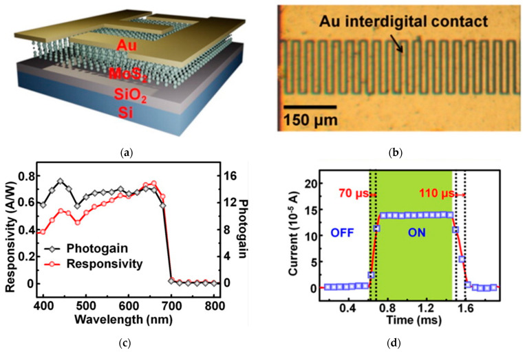
A significantly faster device was produced by Tsai et al. [50], based on a few-layered MoS2 structure obtained through a wet-synthesis approach, and deposited on a Si/SiO2 substrate. The Au electrodes were fabricated by photolithography in an interdigitated fashion (Figure 7) to produce a metal–semiconductor–metal (MSM) Schottky photodiode. The detector showed very fast response to visible light (t_rise = 70 μs, t_fall = 110 μs) and a responsivity of R = 0.57 A/W. The reason for this performance is the good compromise between modest photogain and smart geometry of the device which speeds up the carrier collection. In fact, Au electrodes produced via photolitograpy in an interdigitated fashion with 8μm finger spacing (Figure 7b), play an important role in diminishing the time needed to collect the carriers.
Figure 7.
(a) Scheme of a photoconductor based on MoS2; (b) optical microscope top view of the device, where Au interdigitated contacts are clearly visible; (c) responsivity and photogain for the device over the NUV-IR spectral range; (d) photoswitching time response of the detector. Reprinted with permission from ref. [50]. © 2013, American Chemical Society.
Yore et al. [51] built an array of photodetectors based on MoS2 monolayers through a CVD deposition process, and achieved a response extending towards the ultraviolet spectral region (λ∼400 nm). The devices exhibited a photoresponsivity of about 1 mA/W, with a fast response, t ∼ 0.5 ms. Moreover, the detectors exhibited an extremely low dark current, Id ≤ 10 fA, attributable both to a bipolar Schottky barrier between the MoS2 and the metal contacts, and to a negligible doping of the sample from charge impurities introduced by the substrate through an efficient deposition process.
Lopez-Sanchez et al. [24] developed one of the first phototransistors based on MoS2, obtained through a mechanically exfoliated single layer deposited on a Si/SiO2 substrate. The device showed a responsivity of 880 A/W in the visible range, attributable also to a strong photogain mechanism, which also affected the photoswitching time of the detector, which was about 9 s. They reported a very low value of the dark current, Id = 2 pA, although it was achieved with a strong negative bias of the gate, Vg = −70 V.
A similar device was fabricated by A.R. Klots et al. [29] with faster response, in the order of 1 ms. The light response, although it was lower, reached 50 A/W, due to a photogain contribution of 103 times.
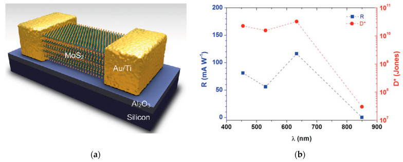
Another low-noise device is described in [23], where a multilayer MoS2 structure obtained through mechanical exfoliation was deposited on Al2O3 (Figure 8). The detector exhibited a responsivity of 0.12 A/W in the visible region, which dropped to very low values for near infrared radiation, attributable to the weak absorption in the IR spectral region. The detector responsivity was also affected by a short carrier lifetime τ, which was determined to be 1.27 ns, limiting the photogain mechanism. Finally, the measured dark currents were as low as 10−11 A. The good response, combined with the very low noise contribution of the system, led to a good detectivity of the device that reached 1011 Jones in the visible region. Moreover, low dark currents were achieved with a low bias of the gate terminal (Vg = −3 V).
Figure 8.
(a) Scheme of a phototransistor based on MoS2. (b) Responsivity and detectivity of the phototransistor over the visible-NIR spectral range. Reprinted with permission from ref. [23]. © 2012, John Wiley and Sons.
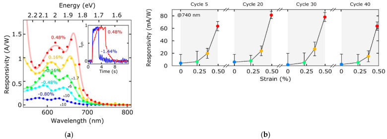
Gant et al. [26] demonstrated a strain tunable photodetector based on a single MoS2 layer structure, obtained by mechanical exfoliation. Their device displayed two to three orders of magnitude of variation in the responsivity when subjected to a strain in the visible range (Figure 9a). The applied strain also caused a variation of the time response from 80 ms to 1.5 s. The variation of both magnitude and time response can be attributed to the creation of trap states in the material during strain. Moreover, the measurements showed a good reproducibility when the device was tested under multiple bending cycles, demonstrating the stability of the material under strain (Figure 9b).
Figure 9.
(a) Responsivity values over the spectral range for a ZnS-MoS2-based device when it is subject to various strains. In the inset the temporal response for different strain applications is shown. (b) Responsivity values against the applied strain increasing the bending cycle number. Reprinted with permission from ref. [26]. © 2019, Elsevier.
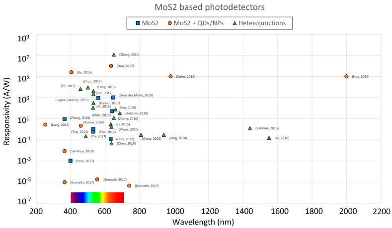
Neat MoS2 photoconductors can reach large values of responsivity when a sufficient voltage bias is applied, attributable to a large photogain contribution and can achieve relatively fast response times if the detector geometry is designed properly (e.g., with interdigitated electrodes). Most of the neat MoS2 photodetectors are characterized in the visible range (400–700 nm) and only very few devices explore the response to the near ultraviolet (NUV) or near infrared (NIR) spectrum (Figure 10). The IR spectrum generally leads to limited response of the material, since the absorption edge of MoS2 lays in the red (≈660 nm) which act as a cutoff for the longer wavelength radiation. On the contrary, the UV response is expected to increase when decreasing the wavelength, as suggested by absorption experiments.
Figure 10.
Responsivity values plotted against the wavelength for various MoS2-based photodetectors.
2.2. MoS2 + QDs Based Photodetectors
To enhance the photodetector response both to NUV and near to mid infrared (NIR-MIR) light spectrum, the MoS2 layer is combined with sensitized centres, namely quantum dots (QDs) or nanoparticles (NPs). Devices belonging to this category generally show high responsivity values also in regions outside the visible spectrum (Figure 10), but are also characterized by slower response, caused by the trap states introduced by the sensitizing centres, which act as impurities.
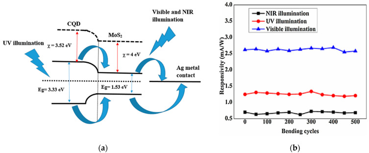
A large area carbon QD-MoS2-based photoconductor was reported by [52] following a hydrothermal method to grow MoS2 on a paper substrate. The device is sensitive in the NUV with a response of 8.4 mA/W to a 365 nm light and an external quantum efficiency (EQE) of 3% for the same wavelength. Carbon QDs possess a higher band-gap compared to MoS2, which is suitable for UV detection (Figure 11a). A response time of 0.57 s was reported for this structure, making the device not applicable for high frequency operations. Due to the intrinsic flexibility of the paper substrate, the device was also tested under multiple bending cycles, revealing no appreciable variation of the light response (Figure 11b), thus demonstrating the possibility to build flexible and wearable electronics. As for other photoconductors, the dark current approached high values (Id = 10−6 A), limiting the sensitivity of the device.
Figure 11.
(a) Electronic band structure alignment for a photodetector based on MoS2 and CQDs. (b) Responsivity values of the device over the bending cycle numbers, demonstrating the stability of the signal over multiple bending cycles. Reprinted with permission from ref. [52]. © 2018, Elsevier.
Similarly, a ZnS-MoS2 structure, deposited on paper, was fabricated by [53] and tested under UV, visible and NIR light (365 nm, 554 nm, 740 nm, respectively). The responsivity of the device in that spectral region remained orders of magnitude lower (10−6–10−5 A/W) than the previously reported values, with response times in the order of 10 s. Although the performances were low, the multiple bending test also gave a successful result in this case.
Much better performance has been obtained with phototransistors sensitized with nanoparticles. These devices require an additional power supply of tens of volts and are based on toxic compounds such as CdSe ([34]), PbS ([32]) and HgTe ([35]), but the dark current can be reduced by several orders of magnitude compared to sensitized photoconductors. Noise suppression makes these detectors highly sensitive, with detectivity values reaching 1013–1015 Jones.
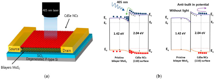
A CdSe sensitized MoS2 phototransistor is reported in [34], based on an exfoliated MoS2 bilayer over a Si/SiO2 substrate (Figure 12). The device showed a responsivity of 2.5 × 10⁵ A/W at 405 nm of incident light, which is the highest light response of a MoS2-based photodetector in the NUV spectral range to the best of our knowledge. Although the responsivity reached very high values, the time response remained as small as 60 ms. The reasons for such performance have to be attributed to the n–n heterojunction formed by the MoS2 bilayer and the CdSe nanocrystals as depicted in Figure 12. In fact, when the UV radiation hits the interface region, the electrons formed in the CdSe nanocrystals are driven to the MoS2 side, while the holes remained confined in the CdSe nanoparticles. When the light was switched off, the electrons accumulated in the valley easily recombined and the n–n barrier prevented the transfer of carriers between the two regions.
Figure 12.
(a) Structure of a phototransistor sensitized with CdSe nanoparticles. (b) Band alignment between MoS2 and CdSe nanoparticles and their carrier representation when light in ON or OFF. Reprinted with permission from ref. [34]. © 2009, Royal Society of Chemistry.
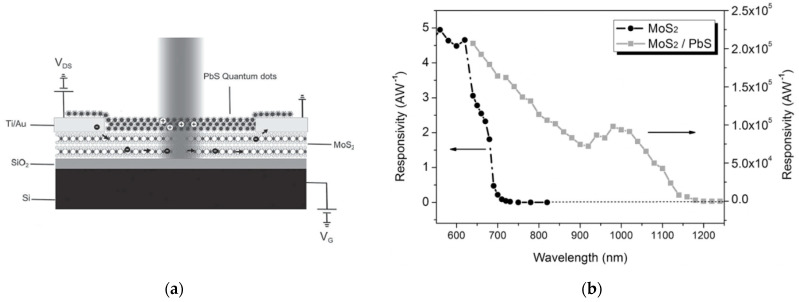
A phototransistor sensitive to the NIR light was reported in [32], composed by a few-layered MoS2 structure obtained through a micromechanical exfoliation, sensitized with a colloidal solution of PbS QDs (Figure 13a). This system, although its speed is limited to a subsecond time response, exhibited a response of 105 A/W to a 980 nm light, and a detectivity of 7 × 10¹⁴ Jones. Additionally, in this case the junction (p-PbS and n-MoS2) plays an important role in determining the response of the device to the incident light. Moreover, the electrons are efficiently transferred from PbS QDs to MoS2, while the holes remain trapped in the PbS side, leading to large photogain and a slow recombination of the carriers.
Figure 13.
(a) Representation of a phototransistor based on MoS2 and PbS quantum dots; (b) Responsivity of the MoS2/Pbs based device compared to the values for the neat MoS2-based device over the visible-NIR spectral range. Reprinted with permission from ref. [32]. © 2014, John Wiley and Sons.
The main limitation of these devices lies in the high gate bias voltage required to achieve such a high detectivity (Vg = −80 V [34], Vg = −100 V [32]), and the intrinsic toxicity of cadmium and lead. The strong gate modulation required can be attributed to the formation of the density of the states within the MoS2 bandgap.
Some efforts have been done to reduce the required gate bias, as in the MoS2 phototransistor sensitized with Hg-Te nanoparticles reported by [35]. The detector showed an extremely high responsivity (105–106 A/W) over a very broad light spectrum, ranging from visible to mid infrared (2000 nm), with a fast response time in the order of milliseconds. Such high responsivity was achieved through a high photogain mechanism, originated from a large hole lifetime (τ = 4 ms) induced by the presence of QDs, which was six orders of magnitude larger than the transit time of the electrons (t = 9 ns). The detectivity measurements showed values of about 1012–1013 Jones over the same spectral range (Figure 14), also due to the low measured value of the dark current (≈10 pA). In this device, a toxic element (Hg) is still present, but the detector was operated at a gate bias of −15 V in depletion regime, which is much lower than in previous devices. The gain in gate modulation can be attributed to the presence of a TiO2 buffer layer that reduces the interaction between MoS2 and HgTe.
Figure 14.
(a) Photodetector based on MoS2 + HgTe; (b,c): responsivity and detectivity values over the vis-IR spectral range, respectively, for the same phototransistor. Reprinted with permission from ref. [35]. © 2017, John Wiley and Sons.
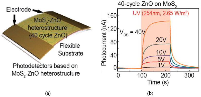
A more recent work [54] has explored the deep UV spectral region reporting a phototransistor based on a thin MoS2 film deposited on a flexible PET substrate, sensitized with ZnO nanoparticles (Figure 15a). The device showed a remarkable responsivity of 2.7 A/W to a 254 nm UV light source. Moreover, the performance was stable under multiple bending cycles. However, the response was slow, reaching tens of seconds, and the bias voltage required to obtain such a high response was set to 40 V (Figure 15b). These results make clear that more efforts have to be undertaken to produce more efficient photodetectors, especially in the deep UV light region, to broaden the possible applications of MoS2 at low photon wavelengths.
Figure 15.
(a) Scheme of a phototransistor based on a MoS2-ZnO structure and developed on a flexible PET substrate; (b) response of the phototransistor to an incident UV (254 nm) light over time. Reprinted with permission from ref. [54]. Copyright 2019, Creative Commons Attribution 3.0 Unported Licence.
2.3. MoS2 + Graphene Based Photodetectors
The possibility to fabricate 2D structures of graphene and the astonishing mobility that it can reach (about 200,000 cm2/(V s) [55]) are some of the primary reasons for the interest in this material. However, its semimetallic behaviour, leading to a zero band gap energy, is a limiting factor in optoelectronic applications [56]. In fact, due to the absence of a forbidden band gap, large currents can be injected into the material. This leads to large dark current values, which limit the sensitivity of a photodetector. Thus, for NUV-vis-NIR application, graphene is often used as contact material [6], together with other finite band gap semiconductors. In this way it is possible to exploit the 2D versatility and high mobility of graphene by combining them with other semiconductor properties.
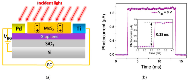
An example of a phototransistor based on MoS2 with graphene is reported by [31]. The device is a lateral photodetector, where few layers of MoS2 were mechanically exfoliated on a sheet of graphene. Two different metal contacts (Pd and Ti) were used to collect the charges (Figure 16).
Figure 16.
(a) Scheme of a phototransistor based on a graphene-MoS2 heterostructure. (b) Time-resolved response of the phototransistor (Vds = 0 V). Reprinted with permission from ref. [31]. © 2015, Elsevier.
The detector exhibited a notable responsivity (R = 3 A/W) with a fast response for a lateral phototransistor (t < 0.13 ms). These results were obtained with zero voltage bias application, due to the asymmetric built-in electric field created at the graphene–electrode interface. In addition, the role of the graphene sheet is also to increase the velocity of the carrier transport to the metal contact, due to its very high mobility. Moreover, the ON/OFF ratio reached a value of 103, while the dark current remained lower than 1 nA.
2.4. MoS2 + TMDs Based Photodetectors
Several studies have reported photodetectors based on heterostructures composed by different TMDs. In these devices, the different electronic band structure forms a built-in electric field at the interface between the materials that speeds up the photogenerated carrier separation. Moreover, the spectral range response of these photodetectors is widened since it involves different semiconductor materials.
Chen et al. [36] proposed a photodiode based on a vertical van der Waals heterojunction between MoS2 and MoTe2, obtained through mechanical exfoliation (Figure 17a). With respect to MoS2, MoTe2 presents a smaller bandgap, which varies from 0.9 to 1.1 eV moving from bulk structure to monolayer. The structure exploits a type II band alignment, which favours the injection of electrons into MoS2 and the injection of holes into MoTe2 (Figure 17b).
Figure 17.
(a) Scheme of a photodetector based on an heterojunction between MoS2 and MoTe2. (b) Type II band alignment between MoTe2 and MoS2; (c) Photoswitching behaviour of the photodetector at V = 0 V. Reprinted with permission from ref. [36]. © 2018, John Wiley and Sons.
The device dispalyed a responsivity of 0.046 A/W to a 637 nm light, with no voltage bias applied. Moreover, the authors measured a response time of about 60 μs, due to the fast separation of carriers that occurs at the junction. In fact, the space charge region near the junction is characterized by a very strong built-in electric field, which becomes stronger as the length of the junction is scaled down, as it happens for vertical herojunctions. The strong interlayer built-in potential provided also a barrier for the dark current, which was measured to be about 3 pA.
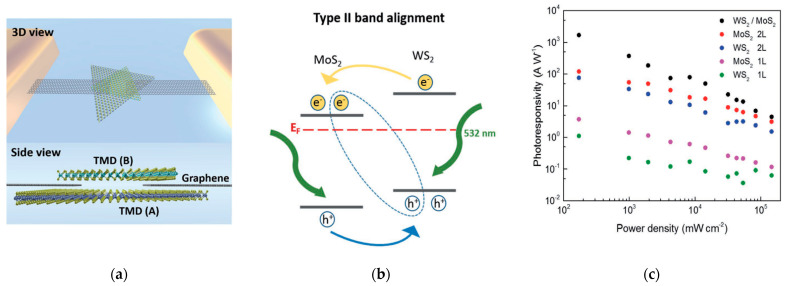
Another vertical heterostructure was reported by Tan et al. [57], who exploited a type II alignment between two monolayers of MoS2 and WS2, both obtained by CVD, with two graphene contacts (Figure 18). The detector exhibited remarkable maximum photoresponsivity (R = 2340 A/W) to 532 nm light. In particular, the photoresponsivity of the heterojunction-based device is at least one order of magnitude higher than the responsivity obtained with the single TMDs (Figure 18c). However, the decay of the response when the light was switched off lasted more than a few seconds. This performance is attributable to an efficient charge transfer at the junction and to trap states for the photogenerated carriers that lead to a photogain of about 3 × 10⁴. In fact, the measured dark current was 10−6 A, several orders of magnitude larger than the previously reported detector [36], due to a much less resistive channel in this case.
Figure 18.
(a) Representation of a MoS2Graphene–WS2 heterostructure; (b) Band alignment at the heterojunction between MoS2 and WS2; (c) photoresponsivity values for different light power input of the WS2-Gr-MoS2 heterostructure (black dots), compared to the responsivity of the single TMDs. Reprinted with permission from ref. [57]. © 2017, John Wiley and Sons.
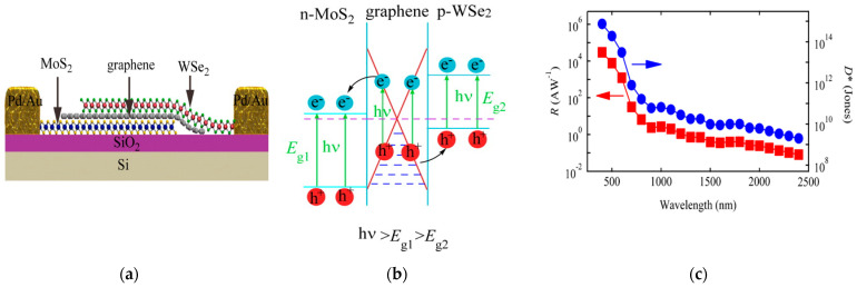
Long et al. [33] reported on a phototransistor based on stacked MoS2–Graphene–WSe2 layers, obtained by mechanical exfoliation (Figure 19a). This device was tested over a broad light spectrum (400–2400 nm). The detector exhibited a responsivity up to 104 A/W in the visible region, which decayed to 300 mA/W approaching the IR region (940 nm), with no gate bias applied (Figure 19c). The calculated specific detectivity was 1015 Jones in the visible region, while decayed to 1011 Jones in the IR region. Finally, the detector showed a time response to visible light of 54 μs, which indicates a fast response of the system, typical in a detector based on a vertical heterojunction.
Figure 19.
(a) Scheme of a phototransistor based on the vertical heterostructure between MoS2, graphene and MoSe2. (b) Band alignment at the heterojunction between TMDs and graphene; (c) responsivity and detectivity values plotted against the incident wavelength for the phototransistor over the vis-IR spectrum. Reprinted with permission from ref. [33]. © 2016, American Chemical Society.
Wi et al. [30] presented a vertical photodiode optimized for UV radiations. The structure is composed of a homojunction between a n-MoS2 layer and a p-MoS2 layer obtained sarting from exfoliation (Figure 20). p-doped MoS2 was obtained by CHF3 plasma treatment, while n-type MoS2 was naturally achieved through the production process. Graphene and gold were then used as contacts. The authors obtained EQE of 80.7% in the UV range (300 nm) and of 51.4 % in the visible range (532 nm).
Figure 20.
(a): Scheme of a photodiode based on a p–n junction of MoS2; (b) energetic band alignment between Graphene/n-MoS2/p-MoS2/Au composing the device; (c): external quantum efficiency (EQE) with respect to the incident wavelength for the device depicted on the left (red curve), compared with the EQE obtained with different plasma doping and different combinations of the electrode materials. Reprinted with permission from ref. [30]. © 2014, AIP Publishing.
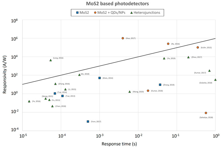
Both the responsivity and the response time have been plotted in Figure 21 for several MoS2-based photodetectors, in order to compare their performance. Since, through the photoconductive gain, the responsivity is directly proportional to the lifetime τr [1,58], a reference line representing the points for which R/τr = 1 A/(W us) has also been included in the graph. As can be observed, only three devices are represented by a point above this line.
Figure 21.
Responsivity values plotted against the response time for various MoS2-based photodetectors. The solid line represents the points for which R/τr = 1 A/ (W μs).
In [33] the separation of the carriers is performed by the built in electric field at the vertical junction between the TMDs, while the transport is performed laterally by graphene, resulting in the best combination for fast carrier transport. Otherwise, devices where TMDs are responsible both for the separation of carriers and for the carrier transport may suffer from a slower response. On the other hand, MoS2-based photodetectors sensitized with QDs or NPs described in [34,35], despite their slower response compared to heterojunction beased structures, reached high performance due to an efficient carrier transfer and a remarkable photogain.
2.5. MoS2 + Perovskites Based Photodetectors
MoS2-based photodetectors often suffer from remarkable noise power density (NPD) and slow responses due to the defects induced on the surface of the MoS2 during the synthesis or from ambient gas absorption (e.g., H2O, O2) [24,59,60]. Passivation is one of the procedures exploited to reduce gas absorption at the MoS2 surface and the introduction of halogens have been reported to be effective on metal calchogenides [61].
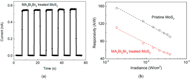
He et al. [25] adopted a layer of methylamine (MA) halide (MA3Bi2Br9) to passivate a MoS2-based photoconductor. Their detector exhibited a high photoresponsivity (R = 112 A/W) and a very fast response (t = 0.3 ms). Moreover, the response of the device achieved a stability over the time, compared to other passivation techniques, as depicted in Figure 22.
Figure 22.
(a) Current measurements over time for a photoconductor based on MoS2 and passivated with MA3Bi2Br9; (b) Responsivity measures against irradiance for pristine MoS2 and MoS2 passivated with MA3Bi2Br9. Reprinted with permission from ref. [25]. © 2018, American Chemical Society.
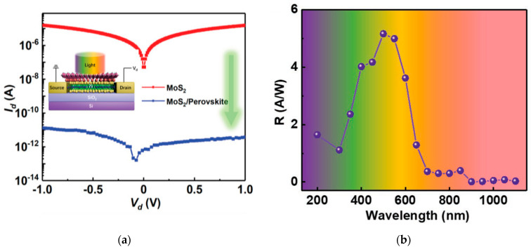
Recently, Wang et al. [28] have introduced a 2D halide perovskite, (C6H5C2H4NH3)2PbI4 ((PEA)2PbI4), over a multilayer MoS2 structure. They achieved a dark current suppression of six orders of magnitude with respect to the neat MoS2 device, reaching 10−11 A (Figure 23a). The reason for this behaviour is found in the electron diffusion from MoS2 to the perovskite: when they are put in contact, it decreases the charge carrier density. The detectivity of the device was improved as well and estimated to be about 1013 Jones. Moreover, the perovskite layer acts as a defect passivator, which resulted in a faster response of the device, that decreased by more than 100-fold with respect to the neat MoS2 case, and showed a response speed of few milliseconds. In this work, the responsivity of the detector was calculated over a broad spectral range that also included the UV spectrum (200–1100 nm) and reached maximum values in the visible range (Figure 23b).
Figure 23.
(a) Dark current comparison between pristine MoS2 and MoS2 passivated with (PEA)2PbI4; (b) Responsivity of the device with respect to the incident wavelength for a UV-vis-NIR spectrum. Reprinted with permission from ref. [28]. © 2020, John Wiley and Sons.
Furthermore the device was found to operate with a zero applied external bias, due to a built-in electric field at the interface between the p-type region of the (PEA)2PbI4 and the n-type region of MoS2, and thus to perform as a photodiode. The response speed measured with zero voltage bias was less than one order of magnitude larger than in the case of the positive bias voltage applied, and reached few tens of milliseconds.
Many other MoS2-based devices have been reported in the literature; the performance of a few other devices ([62,63,64,65,66,67,68,69,70,71,72,73,74,75]), together with the photodetectors we have described so far, are reported in the graphs of Figure 10 and Figure 21.
3. Conclusions
Many photodetectors based on MoS2 have been developed in the last decade, and the most representative have been analyzed in this review. The main characteristics of the devices discussed so far are summarized in Table 1.
Table 1.
MoS2-based photodetector performance. FL = few layers, ML = multilayer, TF = thin film, tr = rise time, td = decay time.
| Photoactive Material | Technology | MoS2 Layers | Wavelength (nm) | Responsivity (A/W) | Response Time (s) | Detectivity (Jones) | Dark Current (A) | Ref. | |
| MoS2 | MoS2 | phototransistor | 1L | 647 | 1000 | 13 | [27] | ||
| MoS2 | MSM photodiode | FL | 532 | 0.57 | tr 7 × 10⁻⁵ td 11 × 10−5 |
1010 | [50] | ||
| MoS2 | MSM photodiode | 1L | ≈400 | 10−3 | 0.5 × 10⁻³ | <10−14 | [51] | ||
| MoS2 | phototransistor | 1L | 561 | 880 | 9 | 2 × 10⁻¹² | [24] | ||
| MoS2 | phototransistor | 1L | 640 | 50 | 10−3 | [29] | |||
| MoS2 | phototransistor | ML | 633 | 0.12 | 1010–1011 | 10−11 | [23] | ||
| MoS2 | photodiode | FL | 365 | 9.3 | tr 3.7 × 10⁻² td 3.9 × 10⁻² |
[62] | |||
| MoS2 | MSM photodiode | 3L | 532 | 1.04 | tr 4 × 10⁻⁵ td 5 × 10⁻⁵ |
[68] | |||
| MoS2 + QDs/NPs | MoS2 + CQD | photoconductor | FL | 365 | 8.4 × 10⁻³ | 0.57 | ≈10−6 | [52] | |
| MoS2 + ZnS | photoconductor | 3L | 554 | 1.79 × 10⁻⁵ | 11 | [53] | |||
| 365 | 9.50 × 10⁻⁶ | 22 | [53] | ||||||
| 780 | 4.52 × 10⁻⁶ | 31 | [53] | ||||||
| MoS2 + CdSe | phototransistor | 2L | 405 | 2.50 × 10⁵ | 0.06 | 1.24 × 10¹⁴ | [34] | ||
| MoS2 + PbS | phototransistor | FL | 980 | 105 | 0.35 | 7 × 10¹⁴ | 2.6 × 10⁻⁷ | [32] | |
| MoS2 + HgTe | phototransistor | FL | 635 | 106 | 10−11 | [35] | |||
| 2000 | 105 | 1012 | [35] | ||||||
| MoS2 + ZnO | phototransistor | TF | 254 | 2.7 | 55 | [54] | |||
| MoS2 Heterostructures | MoS2 + Gr | phototransistor | FL | 632.8 | 3 | <1.3 × 10⁻⁴ | 9 × 10⁻¹⁰ | [31] | |
| MoS2 + MoTe2 | photodiode | FL | 637 | 4.60 × 10⁻² | 6 × 10⁻⁵ | 1.06 × 10⁸ | 3 × 10⁻¹² | [36] | |
| MoS2 + WS2 | phototransistor | 1L | 532 | 2340 | 4.1 × 10¹¹ | 10−6 | [57] | ||
| MoS2 + Gr + WSe2 | phototransistor | 1L/FL | 532 | 4250 | 5.4 × 10⁻⁵ | 1015 | [33] | ||
| 940 | 0.3 | 1011 | [33] | ||||||
| MoS2 + MA | photoconductor | 15L | 530 | 112 | 3 × 10⁻⁴ | 3.8 × 10¹² | 4 × 10⁻⁹ | [25] | |
| MoS2 + (PEA)2PbI4 | photoconductor | ML | 637 | 1.68 | tr 6 × 10⁻³
tr 4 × 10⁻³ |
1.06 × 10¹³ | 10−11 | [28] |
Photoconductors based on MoS2 are the simplest structure of photodetectors and they are able to reach very high responsivity values. On the contrary they generally suffer from a slow response, due to absence of a built-in electric field, and from high dark currents that limit the sensitivity of the device. Phototransistors based on MoS2 represent a more mature architecture for detecting light, due to the possibility to suppress dark current signals with an appropriate voltage bias applied at the gate terminal. Although so far very few works report the response of the MoS2 device to the UV and IR spectral regions, they clearly show that there is room for improvement if this material is coupled with other TMDs, graphene or quantum dots. These properties, combined with the thin structures of MoS2 that can be fabricated, allow us to build wide-spectrum bendable detectors.
In this direction, devices based on MoS2 sensitized with NPs or QDs are able to boost the response of the detectors both in the NIR-MIR and in the NUV spectrum, and are often characterized by very high responsivity values. However, the defects induced on MoS2 in consequence of the introduction of sensitizing centres, cause large dark current and slow response.
Heterostructures between MoS2 ond other materials (e.g., TMDs and graphene) are able to extend the response to a wider spectral range as well, and have been demonstrated to be suitable for the fabrication of fast photodiodes, exploiting the built-in electric field that forms at the heterointerface. Moreover, these devices are able to work also at zero-bias mode, without requiring an external power supply. The main drawback for photodiodes is instead represented by the lower responsivity that they can reach, due to the absence of the photogain mechanism. In heterostructures based on MoS2, the second material can act as a passivation layer, preventing the adsorption of oxygen and water molecules on the MoS2 surface. In this way halide perovskites have been demonstrated to be a good solution, leading to a stable and faster response of the devices.
Author Contributions
Conceptualization, A.T., S.D. and L.P.; Methodology, A.T. and L.P.; Validation, A.T., S.D., A.Q. and L.P.; Resources, S.D., L.P. and A.Q.; Data Curation, A.T.; Writing—Original Draft Preparation, A.T.; Writing—Review & Editing, A.T., S.D., L.P. and A.Q.; Visualization, A.T.; Supervision, S.D., L.P. and A.Q.; Project Administration, L.P.; Funding Acquisition, S.D., L.P. and A.Q. All authors have read and agreed to the published version of the manuscript.
Funding
This work was performed in the frame of the program Departments of Excellence 2018-2022 (DII-UNITN)—Italian Ministry of University and Research (MIUR).
Institutional Review Board Statement
Not applicable.
Informed Consent Statement
Not applicable.
Data Availability Statement
Data available on request.
Conflicts of Interest
The authors declare no conflict of interest.
Footnotes
Publisher’s Note: MDPI stays neutral with regard to jurisdictional claims in published maps and institutional affiliations.
References
- 1.Huo N., Konstantatos G. Recent progress and future prospects of 2D-based photodetectors. Adv. Mater. 2018;30:1801164. doi: 10.1002/adma.201801164. [DOI] [PubMed] [Google Scholar]
- 2.Mueller T., Xia F., Avouris P. Graphene photodetectors for high-speed optical communications. Nat. Photonics. 2010;4:297–301. doi: 10.1038/nphoton.2010.40. [DOI] [Google Scholar]
- 3.Radisavljevic B., Radenovic A., Brivio J., Giacometti V., Kis A. Single-layer MoS2 transistors. Nat. Nanotechnol. 2011;6:147–150. doi: 10.1038/nnano.2010.279. [DOI] [PubMed] [Google Scholar]
- 4.Mak K.F., Lee C., Hone J., Shan J., Heinz T.F. Atomically thin MoS2: A new direct-gap semiconductor. Phys. Rev. Lett. 2010;105:136805. doi: 10.1103/PhysRevLett.105.136805. [DOI] [PubMed] [Google Scholar]
- 5.Bernardi M., Palummo M., Grossman J.C. Extraordinary sunlight absorption and one nanometer thick photovoltaics using two-dimensional monolayer materials. Nano Lett. 2013;13:3664–3670. doi: 10.1021/nl401544y. [DOI] [PubMed] [Google Scholar]
- 6.Li X., Tao L., Chen Z., Fang H., Li X., Wang X., Xu J.B., Zhu H. Graphene and related two-dimensional materials: Structure-property relationships for electronics and optoelectronics. Appl. Phys. Rev. 2017;4:021306. doi: 10.1063/1.4983646. [DOI] [Google Scholar]
- 7.Sandoval S.J., Yang D., Frindt R.F., Irwin J.C. Raman study and lattice dynamics of single molecular layers of MoS2. Phys. Rev. B. 1991;44:3955–3962. doi: 10.1103/PhysRevB.44.3955. [DOI] [PubMed] [Google Scholar]
- 8.Voiry D., Goswami A., Kappera R., Silva C., Kaplan D., Fujita T., Chen M., Asefa T., Chhowalla M. Covalent functionalization of monolayered transition metal dichalcogenides by phase engineering. Nat. Chem. 2015;7:45–49. doi: 10.1038/nchem.2108. [DOI] [PubMed] [Google Scholar]
- 9.Kang Y., Najmaei S., Liu Z., Bao Y., Wang Y., Zhu X., Halas N.J., Nordlander P., Ajayan P.M., Lou J., et al. Plasmonic Hot Electron Induced Structural Phase Transition in a MoS2 Monolayer. Adv. Mater. 2014;26:6467–6471. doi: 10.1002/adma.201401802. [DOI] [PubMed] [Google Scholar]
- 10.Katagiri Y., Nakamura T., Ishii A., Ohata C., Hasegawa M., Katsumoto S., Cusati T., Fortunelli A., Iannaccone G., Fiori G., et al. Gate-tunable atomically thin lateral MoS2 Schottky junction patterned by electron beam. Nano Lett. 2016;16:3788–3794. doi: 10.1021/acs.nanolett.6b01186. [DOI] [PubMed] [Google Scholar]
- 11.Li T., Galli G. Electronic Properties of MoS2 Nanoparticles. J. Phys. Chem. C. 2007;111:16192–16196. doi: 10.1021/jp075424v. [DOI] [Google Scholar]
- 12.Lebègue S., Eriksson O. Electronic structure of two-dimensional crystals from ab initio theory. Phys. Rev. B Condens. Matter Mater. Phys. 2009;79 doi: 10.1103/PhysRevB.79.115409. [DOI] [Google Scholar]
- 13.Cheiwchanchamnangij T., Lambrecht W.R.L. Quasiparticle band structure calculation of monolayer, bilayer, and bulk MoS2. Phys. Rev. B Condens. Matter Mater. Phys. 2012;85 doi: 10.1103/PhysRevB.85.205302. [DOI] [Google Scholar]
- 14.Kam K.K., Parkinson B.A. Detailed photocurrent spectroscopy of the semiconducting group VIB transition metal dichalcogenides. J. Phys. Chem. 1982;86:463–467. doi: 10.1021/j100393a010. [DOI] [Google Scholar]
- 15.Splendiani A., Sun L., Zhang Y., Li T., Kim J., Chim C.Y., Galli G., Wang F. Emerging photoluminescence in monolayer MoS2. Nano Lett. 2010;10:1271–1275. doi: 10.1021/nl903868w. [DOI] [PubMed] [Google Scholar]
- 16.Xiao D., Liu G.B., Feng W., Xu X., Yao W. Coupled spin and valley physics in monolayers of MoS2 and other group-VI dichalcogenides. Phys. Rev. Lett. 2012;108 doi: 10.1103/PhysRevLett.108.196802. [DOI] [PubMed] [Google Scholar]
- 17.Zeng H., Dai J., Yao W., Xiao D., Cui X. Valley polarization in MoS2 monolayers by optical pumping. Nat. Nanotechnol. 2012;7 doi: 10.1038/nnano.2012.95. [DOI] [PubMed] [Google Scholar]
- 18.Schaibley J.R., Yu H., Clark G., Rivera P., Ross J.S., Seyler K.L., Yao W., Xu X. Valleytronics in 2D materials. Nat. Rev. Mater. 2016;1:16055. doi: 10.1038/natrevmats.2016.55. [DOI] [Google Scholar]
- 19.Liu Y., Gao Y., Zhang S., He J., Yu J., Liu Z. Valleytronics in transition metal dichalcogenides materials. Nano Res. 2019;12 doi: 10.1007/s12274-019-2497-2. [DOI] [Google Scholar]
- 20.Dhakal K.P., Duong D.L., Lee J., Nam H., Kim M., Kan M., Lee Y.H., Kim J. Confocal absorption spectral imaging of MoS2: Optical transitions depending on the atomic thickness of intrinsic and chemically doped MoS2. Nanoscale. 2014;6 doi: 10.1039/C4NR03703K. [DOI] [PubMed] [Google Scholar]
- 21.Kwak J.Y. Absorption coefficient estimation of thin MoS2 film using attenuation of silicon substrate Raman signal. Results Phys. 2019;13:102202. doi: 10.1016/j.rinp.2019.102202. [DOI] [Google Scholar]
- 22.Novoselov K.S., Jiang D., Schedin F., Booth T.J., Khotkevich V.V., Morozov S.V., Geim A.K. Two-dimensional atomic crystals. Proc. Natl. Acad. Sci. USA. 2005;102 doi: 10.1073/pnas.0502848102. [DOI] [PMC free article] [PubMed] [Google Scholar]
- 23.Choi W., Cho M.Y., Konar A., Lee J.H., Cha G.B., Hong S.C., Kim S., Kim J., Jena D., Joo J., et al. High-detectivity multilayer MoS2 phototransistors with spectral response from ultraviolet to infrared. Adv. Mater. 2012;24:5832–5836. doi: 10.1002/adma.201201909. [DOI] [PubMed] [Google Scholar]
- 24.Lopez-Sanchez O., Lembke D., Kayci M., Radenovic A., Kis A. Ultrasensitive photodetectors based on monolayer MoS2. Nat. Nanotechnol. 2013;8:497–501. doi: 10.1038/nnano.2013.100. [DOI] [PubMed] [Google Scholar]
- 25.He J., Yang Y., He Y., Ge C., Zhao Y., Gao L., Tang J. Low Noise and Fast Photoresponse of Few-Layered MoS2 Passivated by MA3Bi2Br9. ACS Photonics. 2018;5:1877–1884. doi: 10.1021/acsphotonics.8b00129. [DOI] [Google Scholar]
- 26.Gant P., Huang P., de Lara D.P., Guo D., Frisenda R., Castellanos-Gomez A. A strain tunable single-layer MoS2 photodetector. Mater. Today. 2019;27:8–13. doi: 10.1016/j.mattod.2019.04.019. [DOI] [Google Scholar]
- 27.Gonzalez Marin J.F., Unuchek D., Watanabe K., Taniguchi T., Kis A. MoS2 photodetectors integrated with photonic circuits. NPJ 2D Mater. Appl. 2019;3 doi: 10.1038/s41699-019-0096-4. [DOI] [Google Scholar]
- 28.Wang H., Wang X., Chen Y., Zhang S., Jiang W., Zhang X., Qin J., Wang J., Li X., Pan Y., et al. Extremely Low Dark Current MoS2 Photodetector via 2D Halide Perovskite as the Electron Reservoir. Adv. Opt. Mater. 2020;8:1901402. doi: 10.1002/adom.201901402. [DOI] [Google Scholar]
- 29.Klots A.R., Newaz A.K.M., Wang B., Prasai D., Krzyzanowska H., Lin J., Caudel D., Ghimire N.J., Yan J., Ivanov B.L., et al. Probing excitonic states in suspended two-dimensional semiconductors by photocurrent spectroscopy. Sci. Rep. 2014;4:6608. doi: 10.1038/srep06608. [DOI] [PMC free article] [PubMed] [Google Scholar]
- 30.Wi S., Chen M., Nam H., Liu A.C., Meyhofer E., Liang X. High blue-near ultraviolet photodiode response of vertically stacked graphene-MoS2-metal heterostructures. Appl. Phys. Lett. 2014;104:232103. doi: 10.1063/1.4882417. [DOI] [Google Scholar]
- 31.Li X., Wu J., Mao N., Zhang J., Lei Z., Liu Z., Xu H. A self-powered graphene-MoS2 hybrid phototransistor with fast response rate and high on-off ratio. Carbon N. Y. 2015;92:126–132. doi: 10.1016/j.carbon.2015.03.064. [DOI] [Google Scholar]
- 32.Kufer D., Nikitskiy I., Lasanta T., Navickaite G., Koppens F.H.L., Konstantatos G. Hybrid 2D-0D MoS2-PbS quantum dot photodetectors. Adv. Mater. 2015;27:176–180. doi: 10.1002/adma.201402471. [DOI] [PubMed] [Google Scholar]
- 33.Long M., Liu E., Wang P., Gao A., Xia H., Luo W., Wang B., Zeng J., Fu Y., Xu K., et al. Broadband Photovoltaic Detectors Based on an Atomically Thin Heterostructure. Nano Lett. 2016;16:2254–2259. doi: 10.1021/acs.nanolett.5b04538. [DOI] [PubMed] [Google Scholar]
- 34.Ra H.S., Kwak D.H., Lee J.S. A hybrid MoS2 nanosheet-CdSe nanocrystal phototransistor with a fast photoresponse. Nanoscale. 2016;8:17223–17230. doi: 10.1039/C6NR05393A. [DOI] [PubMed] [Google Scholar]
- 35.Huo N., Gupta S., Konstantatos G. MoS2–HgTe Quantum Dot Hybrid Photodetectors beyond 2 µm. Adv. Mater. 2017;29:1606576. doi: 10.1002/adma.201606576. [DOI] [PubMed] [Google Scholar]
- 36.Chen Y., Wang X., Wu G., Wang Z., Fang H., Lin T., Sun S., Shen H., Hu W., Wang J., et al. High-Performance Photovoltaic Detector Based on MoTe2/MoS2 Van der Waals Heterostructure. Small. 2018;14:1703293. doi: 10.1002/smll.201703293. [DOI] [PubMed] [Google Scholar]
- 37.Magda G.Z., Petõ J., Dobrik G., Hwang C., Biró L.P., Tapasztó L. Exfoliation of large-area transition metal chalcogenide single layers. Sci. Rep. 2015;5:14714. doi: 10.1038/srep14714. [DOI] [PMC free article] [PubMed] [Google Scholar]
- 38.Sun J., Li X., Guo W., Zhao M., Fan X., Dong Y., Xu C., Deng J., Fu Y. Synthesis methods of two-dimensional MoS2: A brief review. Crystals. 2017;7:198. doi: 10.3390/cryst7070198. [DOI] [Google Scholar]
- 39.Ahn C., Lee J., Kim H.U., Bark H., Jeon M., Ryu G.H., Lee Z., Yeom G.Y., Kim K., Jung J., et al. Low-Temperature Synthesis of Large-Scale Molybdenum Disulfide Thin Films Directly on a Plastic Substrate Using Plasma-Enhanced Chemical Vapor Deposition. Adv. Mater. 2015;27:5223–5229. doi: 10.1002/adma.201501678. [DOI] [PubMed] [Google Scholar]
- 40.Zhou X., Xu B., Lin Z., Shu D., Ma L. Hydrothermal synthesis of flower-like MoS2nanospheres for electrochemical supercapacitors. J. Nanosci. Nanotechnol. 2014;14:7250–7254. doi: 10.1166/jnn.2014.8929. [DOI] [PubMed] [Google Scholar]
- 41.Feng X., Tang Q., Zhou J., Fang J., Ding P., Sun L., Shi L. Novel mixed-solvothermal synthesis of MoS2 nanosheets with controllable morphologies. Cryst. Res. Technol. 2013;48:363–368. doi: 10.1002/crat.201300003. [DOI] [Google Scholar]
- 42.Nardi M.V., Timpel M., Ligorio G., Zorn Morales N., Chiappini A., Toccoli T., Verucchi R., Ceccato R., Pasquali L., List-Kratochvil E.J.W., et al. Versatile and Scalable Strategy to Grow Sol-Gel Derived 2H-MoS2 Thin Films with Superior Electronic Properties: A Memristive Case. ACS Appl. Mater. Interfaces. 2018;10:34392–34400. doi: 10.1021/acsami.8b12596. [DOI] [PubMed] [Google Scholar]
- 43.Suh J., Park T.E., Lin D.Y., Fu D., Park J., Jung H.J., Chen Y., Ko C., Jang C., Sun Y., et al. Doping against the native propensity of MoS2: Degenerate hole doping by cation substitution. Nano Lett. 2014;14 doi: 10.1021/nl503251h. [DOI] [PubMed] [Google Scholar]
- 44.Li M., Yao J., Wu X., Zhang S., Xing B., Niu X., Yan X., Yu Y., Liu Y., Wang Y. P-type Doping in Large-Area Monolayer MoS2 by Chemical Vapor Deposition. ACS Appl. Mater. Interfaces. 2020;12:6276–6282. doi: 10.1021/acsami.9b19864. [DOI] [PubMed] [Google Scholar]
- 45.Kim E., Ko C., Kim K., Chen Y., Suh J., Ryu S.G., Wu K., Meng X., Suslu A., Tongay S., et al. Site Selective Doping of Ultrathin Metal Dichalcogenides by Laser-Assisted Reaction. Adv. Mater. 2016;28:341–346. doi: 10.1002/adma.201503945. [DOI] [PubMed] [Google Scholar]
- 46.Zhang K., Feng S., Wang J., Azcatl A., Lu N., Addou R., Wang N., Zhou C., Lerach J., Bojan V., et al. Erratum: Manganese Doping of Monolayer MoS2: The Substrate Is Critical (Nano Letters 2015, 15:10 (6586-6591) 10.1021/acs.nanolett.5b02315) Nano Lett. 2016;16:2125. doi: 10.1021/acs.nanolett.6b00760. [DOI] [PubMed] [Google Scholar]
- 47.Chen M., Nam H., Wi S., Ji L., Ren X., Bian L., Lu S., Liang X. Stable few-layer MoS2 rectifying diodes formed by plasma-assisted doping. Appl. Phys. Lett. 2013;103:142110. doi: 10.1063/1.4824205. [DOI] [Google Scholar]
- 48.Mouri S., Miyauchi Y., Matsuda K. Tunable photoluminescence of monolayer MoS2 via chemical doping. Nano Lett. 2013;13:5944–5948. doi: 10.1021/nl403036h. [DOI] [PubMed] [Google Scholar]
- 49.Nakotte T., Luo H., Pietryga J. PbE (E = S, Se) colloidal quantum dot-layered 2D material hybrid photodetectors. Nanomaterials. 2020;10:172. doi: 10.3390/nano10010172. [DOI] [PMC free article] [PubMed] [Google Scholar]
- 50.Tsai D.S., Liu K.K., Lien D.H., Tsai M.L., Kang C.F., Lin C.A., Li L.J., He J.H. Few-layer MoS2 with high broadband photogain and fast optical switching for use in harsh environments. ACS Nano. 2013;7:3905–3911. doi: 10.1021/nn305301b. [DOI] [PubMed] [Google Scholar]
- 51.AYore E., Smithe K.K.H., Jha S., Ray K., Pop E., Newaz A.K.M. Large array fabrication of high performance monolayer MoS2 photodetectors. Appl. Phys. Lett. 2017;111:043110. doi: 10.1063/1.4995984. [DOI] [Google Scholar]
- 52.Sahatiya P., Jones S.S., Badhulika S. 2D MoS2–carbon quantum dot hybrid based large area, flexible UV–vis–NIR photodetector on paper substrate. Appl. Mater. Today. 2018;10:106–114. doi: 10.1016/j.apmt.2017.12.013. [DOI] [Google Scholar]
- 53.Gomathi P.T., Sahatiya P., Badhulika S. Large-Area, Flexible Broadband Photodetector Based on ZnS–MoS2 Hybrid on Paper Substrate. Adv. Funct. Mater. 2017;27:1701611. doi: 10.1002/adfm.201701611. [DOI] [Google Scholar]
- 54.Kang M.A., Kim S., Jeon I.S., Lim Y.R., Park C.Y., Song W., Lee S.S., Lim J., An K.S., Myung S. Highly efficient and flexible photodetector based on MoS2-ZnO heterostructures. RSC Adv. 2019;9:19707–19711. doi: 10.1039/C9RA00578A. [DOI] [PMC free article] [PubMed] [Google Scholar]
- 55.Bolotin K.I., Sikes K.J., Jiang Z., Klima M., Fudenberg G., Hone J., Kim P., Stormer H.L. Ultrahigh electron mobility in suspended graphene. Solid State Commun. 2008;146:351–355. doi: 10.1016/j.ssc.2008.02.024. [DOI] [Google Scholar]
- 56.Mak K.F., Shan J. Photonics and optoelectronics of 2D semiconductor transition metal dichalcogenides. Nat. Photonics. 2016;10:216–226. doi: 10.1038/nphoton.2015.282. [DOI] [Google Scholar]
- 57.Tan H., Xu W., Sheng Y., Lau C.S., Fan Y., Chen Q., Tweedie M., Wang X., Zhou Y., Warner J.H. Lateral Graphene-Contacted Vertically Stacked WS2/MoS2 Hybrid Photodetectors with Large Gain. Adv. Mater. 2017;29:1702917. doi: 10.1002/adma.201702917. [DOI] [PubMed] [Google Scholar]
- 58.Zheng K., Luo L.B., Zhang T.F., Liu Y.H., Yu Y.Q., Lu R., Qiu H.L., Li Z.J., Huang J.C.A. Optoelectronic characteristics of a near infrared light photodetector based on a topological insulator Sb2Te3 film. J. Mater. Chem. C. 2015;3:9154–9160. doi: 10.1039/C5TC01772F. [DOI] [Google Scholar]
- 59.Furchi M.M., Polyushkin D.K., Pospischil A., Mueller T. Mechanisms of photoconductivity in atomically thin MoS2. Nano Lett. 2014;14:6165–6170. doi: 10.1021/nl502339q. [DOI] [PubMed] [Google Scholar]
- 60.Pak J., Min M., Cho K., Lien D.H., Ahn G.H., Jang J., Yoo D., Chung S., Javey A., Lee T. Improved photoswitching response times of MoS2 field-effect transistors by stacking p -type copper phthalocyanine layer. Appl. Phys. Lett. 2016;109:183502. doi: 10.1063/1.4966668. [DOI] [Google Scholar]
- 61.Tang J., Kemp K.W., Hoogland S., Jeong K.S., Liu H., Levina L., Furukawa M., Wang X., Debnath R., Cha D., et al. Colloidal-quantum-dot photovoltaics using atomic-ligand passivation. Nat. Mater. 2011;10:765–771. doi: 10.1038/nmat3118. [DOI] [PubMed] [Google Scholar]
- 62.Zhang X.M., Tseng S.H., Lu M.Y. Large-area ultraviolet photodetectors based on p-type multilayer MoS2 enabled by plasma doping. Appl. Sci. 2019;9:1110. doi: 10.3390/app9061110. [DOI] [Google Scholar]
- 63.Kumar R., Goel N., Raliya R., Biswas P., Kumar M. High-performance photodetector based on hybrid of MoS2 and reduced graphene oxide. Nanotechnology. 2018;29:404001. doi: 10.1088/1361-6528/aad2f6. [DOI] [PubMed] [Google Scholar]
- 64.Solanke S., Rathakanthiwar S., Kalra A., Rangarajan M., Raghavan S., Nath D.N. Multi-layer MoS2/GaN UV-Visible photodetector with observation of MoS2band edge in spectral responsivity. arXiv. 20181803.11012 [Google Scholar]
- 65.Kumar R., Sharma A., Kaur M., Husale S. Pt-Nanostrip-Enabled Plasmonically Enhanced Broad Spectral Photodetection in Bilayer MoS2. Adv. Opt. Mater. 2017;5:1700009. doi: 10.1002/adom.201700009. [DOI] [Google Scholar]
- 66.Zhou X., Zhou N., Li C., Song H., Zhang Q., Hu X., Gan L., Li H., Lü J., Luo J., et al. Vertical heterostructures based on SnSe2/MoS2 for high performance photodetectors. 2D Mater. 2017;4:025048. doi: 10.1088/2053-1583/aa6422. [DOI] [Google Scholar]
- 67.Yu W.J., Liu Y., Zhou H., Yin A., Li Z., Huang Y., Duan X. Highly efficient gate-tunable photocurrent generation in vertical heterostructures of layered materials. Nat. Nanotechnol. 2013;8:952–958. doi: 10.1038/nnano.2013.219. [DOI] [PMC free article] [PubMed] [Google Scholar]
- 68.Tsai D.S., Lien D.H., Tsai M.L., Su S.H., Chen K.M., Ke J.J., Yu Y.C., Li L.J., He J.H. Trilayered MoS2 metal-Semiconductor-metal photodetectors: Photogain and radiation resistance. IEEE J. Sel. Top. Quantum Electron. 2014;20:3800206. doi: 10.1109/JSTQE.2013.2268383. [DOI] [Google Scholar]
- 69.Zhang W., Chuu C.P., Huang J.K., Chen C.H., Tsai M.L., Chang Y.H., Liang C.T., Chen Y.Z., Chueh Y.L., He J.H., et al. Ultrahigh-Gain Photodetectors Based on Atomically Thin Graphene-MoS2 Heterostructures. Sci. Rep. 2015;4:3826. doi: 10.1038/srep03826. [DOI] [PMC free article] [PubMed] [Google Scholar]
- 70.Vabbina P., Choudhary N., Chowdhury A.A., Sinha R., Karabiyik M., Das S., Choi W., Pala N. Highly Sensitive Wide Bandwidth Photodetector Based on Internal Photoemission in CVD Grown p-Type MoS2/Graphene Schottky Junction. ACS Appl. Mater. Interfaces. 2015;7:15206–15213. doi: 10.1021/acsami.5b00887. [DOI] [PubMed] [Google Scholar]
- 71.Ye K., Liu L., Liu Y., Nie A., Zhai K., Xiang J., Wang B., Wen F., Mu C., Zhao Z., et al. Lateral Bilayer MoS2–WS2 Heterostructure Photodetectors with High Responsivity and Detectivity. Adv. Opt. Mater. 2019;7:1900815. doi: 10.1002/adom.201900815. [DOI] [Google Scholar]
- 72.Shin G.H., Park J., Lee K.J., Lee G.B., Jeon H.B., Choi Y.K., Yu K., Choi S.Y. Si-MoS2 vertical heterojunction for a photodetector with high responsivity and low noise equivalent power. ACS Appl. Mater. Interfaces. 2019;11:7626–7634. doi: 10.1021/acsami.8b21629. [DOI] [PubMed] [Google Scholar]
- 73.Wang L., Jie J., Shao Z., Zhang Q., Zhang X., Wang Y., Sun Z., Lee S.T. MoS2/Si heterojunction with vertically standing layered structure for ultrafast, high-detectivity, self-driven visible-near infrared photodetectors. Adv. Funct. Mater. 2015;25:2910–2919. doi: 10.1002/adfm.201500216. [DOI] [Google Scholar]
- 74.Zhang Y., Yu Y., Mi L., Wang H., Zhu Z., Wu Q., Zhang Y., Jiang Y. In Situ Fabrication of Vertical Multilayered MoS2/Si Homotype Heterojunction for High-Speed Visible-Near-Infrared Photodetectors. Small. 2016;12:1062–1071. doi: 10.1002/smll.201502923. [DOI] [PubMed] [Google Scholar]
- 75.Ye L., Li H., Chen Z., Xu J. Near-Infrared Photodetector Based on MoS2/Black Phosphorus Heterojunction. ACS Photonics. 2016;3:692–699. doi: 10.1021/acsphotonics.6b00079. [DOI] [Google Scholar]
Associated Data
This section collects any data citations, data availability statements, or supplementary materials included in this article.
Data Availability Statement
Data available on request.


