Abstract
Monolayer MoS2 is a promising semiconductor to overcome the physical dimension limits of microelectronic devices. Understanding the thermochemical stability of MoS2 is essential since these devices generate heat and are susceptible to oxidative environments. Herein, the promoting effect of molybdenum oxides (MoOx) particles on the thermal oxidation of MoS2 monolayers is shown by employing operando X‐ray absorption spectroscopy, ex situ scanning electron microscopy and X‐ray photoelectron spectroscopy. The study demonstrates that chemical vapor deposition‐grown MoS2 monolayers contain intrinsic MoOx and are quickly oxidized at 100 °C (3 vol% O2/He), in contrast to previously reported oxidation thresholds (e.g., 250 °C, t ≤ 1 h in the air). Otherwise, removing MoOx increases the thermal oxidation onset temperature of monolayer MoS2 to 300 °C. These results indicate that MoOx promote oxidation. An oxide‐free lattice is critical to the long‐term stability of monolayer MoS2 in state‐of‐the‐art 2D electronic, optical, and catalytic applications.
Keywords: 2D materials, monolayer molybdenum disulfide, operando oxidation, thermochemistry
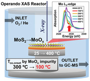
Operando X‐ray absorption spectroscopy elucidates molybdenum oxide (MoOx) impurities’ effect on the thermochemical stability of monolayer MoS2. The thermal oxidation onset of as‐grown monolayer MoS2 is as low as 100 °C with MoOx present, overestimated by >150 °C in the literature (T ≥ 250 °C, t ≤ 1 h). Removal of MoOx increases the oxidation onset temperature to 300 °C.
Monolayer molybdenum disulfide (MoS2) is an atomically thin semiconductor with a sub‐nanometer thickness (6.5–8 Å),[ 1 , 2 ] high electron mobility (≈200 cm2 V−1 s−1),[ 1 ] a direct band gap (1.8–2.2 eV),[ 1 , 3 ] and high current on/off ratio (>108).[ 1 ] MoS2 monolayers[ 4 ] can potentially be used for flexible electronics and push the physical dimension limits of microelectronics.[ 4 , 5 , 6 ] Towards these visions, great progress has been made on the synthesis of wafer‐scale polycrystalline MoS2 monolayers,[ 7 ] and large‐domain (≈500 µm) single‐crystalline MoS2 monolayers by chemical vapor deposition (CVD),[ 2 ] and the wafer‐scale transfer and stacking of monolayer MoS2 for heterogeneous integrations.[ 8 , 9 ] In practice, microelectronics dissipate energy through Joule heating,[ 10 ] and MoS2 monolayer transistors reach average operating temperatures of >150 °C with local hot spots of >250 °C.[ 10 , 11 ] Therefore, investigating the thermochemical stability of MoS2 above room temperature (RT) and under the device working temperature range is important.
Past studies on the thermal oxidation of MoS2 reported that the oxidation process is fast when the temperature is above ≈250 °C (e.g., 250 °C in the air for 1 h,[ 12 ] 360 °C in the air for 5 min,[ 13 ] and 380 °C in the air for 10 min; Table S1, Supporting Information).[ 10 ] These findings were supported by ex situ observations of pits and crack formation, and identification of molybdenum oxides via atomic force microscopy (AFM),[ 12 , 13 , 14 , 15 , 16 ] scanning electron microscopy (SEM),[ 13 , 15 , 17 ] transmission electron microscopy (TEM),[ 17 ] X‐ray photoelectron spectroscopy (XPS),[ 12 , 16 , 17 ] nanomechanical means,[ 16 ] and Raman spectroscopy.[ 14 ] Such ex situ characterization methods, although very informative, may not detect subtle morphological and chemical compositional changes brought on by MoS2 oxidation. Importantly, the previous thermal oxidation studies assumed chemically pure MoS2 monolayers. However, many reported as‐grown monolayers frequently showed an XPS peak indicative of Mo6+ 3d3/2 from MoO3 at ≈236.5 eV.[ 4 , 18 , 19 ] Even though molybdenum oxides (MoOx) are known to activate and transfer oxygen,[ 20 , 21 ] are defective,[ 22 , 23 ] and oxophilic,[ 24 ] their effect on the oxidation of MoS2 has not been systematically investigated.
Herein, we characterize the thermal oxidation of MoS2 monolayers with and without MoOx at atmospheric pressure in the temperature range of 25–400 °C using a novel ultrasensitive operando X‐ray absorption spectroscopy (XAS). We report the first XAS measurement of an atomically thin monolayer MoS2 under dynamic environments (i.e., temperature ramping up to 400 °C, 3 vol% O2/He, 101.3 kPa, with X‐rays in the energy range of 2–3 keV) and it is complemented by ex situ XAS, SEM, and XPS. Such unique measurements of monolayer species were performed using our newly designed operando XAS reactor that enables an ultrasensitive electron yield (EY) detection mode under actual reactive environments;[ 25 , 26 , 27 , 28 , 29 ] different to conventional fluorescence and transmission modes (see Table S2, Supporting Information, for details). Our study shows that as‐grown MoS2 monolayers via CVD contain trace amounts of oxygenated Mo4+ and Mo6+. Without removing the MoOx, the oxidation of MoS2 monolayer was activated starting as low as 100 °C even in a diluted oxidative atmosphere at ambient pressure (3 vol% O2 in inert gas). After removing MoOx, the oxidation onset temperature of MoS2 monolayers is increased to 300 °C. Our work shows that an oxide‐free and high‐purity monolayer MoS2 is critical to the enhanced thermochemical stability of MoS2.
To understand the effect of MoOx on the MoS2 oxidation, we prepared both as‐grown (oxide‐containing) and etched (oxide‐free) MoS2 monolayers with high quality supported on SiO2/Si wafers (see Experimental Section, Supporting Text and Figures S1–S4, Supporting Information, for details). The etched monolayer MoS2 was prepared by removing MoOx via an alkaline‐bath transfer treatment. We conducted electron microscopy, Raman, and XAS measurements to confirm that the etching step does not cause a structural and chemical change to the 2H‐MoS2 phase (Figures 1 and 2 ; Figures S1, S2, and S4, Supporting Information). Ex situ SEM images in Figure 1 show the morphological evolution of the as‐grown and etched MoS2 monolayers. For all SEM images, the light background indicates the SiO2/Si support wafer (blue arrow), and the dark‐colored triangular shapes are monolayer MoS2 (red arrow) with tens of micrometers in size. Both the as‐grown and etched MoS2 samples appear to have unchanged global morphology even after oxidation at 350 °C, and both break up to small pieces at 400 °C (green arrow and dotted circles). The as‐grown and some oxidized MoS2 monolayers have lighter‐color nanoparticles arranged in lines (Figure S5, Supporting Information) as marked by orange arrows and guided lines in Figure 1. The nanoparticles are ascribed to molybdenum oxides (MoOx, vide infra). In comparison, those MoOx nanoparticles are not seen on the etched MoS2 (Figure 1k; Figure S6, Supporting Information), confirming the successful removal of oxide species by the alkaline treatment, consistent with the Mo Pourbaix diagram.[ 30 ] Finally, for the etched monolayer MoS2, cracks and pits start to appear at 300 and 350 °C, which are indications of MoS2 oxidation (Figure 1n,o; and high magnification images in Figure 1r,s) and are also observed in the as‐grown MoS2 at the same annealing temperatures (Figure 1d,e; and high magnification images in Figure 1h,i). Overall, the SEM results suggest that the oxidation onset temperature of MoS2 monolayer is around 300 °C, regardless of the presence of MoOx nanoparticles, which is consistent with previous oxidation studies.[ 12 , 13 , 14 ]
Figure 1.
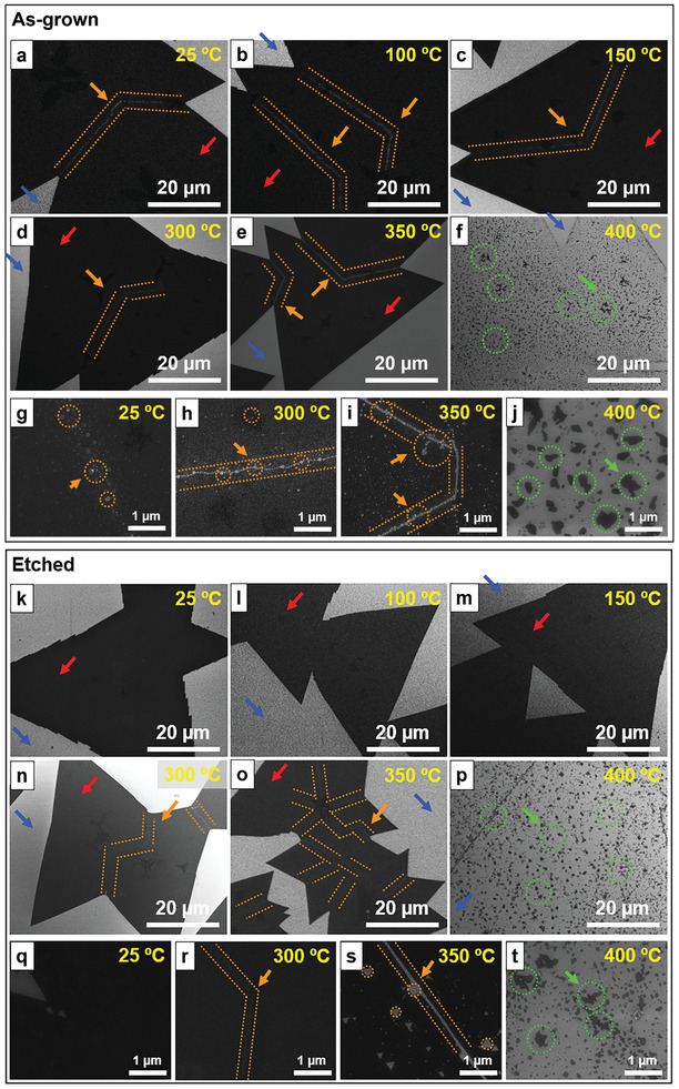
SEM images of the as‐grown and etched MoS2 monolayers before (25 °C) and after annealing (100–400 °C). a–j) The SEM images of the as‐grown MoS2 monolayers a,g) before annealing (25 °C) and after annealing at b) 100 °C, c) 150 °C, d,h) 300 °C, e,i) 350 °C, and f,j) 400 °C. k–t) The SEM images of the k,q) etched MoS2 monolayers before annealing (25 °C) and after annealing at l) 100 °C, m) 150 °C, n,r) 300 °C, o,s) 350 °C, and p,t) 400 °C. The light background is the SiO2/Si wafer (blue arrow) and monolayer MoS2 appears as a dark flake (red arrow). The bright nanoparticles (enclosed by orange dotted lines and pointed by arrows) are ascribed as MoOx nanoparticles. Both the f) as‐grown and p) etched MoS2 monolayers break into small pieces (green arrow and dotted circles) after being annealed at 400 °C. Ex situ SEM images were taken from different spots in different samples.
Figure 2.
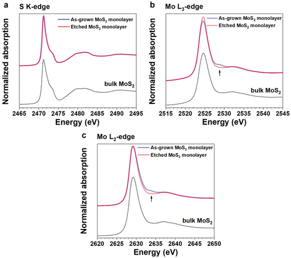
S K‐edge and Mo L2,3‐edges XANES spectra of the as‐grown and etched MoS2 monolayers with the bulk MoS2 reference. a) The S K‐edge, b) Mo L3‐edge, and c) Mo L2‐edge XANES spectra of the as‐grown (blue) and etched (red) MoS2 monolayers, and bulk MoS2 standard reference (black dot) are measured at room temperature (RT) under He atmosphere before oxidation. b,c) The additional shoulder peaks on the Mo L3 and L2‐edge spectra at b) 2528.6 eV and c) 2633.5 eV, respectively, (black arrows) from the as‐grown monolayer MoS2 indicate that the as‐grown monolayer MoS2 contains MoOx. The MoOx can be successfully removed from MoS2 monolayers by the alkaline bath treatment, which is confirmed through the removal of the additional shoulder peaks.
The operando XAS characterization reveals the details of the oxidation behavior differences for MoS2 monolayers with and without MoOx, which are not captured by SEM images. Our new operando XAS reactor equipped with EY detection mode enables, for the first‐time, XAS measurement of atomically thin MoS2 monolayers under reactive conditions (see the experimental scheme of the reactor in Figure S7 and Table S2, Supporting Information). The X‐ray beam spot size of 1 mm (vertical) × 3 mm (horizontal) is much larger than the single crystalline domain size of the monolayers (tens to around 100 µm). First, X‐ray absorption near edge structure (XANES) spectra of reference standards were obtained in the EY mode under He atmosphere under ambient pressure at RT using commercial bulk MoS2, MoO2, and MoO3 materials. The obtained spectra are consistent with the literature and our theoretical calculations (Figures S8 and S9, Supporting Information). Then, the S K‐edge and Mo L3,2‐edge XANES spectra of the as‐grown and etched MoS2 monolayers were measured under He atmosphere at RT. Though their spectra are similar to the bulk MoS2 material as shown in Figure 2, the as‐grown MoS2 monolayer shows additional shoulder peaks (black arrows) at 2528.6 eV in the Mo L3‐edge (Figure 2b) and 2633.5 eV in the Mo L2‐edge (Figure 2c), which indicates the presence of MoOx.
After confirmation of the existence of MoOx in the as‐grown MoS2 monolayers, operando XAS under the oxidative atmosphere was performed to follow the differences between the as‐grown and etched MoS2 monolayers with increasing temperature. The oxygen partial pressure used in the operando XAS electron yield reactor (3 vol% O2/He, 101.3 kPa) was identical to that used for the ex situ XAS, SEM, and XPS studies. The MoS2 monolayers were ramped to the desired temperature and held there for 30 min. Then, three consecutive overlapping XAS scans were recorded that show spectra reproducibility (Figure S10, Supporting Information), and the averaged spectra are used here. Figure 3 shows the operando XANES spectra of as‐grown (Figure 3a,c) and etched (Figure 3b,d) MoS2 monolayers under increasing temperatures (100–400 °C). The chemical evolutions of the as‐grown and etched MoS2 samples were monitored by following the S K‐edge (Figure 3a,b) and Mo L3‐edge (Figure 3c,d) XANES spectra.
Figure 3.
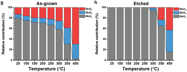
The operando S K‐edge and Mo L3‐edge XANES spectra of the as‐grown and etched MoS2 monolayers under dilute oxidative atmosphere (3 vol% O2/He) with increasing temperature (100–400 °C). a,b) The operando S K‐edge XANES spectra of the a) as‐grown and b) etched MoS2 monolayers are shown. The spectra of the commercial bulk MoS2 are included as references. The peak of S6+ is denoted at 2482.6 eV. c,d) The operando Mo L3‐edge XANES spectra of the c) as‐grown and d) etched MoS2 monolayers are shown. The prominent peak at 2528.6 eV generated by the gradual formation of MoO3 is marked with black arrows. The spectra of the commercial MoO2 and MoO3 are included as references. e,f) The difference spectra of the Mo L3‐edge XANES spectra of the e) as‐grown and f) etched MoS2 monolayers are shown. The spectra of the commercial MoO2 and MoO3 are included as references. g,h) The chemical compositions of g) as‐grown and h) etched MoS2 monolayers after oxidation at different temperatures are estimated from linear combination fitting analysis (LCFA).
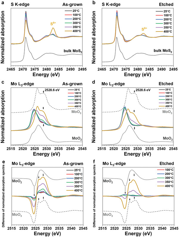
The evolution of the S K‐edge spectra is similar for the MoS2 monolayers with and without oxides. Both S K‐edge spectra features of the as‐grown and etched MoS2 monolayers match with the bulk MoS2 references for temperatures up to 350 °C, indicating that S atoms remain in the MoS2 chemical composition (Figure 3a,b). At 400 °C, both S K‐edge spectra show a new peak at 2482.6 eV, which is ascribed to S6+, likely in the form of sulfates.[ 31 ] The difference in the intensity of the new S6+ peaks at 400 °C indicates that the as‐grown sample oxidizes more than the etched monolayer MoS2 (Figure 3a,b). The formation of sulfates at 400 °C coincides with the severe morphological changes observed via SEM images (Figure 1f,p).
On the other hand, the operando Mo L3‐edge XANES spectra show different evolution features between the as‐grown and etched MoS2 monolayers (Figure 3c,d). Those spectra were further subtracted by the spectra of the etched monolayer at 25 °C (i.e., pristine MoS2 without oxides) to obtain the difference spectra (Figures 3e,f), which highlight the changes of spectra feature. For the as‐grown MoS2 monolayer, the first negative broad feature at 2524.5 eV ascribed to a combination of Mo4+ and Mo6+ grows with increasing temperature up to 300 °C. Then, the negative feature shifts 0.3 eV to lower energy, resembling Mo6+ as in the MoO3 reference (Figure 3e). Likewise, the Mo L3‐edge spectra show a gradually increased Mo6+ peak at 2528.6 eV with increasing temperature (Figure 3c,e). Finally, the Mo L3‐edge white line is shifted from resembling MoS2 to MoO3 at 400 °C (Figure 3c,e). In comparison, for the etched sample, the Mo4+ and Mo6+ peaks ascribed to MoO2 and MoO3 become slightly apparent only at 300 °C, and the Mo L3‐edge white line is shifted from resembling MoS2 to MoO3 at 400 °C (Figure 3d,f). The Mo L2‐edge spectra show the same trends (Figure S11, Supporting Information). We cross‐checked the operando XAS results by conducting ex situ XAS of those MoS2 monolayers shown in Figure 1, and the results are consistent (Figure S12, Supporting Information). First‐principles simulations of XAS spectra with the OCEAN code[ 32 , 33 ] show that O‐substitution on S‐vacancies in MoS2 monolayers produces a sequential shift of the absorption edge with increasing oxygenation as observed in our experimental spectra (Figure 3c,e; Figure S13, Supporting Information). To summarize the Mo L3‐edge operando XANES results, oxygenated Mo4+ and Mo6+ species are formed starting at 100 °C in the as‐grown MoS2 monolayer sample, and those species increase with increasing temperature (likely in the form of MoO2 and MoO3). In contrast, features ascribed to oxides start to appear at 300 °C for the etched MoS2 monolayer sample. Furthermore, the as‐grown MoS2 monolayers are nearly completely oxidized at 400 °C, at which point, Mo6+ species (as in MoO3) dominate the spectra; however, the etched MoS2 monolayers still show a transition towards MoO3 formation at 400 °C likely resulting in the spectral combination of MoO2 and MoO3 signals.
To quantitatively investigate the trend of chemical composition changes of the as‐grown and etched MoS2 monolayers at different temperatures, the linear combination fitting analysis (LCFA) of the operando Mo L3‐edge XANES from Figure 3c,d was performed,[ 34 ] and the results are presented in Figure 3g,h (see Tables S3 and S4, Supporting Information, for details). First, the chemical analysis supports the existence of MoOx in the as‐grown MoS2 monolayer, and on the contrary, the etched sample is composed of pure MoS2. Second, the amount of MoOx in the as‐grown sample is found to gradually increase with increasing temperature even at the low temperature of 100 °C, indicating the oxidation onset temperature (1% ± 1% MoO2 and 3% ± 1% MoO3 increase, and 5% ±1% MoS2 decrease). Third, the oxidation of the etched MoS2 monolayer starts at 300 °C. Complementarily, the normalized sulfur concentration acquired from the S K‐edge step as a function of temperature is shown in Figure S14, Supporting Information. The analysis of the edge step in the S K‐edge XANES spectra shows that both the as‐grown and etched MoS2 monolayers start losing significant amounts of S at around 350 °C, indicating that rapid oxidation happens. Both as‐grown and etched MoS2 monolayers undergo severe chemical transformations at 400 °C. The as‐grown monolayer MoS2 loses on average ≈23% more sulfur than the etched MoS2 monolayer under the same high temperatures and oxidation conditions at 350 and 400 °C. Overall, the differences between the samples in XANES and the chemical analysis suggest that the presence of MoOx lowers the onset temperature for fast thermal oxidation, promotes the oxidation reaction under the same temperature, and facilitates the sulfur loss in monolayer MoS2. Building upon published literature on the catalytic properties of oxides of molybdenum,[ 20 , 21 ] we propose that MoOx facilitates O2 dissociation ultimately lowering the onset oxidation temperature of as‐grown MoS2 monolayers down to 100 °C.
We further conducted complementary ex situ XPS at the O 1s, Mo 3d, and S 2p regions to confirm the impact of MoOx on the oxidation process of MoS2 monolayers. Figure 4a,d shows the O 1s spectra of the as‐grown and etched MoS2 monolayers that are fitted with two singlets, respectively. The main peak at 533.4 eV for both samples is assigned to Si–O from the SiO2/Si substrate.[ 35 ] The small peak at 531.4 eV corresponds to lattice Mo–O in oxide structures.[ 12 , 36 , 37 ] For the as‐grown MoS2 monolayer, the O 1s peak intensity of Mo–O gradually increases from RT to 400 °C, so does the Mo6+ peaks at 236.5 eV (3d3/2) and 233.5 eV (3d5/2) in the Mo 3d region (Figure 4b).[ 12 , 38 , 39 ] For the etched‐MoS2 layers, both the O 1s peak for Mo–O and the Mo6+ peaks are negligible below 300 °C (Figure 4d,e). The S 2p spectra show no significant differences throughout the oxidation process until 400 °C for both as‐grown and etched samples (Figure 4c,f). For both as‐grown and etched samples, the MoS2 monolayers seem to be nearly fully oxidized at 400 °C (Mo6+ ≈>90%, Figure S15, Supporting Information), as evidenced by the weak intensity of S 2p (Figure S16, Supporting Information; ten times magnified counts than in Figure 4f) and 2s peaks, and Mo4+ peaks at 233.3 eV (3d3/2) and 230.2 eV (3d5/2) in the Mo 3d region.[ 12 , 38 , 39 ] The XPS results support the observations from the operando XANES spectra (Figure 3) in that MoOx activates the oxidation of MoS2 monolayer from the low temperature at 100 °C. Nevertheless, operando XANES shows advantages by providing quantitative and qualitative information of chemical changes with better sensitivity, such as the sulfur loss and chemical specificity with increasing temperature under reactive and dynamic environmental conditions. Ultimately, operando XAS provides the accurate chemical composition evolution of the reaction products under the actual working conditions of 2D devices.
Figure 4.
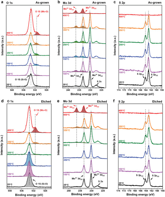
XPS spectra of O 1s, Mo 3d, and S 2p regions of the as‐grown and etched MoS2 monolayers before (25 °C) and after annealing (100–400 °C). a,d) XPS spectra of O 1s region of the a) as‐grown and d) etched MoS2 monolayers. The O 1s spectra are noted and partially fitted with the Mo–O (filled color with lines) and Si–O (filled color with dots) peaks. b,e) XPS spectra of Mo 3d region of the b) as‐grown and e) etched MoS2 monolayers. The Mo 3d spectra are noted and partially fitted with Mo6+ 3d3/2 and 3d5/2 peaks (filled color with lines). The other prominent peaks such as Mo4+ 3d3/2 and 3d5/2, and S 2s are denoted in each peak energy position. c,f) XPS spectra of the S 2p region of the c) as‐grown and f) etched MoS2 monolayers. The prominent peaks of S 2p1/2 and 2p3/2 are denoted in each peak energy position.
In summary, we reveal for the first time the low‐temperature thermal oxidation of monolayer MoS2 promoted by MoOx. Our pioneering ultrasensitive operando XAS study shows that the as‐grown MoS2 monolayers (via CVD) contain MoO2 and MoO3 impurities (i.e., MoOx) and that the amount of the oxides increases with increasing MoS2 oxidation even with exposures to diluted O2 at the low temperature of 100 °C (3 vol% O2/He, 101.3 kPa). In comparison, the etched MoS2 monolayers remain pristine until heating to 300 °C. The difference indicates that MoOx promotes the oxidation of MoS2 monolayers under the operation conditions of 2D devices. The available S atoms remain in a similar chemical and structural environment up to 350 °C, at which point MoS2 oxidizes to MoO3 and other volatile species. These results are supported by systematic ex situ XAS, XPS, and SEM characterizations. The results demonstrate that the oxide‐free condition is critical to the long‐term thermochemical stability of monolayer MoS2, which is expected to hold for other transition metal dichalcogenides monolayers with crucial implications for emerging scalable 2D electronic, optical, and catalytic applications.
Conflict of Interest
The authors declare no conflict of interest.
Supporting information
Supporting Information
Acknowledgements
S.P. and A.T.G.‐E. contributed equally to this work. The authors acknowledge the financial support of the Stanford Precourt Institute for Energy and Stanford Natural Gas Initiative. S.P. acknowledges the generous financial support from the Kwanjeong Educational Foundation. Use of the Stanford Synchrotron Radiation Lightsource, SLAC National Accelerator Laboratory, was supported by the U.S. Department of Energy, Office of Science, Office of Basic Energy Sciences under contract no. DE‐AC02‐76SF00515. Part of this work was performed at the Stanford Nano Shared Facilities (SNSF)/Stanford Nanofabrication Facility (SNF), supported by the National Science Foundation under award ECCS‐1542152. This research used resources of the National Energy Research Scientific Computing Center (NERSC), a U.S. Department of Energy Office of Science User Facility operated under contract no. DE‐AC02‐05CH11231. A.G. thanks the support by the U.S. Department of Energy, Office of Science, Office of Basic Energy Sciences, Chemical Sciences, Geosciences, and Biosciences Division, Catalysis Science Program to the SUNCAT Center for Interface Science and Catalysis.
Park S., Garcia‐Esparza A. T., Abroshan H., Abraham B., Vinson J., Gallo A., Nordlund D., Park J., Kim T. R., Vallez L., Alonso‐Mori R., Sokaras D., Zheng X., Operando Study of Thermal Oxidation of Monolayer MoS2 . Adv. Sci. 2021, 8, 2002768. 10.1002/advs.202002768
Contributor Information
Dimosthenis Sokaras, Email: dsokaras@slac.stanford.edu.
Xiaolin Zheng, Email: xlzheng@stanford.edu.
Data Availability Statement
Research data are not shared.
References
- 1. Radisavljevic B., Radenovic A., Brivio J., Giacometti V., Kis A., Nat. Nanotechnol. 2011, 6, 147. [DOI] [PubMed] [Google Scholar]
- 2. Lee J., Pak S., Giraud P., Lee Y. W., Cho Y., Hong J., Jang A. R., Chung H. S., Hong W. K., Jeong H. Y., Shin H. S., Occhipinti L. G., Morris S. M., Cha S., Sohn J. I., Kim J. M., Adv. Mater. 2017, 29, 1702206. [DOI] [PubMed] [Google Scholar]
- 3. Hill H. M., Rigosi A. F., Rim K. T., Flynn G. W., Heinz T. F., Nano Lett. 2016, 16, 4831. [DOI] [PubMed] [Google Scholar]
- 4. Sangwan V. K., Lee H. S., Bergeron H., Balla I., Beck M. E., Chen K. S., Hersam M. C., Nature 2018, 554, 500. [DOI] [PubMed] [Google Scholar]
- 5. Akinwande D., Petrone N., Hone J., Nat. Commun. 2014, 5, 5678. [DOI] [PubMed] [Google Scholar]
- 6. Park M., Park Y. J., Chen X., Park Y. K., Kim M. S., Ahn J. H., Adv. Mater. 2016, 28, 2556. [DOI] [PubMed] [Google Scholar]
- 7. Kang K., Xie S., Huang L., Han Y., Huang P. Y., Mak K. F., Kim C. J., Muller D., Park J., Nature 2015, 520, 656. [DOI] [PubMed] [Google Scholar]
- 8. Shim J., Bae S.‐H., Kong W., Lee D., Qiao K., Nezich D., Park Y. J., Zhao R., Sundaram S., Li X., Yeon H., Choi C., Kum H., Yue R., Zhou G., Ou Y., Lee K., Moodera J., Zhao X., Ahn J.‐H., Hinkle C., Ougazzaden A., Kim J., Science 2018, 362, 665. [DOI] [PubMed] [Google Scholar]
- 9. Kang K., Lee K. H., Han Y., Gao H., Xie S., Muller D. A., Park J., Nature 2017, 550, 229. [DOI] [PubMed] [Google Scholar]
- 10. Yalon E., McClellan C. J., Smithe K. K. H., Munoz Rojo M., Xu R. L., Suryavanshi S. V., Gabourie A. J., Neumann C. M., Xiong F., Farimani A. B., Pop E., Nano Lett. 2017, 17, 3429. [DOI] [PubMed] [Google Scholar]
- 11. Mak K. F., McGill K. L., Park J., McEuen P. L., Science 2014, 344, 1489. [DOI] [PubMed] [Google Scholar]
- 12. Sim D. M., Kim M., Yim S., Choi M.‐J., Choi J., Yoo S., Jung Y. S., ACS Nano 2015, 9, 12115. [DOI] [PubMed] [Google Scholar]
- 13. Spychalski W. L., Pisarek M., Szoszkiewicz R., J. Phys. Chem. C 2017, 121, 26027. [Google Scholar]
- 14. Yamamoto M., Einstein T. L., Fuhrer M. S., Cullen W. G., J. Phys. Chem. C 2013, 117, 25643. [Google Scholar]
- 15. Ly T. H., Chiu M.‐H., Li M.‐Y., Zhao J., Perello D. J., Cichocka M. O., Oh H. M., Chae S. H., Jeong H. Y., Yao F., Li L.‐J., Lee Y. H., ACS Nano 2014, 8, 11401. [DOI] [PubMed] [Google Scholar]
- 16. Szoszkiewicz R., Rogala M., Dabrowski P., Materials 2020, 13, 3067. [DOI] [PMC free article] [PubMed] [Google Scholar]
- 17. Park S., Siahrostami S., Park J., Mostaghimi A. H. B., Kim T. R., Vallez L., Gill T. M., Park W., Goodson K. E., Sinclair R., Zheng X., Adv. Mater. 2020, 32, 2003020. [DOI] [PubMed] [Google Scholar]
- 18. Zhang X., Grajal J., Vazquez‐Roy J. L., Radhakrishna U., Wang X., Chern W., Zhou L., Lin Y., Shen P. C., Ji X., Ling X., Zubair A., Zhang Y., Wang H., Dubey M., Kong J., Dresselhaus M., Palacios T., Nature 2019, 566, 368. [DOI] [PubMed] [Google Scholar]
- 19. Bettis Homan S., Sangwan V. K., Balla I., Bergeron H., Weiss E. A., Hersam M. C., Nano Lett. 2017, 17, 164. [DOI] [PubMed] [Google Scholar]
- 20. Holm R. H., Chem. Rev. 1987, 87, 1401. [Google Scholar]
- 21. Arzoumanian H., Coord. Chem. Rev. 1998, 178–180, 191. [Google Scholar]
- 22. Zhang N., Li X., Ye H., Chen S., Ju H., Liu D., Lin Y., Ye W., Wang C., Xu Q., Zhu J., Song L., Jiang J., Xiong Y., J. Am. Chem. Soc. 2016, 138, 8928. [DOI] [PubMed] [Google Scholar]
- 23. Ruiz Puigdollers A., Schlexer P., Tosoni S., Pacchioni G., ACS Catal. 2017, 7, 6493. [Google Scholar]
- 24. Kepp K. P., Inorg. Chem. 2016, 55, 9461. [DOI] [PubMed] [Google Scholar]
- 25. Erbil A., Cargill I. G., Frahm R., Boehme R. F., Phys. Rev. B: Condens. Matter Mater. Phys. 1988, 37, 2450. [DOI] [PubMed] [Google Scholar]
- 26. Elam W. T., Kirkland J. P., Neiser R. A., Wolf P. D., Phys. Rev. B: Condens. Matter Mater. Phys. 1988, 38, 26. [DOI] [PubMed] [Google Scholar]
- 27. Moggridge G. D., Rayment T., Ormerod R. M., Morris M. A., Lambert R. M., Nature 1992, 358, 658. [Google Scholar]
- 28. Greegor R. B., Pingitore N. E. Jr., Lytle F. W., Science 1997, 275, 1452. [DOI] [PubMed] [Google Scholar]
- 29. Velasco‐Velez J.‐J., Wu C. H., Pascal T. A., Wan L. F., Guo J., Prendergast D., Salmeron M., Science 2014, 346, 831. [DOI] [PubMed] [Google Scholar]
- 30. Tyurin A. G., Prot. Met. 2003, 39, 367. [Google Scholar]
- 31. Risberg E. D., Jalilehvand F., Leung B. O., Pettersson L. G., Sandstrom M., Dalton Trans. 2009, 3542. [DOI] [PubMed] [Google Scholar]
- 32. Vinson J., Rehr J. J., Kas J. J., Shirley E. L., Phys. Rev. B: Condens. Matter Mater. Phys. 2011, 83, 115106. [DOI] [PMC free article] [PubMed] [Google Scholar]
- 33. Gilmore K., Vinson J., Shirley E. L., Prendergast D., Pemmaraju C. D., Kas J. J., Vila F. D., Rehr J. J., Comput. Phys. Commun. 2015, 197, 109. [Google Scholar]
- 34. Jeong E. S., Park C. I., Jin Z., Hwang I. H., Son J. K., Kim M.‐Y., Choi J.‐S., Han S.‐W., Catal. Lett. 2015, 145, 971. [Google Scholar]
- 35. Duarte H. A., Sad M. E., Apesteguía C. R., Catal. Today 2019, 356, 399. [Google Scholar]
- 36. Liu J., Tang S., Lu Y., Cai G., Liang S., Wang W., Chen X., Energy Environ. Sci. 2013, 6, 2691. [Google Scholar]
- 37. Guan D., Li J., Gao X., Yuan C., J. Power Sources 2014, 246, 305. [Google Scholar]
- 38. Kibsgaard J., Chen Z., Reinecke B. N., Jaramillo T. F., Nat. Mater. 2012, 11, 963. [DOI] [PubMed] [Google Scholar]
- 39. Gao J., Li B., Tan J., Chow P., Lu T. M., Koratkar N., ACS Nano 2016, 10, 2628. [DOI] [PubMed] [Google Scholar]
Associated Data
This section collects any data citations, data availability statements, or supplementary materials included in this article.
Supplementary Materials
Supporting Information
Data Availability Statement
Research data are not shared.


