Abstract
Graphene is ideally suited for optoelectronics. It offers absorption at telecom wavelengths, high-frequency operation and CMOS-compatibility. We show how high speed optoelectronic mixing can be achieved with high frequency (~20 GHz bandwidth) graphene field effect transistors (GFETs). These devices mix an electrical signal injected into the GFET gate and a modulated optical signal onto a single layer graphene (SLG) channel. The photodetection mechanism and the resulting photocurrent sign depend on the SLG Fermi level (EF). At low EF (<130 meV), a positive photocurrent is generated, while at large EF (>130 meV), a negative photobolometric current appears. This allows our devices to operate up to at least 67 GHz. Our results pave the way for GFETs optoelectronic mixers for mm-wave applications, such as telecommunications and radio/light detection and ranging (RADAR/LIDARs.)
Subject terms: Optics and photonics, Optical properties and devices
Here, the authors report optoelectronic mixing up to 67 GHz using high-frequency back-gated graphene field effect transistors (GFETs). These devices mix an electrical signal injected into the GFET gate and a modulated optical signal onto a single layer graphene channel.
Introduction
Mixers are a key component of modern communication modules1. In telecommunications and in radio detection and ranging (RADAR) systems2, the receiver analyzes the modulation of a carrier wave (or waveform) with frequencies in the microwave (3–30 GHz) or mm-wave (30–300 GHz) range, to extract information3,4. As signal processing is performed at near-zero frequencies (baseband3,4), frequency downconversion is required3,4. Downconversion is performed by mixing the modulated high-frequency signal centered around the radio frequency (RF) carrier frequency, fRF, with a local oscillator signal at frequency fLO. This translates the modulation centered around fRF to fIF = fLO − fRF. The local oscillator frequency is typically set near fRF, so that fIF is close to zero3,4. Superheterodyne receivers are a common type of radio receivers using frequency downconversion to process the original signal5. For multi-antenna systems, it is preferable to use a single optical signal as a local oscillator and distribute it to each antenna6, decreasing the receiver complexity and noise. For this purpose, one option is to use photodetectors (PDs) to transfer the local oscillator signal from the optical to the electrical domain6. After that, an electrical mixer is used5. A second option is to employ optoelectronic mixers (OEMs)7, i.e., PDs capable of mixing optical local oscillator with an electrical signal7. OEMs are particularly convenient in RADAR and light detection and ranging (LIDAR) applications7–10. State-of-the-art OEMs at 1.55 μm are based on III–V semiconductors epitaxially grown on InP11,12. These are efficient, but expensive, and can only be heterogeneously integrated in an Si platform11,12. Low cost and complementary metal-oxide-semiconductor (CMOS) compatible OEMs require CMOS-compatible materials absorbing light at 1.55 μm13.
Graphene is promising for optoelectronics14–18, with mobilities up to ~150,000 cm2 V−1 s−1 at room temperature (RT)19, a short (~1 ps) photocarrier lifetime20–22, and a 2.3% broadband light absorption (including telecom wavelengths)23. Graphene-based optoelectronic devices are compatible with Si platforms16,24–27. Therefore, graphene-based OEMs could combine telecom operation and CMOS compatibility.
Low frequency (2MHz) optoelectronic mixing in single-layer graphene (SLG) was studied in ref. 28 using a transistor structure with an on-chip bias resistor. This reported upconversion of a 2MHz signal, and downconversion of a 0.45 MHz one, in two types of OEMs consisting of a SLG field-effect transistor (GFET) and a bias resistor. For the first, the oscillating electrical signal was applied to the GFET drain (the optical signal illuminated the GFET channel), whereas in the second the signal was applied to the gate, and the mixing was proportional to the on-chip resistance. A 30 GHz bandwidth (BW) OEM based on SLG was reported in ref. 29, based on an SLG coplanar waveguide (GCPW) integrating a SLG channel grown by chemical vapor deposition (CVD). The RF signal was injected into the GCPW, whereas a 1.55 μm laser illuminated the channel. Optoelectronic mixing was based on the linear dependence of the photocurrent on both optical incident power (Popt) and voltage drop (Vbias) along the channel. As the photocurrent is proportional to PoptVbias30, upconverted and downconverted signals were generated. This GCPW operated up to 30 GHz, with a conversion efficiency, (i.e., ratio of output power at fIF and input power at fRF), of −85 dB for a 10 GHz modulated signal. The results in ref. 29 are far from state-of-the-art OEM performances achieved with III–V semiconductor-based uni-traveling carrier photodiodes: −22 dB conversion efficiency at 35 GHz31, and −40 dB at 100 GHz12. However, the CMOS integration of III–V semiconductors is challenging13. SLG is CMOS-compatible16 but, to technologically bridge the gap with III–V-based OEMs, BW, and conversion efficiency need to be improved29. Furthermore, the OEM in ref. 29 was a two-contact device operating only in the photoconductive regime, at a fixed Fermi level (EF).
Here, we present a 67 GHz GFET-OEM (three-contact device), exploiting the modulation of EF, that controls the photoconductivity. At low (equilibrium) EF (<130 meV) the laser power induces interband transitions32, thus the charge carrier density, n, and the channel conductance increase (positive photoconductivity). At high EF (>130 meV), the laser heating induces intraband transitions32. In this case, the hot carrier distribution reduces the effectiveness of the electronic screening32 which, in turn, leads to a higher scattering rate (e.g., owing to Coulomb impurities32 or strain disorder33). The increased scattering decreases the carrier mobility32 and the resulting photoconductivity is negative32,34–36. In our OEMs, an intensity-modulated (up to 67 GHz) laser beam illuminates part of the SLG channel, generating an AC photocurrent, proportional to the product of optical power and photoresponsivity. An RF signal applied to the gate of 20 GHz-BW GFETs modulates the photoresponsivity, mixing optical and electrical signals. The performance far exceeds that in ref. 29. The conversion efficiency (−67 dB) for a 67 GHz modulated optical signal (fopt) is 21 dB higher than ref. 29 at fopt = 10 GHz, thanks to the use of an RF GFET with a strong coupling between the input RF signal and SLG (a 0.8 V signal induces EF ~ 0.2 eV). Our results pave the way for the use of graphene in CMOS-compatible OEMs.
Results
Graphene growth and characterization
SLG is grown via CVD on 35 μm-thick Cu foil, following ref. 37. The temperature, T, is raised to 1000 ∘C in an H2 atmosphere (~200 mTorr), and kept constant for 30 mins. In all, 5 sccm CH4 are then added to the 20 sccm H2 flow to start growth, for additional 30 mins at 300 mTorr. The sample is then cooled at ~1 mTorr to RT. We use Raman spectroscopy at 514nm to characterize the material. Figure 1a shows the Raman spectrum on Cu (red line), after Cu photoluminescence removal38. The D peak is absent, indicating negligible defects39,40. The 2D peak at ~2705 cm−1 is a single Lorentzian with full width at half maximum (FWHM) ~31 cm−1, a fingerprint of SLG41. The position of the G peak, Pos(G), is ~1593 cm−1, with FWHM(G) ~12 cm−1. The 2D to G intensity and area ratios are I(2D)/I(G) ~ 2.4, A(2D)/A(G) ~ 6.3.
Fig. 1. SLG Raman characterization and device description.
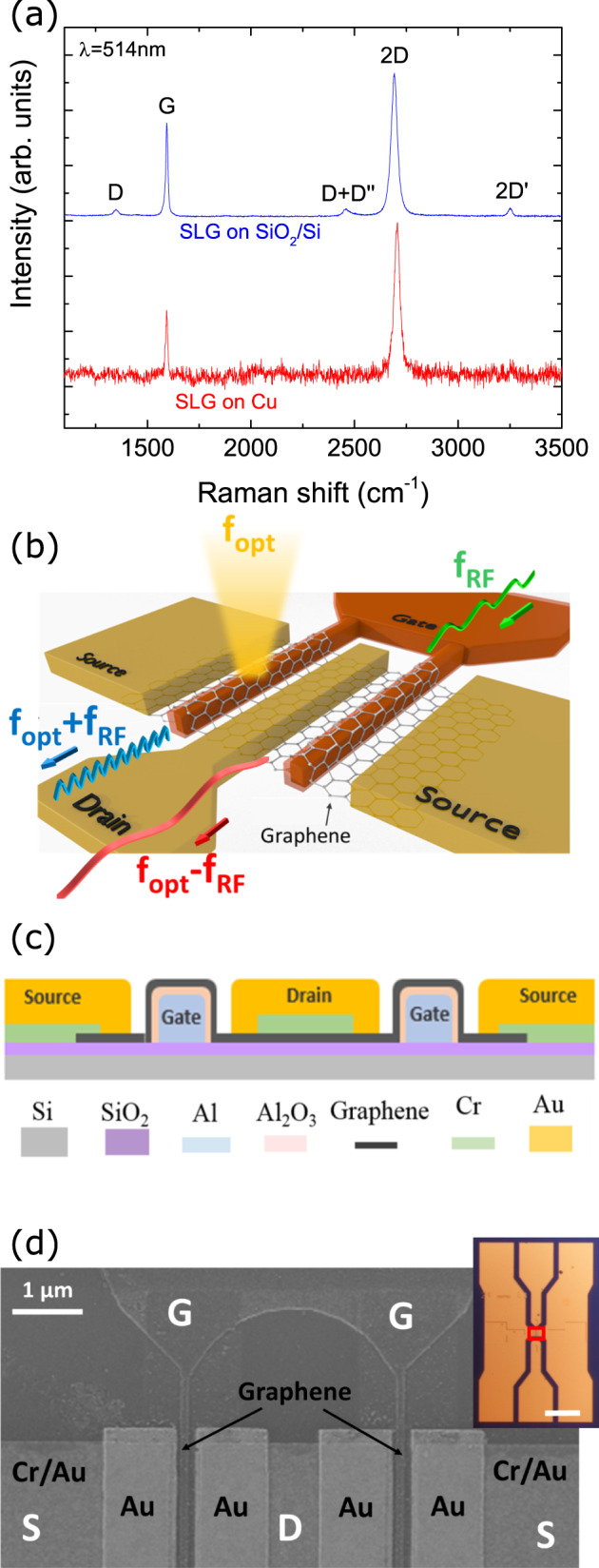
a Representative Raman spectra at 514 nm of SLG as-grown on Cu (red), and after transfer on SiO2/Si (blue). b Principle of operation of our OEM. The mixing of the electrical signal at fRF with the photodetected signal at fopt generates two signals at the output (drain): fopt + fRF and fopt − fRF. c Schematic GFET cross-section. The two Al gates (pale blue) are covered by a thin Al2O3 oxide (pink). SLG (black) is placed on the two gates. The drain and source contacts are Au (yellow) and Cr (green). d SEM image of GFET with dual-bottom gate finger covered by SLG. The metal in contact with SLG is Au. The inset shows the GFET (red rectangle) integrated into a coplanar waveguide (CPW) (scale bar: 100 μm).
To prevent ohmic losses at microwave frequencies, a high resistivity Si wafer (> 8000Ωcm) covered with 285nm SiO2 is used. SLG is wet transferred42,43 on it as follows. A poly(methyl methacrylate) (PMMA) layer is spin-coated on the surface of SLG/Cu and then placed in a solution of ammonium persulfate (APS) and deionized (DI) water for Cu etching42. The PMMA membrane with attached SLG is then immersed into a beaker filled with DI water for cleaning APS residuals. After, the PMMA/SLG stack is transferred onto the target substrate and the PMMA layer is removed. SLG is then ion etched to define the channel.
We then characterize via Raman spectroscopy the transferred SLG (blue curve, Fig. 1a). Both measurements on Cu and Si+SiO2 are performed under the same conditions of laser power, objective, wavelength, and accumulation time. The Raman signal of SLG on Cu is more noisy than on Si+SiO2 due to interference enhancement by the 300 nm SiO2 layer on Si44,45. For SLG on Si+SiO2 we have Pos(G) ~1594 cm−1, FWHM(G) ~11, Pos(2D) ~2691 cm−1, FWHM(2D) ~34 cm−1, I(2D)/I(G) ~1.6, A(2D)/A(G) ~4.5. This indicates p-doping ~300 meV46,47. I(D)/I(G) ~0.09 corresponds to a defect density ~4 × 1010 cm−240,48, consistent with what is commonly observed in CVD-SLG49. It is possible to improve the process to get a smaller D peak50.
Operational principle and device fabrication
Figure 1b is a sketch of our SLG OEM and illustrates its operational principle. It consists of a GFET with a symmetric dual-bottom gate finger. This layout is commonly used for RF applications51 and GFETs52, and is well suited for GCPWs53. Dual-gate finger FETs have a more compact design and a reduced small-signal gate resistance compared with single-gate configurations, for a given equivalent channel width, resulting in a higher voltage gain54. A laser beam is modulated at fopt and focused on the GFET channel. As a result, a photocurrent that contains an AC component at fopt flows through the SLG channel. If a RF signal fRF is applied to the gate, the output current presents a term at fRF. When both optical and electric signals are applied, the device acts as an OEM: the output contains the product of the two signals, and two AC components at fopt + fRF and fopt − fRF appear.
A schematic cross-section of the bottom gate GFET is in Fig. 1c. The fabrication starts by patterning the dual-bottom gate finger by e-beam lithography (EBPG 5000 Plus). The gates are made of a 40 nm-thick Al layer deposited by evaporation. A 4 nm Al2O3 layer is formed on top of the gates by exposing the substrate to pure oxygen for 30 mins55 with an Oxford Plasmalab80Plus at ~100 mTorr. This thin oxide acts as gate dielectric. The source and drain contacts are made in a two-steps process. First, Cr/Au (5/50 nm) pre-contacts are deposited on SLG. Then, ohmic contacts are obtained by placing 30 nm Au on the Cr/Au-SLG junction. Finally, a CPW is built with a Ni/Au film (50/300 nm). Figure 1d is a scanning electron microscopy (SEM) image of the bottom gates covered by SLG. The inset shows a GFET integrated into the CPW. The red square indicates the area occupied by the GFET. The bottom gate GFET design is suitable for OEMs since (1) the SLG channel is on the gate and can be directly illuminated; (2) the use of a thin (4 nm) Al2O3 dielectric and short gate (<0.4 μm or less) ensures high-frequency operation5,56,57.
The device has a cutoff frequency (not de-embedded) ft ~ 25 GHz, and a maximum oscillating frequency fmax ~ 14GHz, as deduced from the S-parameters measured with a Vector Network Analyzer (VNA, Agilent, E8361A). To calibrate the VNA, we use the Line-Reflect-Reflect-Match approach58. This allows us to eliminate errors in S-measurements introduced by the environment, such as cables and probe tips used to contact the device under test, and the VNA non-idealities.
Electrical and optoelectronic measurements
The setup in Fig. 2a is used to measure photocurrent and optoelectronic mixing. The output of a 1.55 μm distributed feedback laser is modulated by a Mach Zehnder modulator in the double sideband suppression carrier mode59, to obtain a modulated beam at fopt. This is then amplified with an Erbium-doped fiber amplifier. The maximum fopt that our setup can probe is 67 GHz. The diameter of the focused laser spot is ~2 μm (inset of Fig. 2a). The maximum power impinging on the sample is ~60 mW, which corresponds to ~20 mW/μm2. The gate and drain are connected to a VNA with two high-frequency (67 GHz) air coplanar probes. Bias tees are used to add a DC bias to channel and gate electrodes, and to measure the DC currents and voltages with a Source-Measure-Unit (Keithley 2636B). After illuminating the device, we verify the stability of the signal before measuring the RF photocurrent, whereas monitoring the DC value of the channel resistance, to ensure that no damage nor significant modification is induced by the laser power or DC bias. We do not observe any degradation or time-dependent drift in the DC or RF currents over a period of at least 3 h, the typical measurement time.
Fig. 2. Measurement setup and device characteristics.
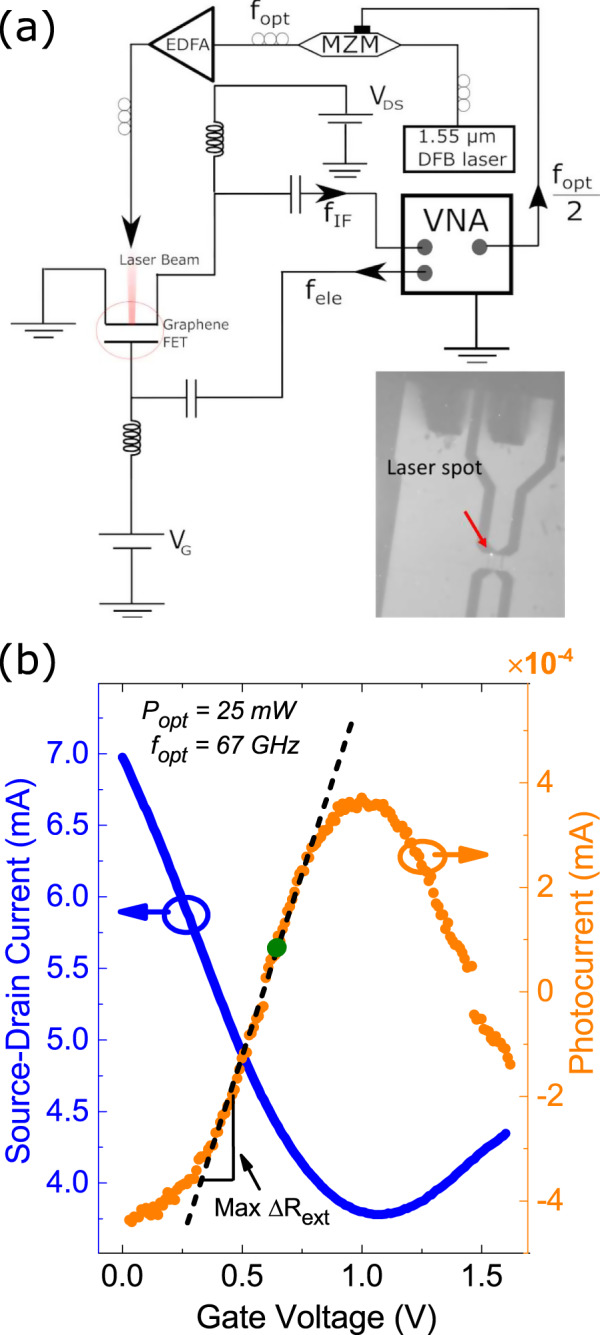
a Experimental setup: a CW laser is modulated via a MZM. It is then amplified with an EDFA and focused on the GFET. An AC signal is applied to the gate. The output fIF is measured on a VNA. Inset: optical image of device with laser focused on the channel. b Blue curve: source-drain current versus gate voltage, for VDS = 200 mV. Orange curve: photocurrent versus gate voltage, generated by a 25 mW beam focused on the SLG channel.
We now present the results for a representative OEM with SLG channel width W = 24 μm, length L = 400 nm, and gate length LG = 200 nm. The blue curve in Fig. 2b is the source-drain current, IDS, as a function of gate voltage, VGS, at VDS = 200 mV, which shows the typical ambipolar conduction behavior of a GFET (i.e, electrical conductivity due to electrons/holes (e/h), depending on the position of EF with respect to the charge neutrality point, CNP)60. The minimum conductance is reached at VGS = 1.1 V, which corresponds to the CNP voltage (VCNP). When VGS increases (decreases) with respect to VCNP, the e(h) density increases, leading to a reduction of channel resistivity, so an increase of the current flowing in the channel60. μ is calculated as μ = Lgm/(W ⋅ CGVDS)61. The transconductance gm = dIDS/dVGS13 is obtained from the transfer characteristic IDS(VGS) at VDS = 10 mV. The gate capacitance is Cox is ~5 fF/μm, obtained from S parameters measurements on 60 devices of the same kind55. We get μ ~ 2500 cm2 V−1 s−1, consistent with that of non-encapsulated CVD-SLG37.
We now consider the photoresponse. The OEM is biased at VDS = 200 mV and illuminated with a laser modulated at fopt = 67 GHz. The electrical power PRF measured by the VNA is used to derive the photocurrent Iph. From Joule’s law13 , with ZVNA = 50 Ω the VNA input impedance. The use of bias tees allows us to simultaneously measure the DC component, i.e., the dark current (blue curve in Fig. 2b) and the AC component, i.e., the photocurrent (orange curve in Fig. 2b) as a function of VGS, for a 25 mW incident optical power. The photocurrent, Iph, sign depends on VGS. Iph is positive and has a local maximum close to the CNP. At low (equilibrium) EF (<130 meV), the laser power induces interband heating32, thus an increase of n (positive photoconductivity). Therefore, the photocurrent has the same sign as the DC current in the channel, owing to the DC bias. At high EF > 130 meV, the sign of the photocurrent is opposite to the DC current (negative photoconductivity). In this case, laser heating induces intraband transitions, which lead to a reduction of electronic screening of the long-range Coulomb interaction between SLG’s carriers and charged impurities in the substrate22,32. The EF at which the transition between positive and negative photocurrent takes place is ~0.1–0.2 eV32,34. The value depends on the charge transport scattering rate in SLG, i.e., the mean time interval between two collisions in the diffusive transport picture62, and on the charge neutrality region width63 (see Methods). In our experiment, we observe this transition at ~130 meV.
The external photoresponsivity, Rext, is defined as15,64 Rext = , with = 31%Pcw the fraction of the optical power coupled to the SLG channel. We get Rext ~ 0.22 mA/W. For VGS = 0V, the device reaches its maximum Iph ~ −4.2 × 10⁻⁴ mA and the photocurrent generated by a 67 GHz laser modulation is measured as a function of DC bias and optical power.
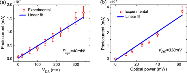
Figures 3a, b plot the photocurrent as a function of DC bias at Popt = 40 mW and as a function of the optical power for VDS = 330 mV. The response is linear in both cases, as expected for a photoconductor34. The frequency response of the photodetected power is then measured as a function of fopt, Fig. 4a. We get a flat response over the whole band that can be investigated by our VNA, showing that the intrinsic photodetection BW is >67 GHz. The photocurrent can originate from the SLG channel located above the gate, or from the SLG-metal contacts that are not gated (see Fig. 1c). As the photoresponse strongly depends on VGS, as shown in Fig. 2b, we ascribe it to the illuminated part of the SLG channel located above the gate. If both contacts are illuminated, the photocurrents are opposite and cancel out. If the photocurrent originates mainly from one SLG-metal contact, the photocurrent at VDS = 0V should be significant. Rext ~ 0.8 mA/W was reported in ref. 65 for a detector exploiting the metal-SLG contacts, at VDS = 0V. As seen in Fig. 3, at VDS = 0V the photocurrent is negligible. We also rule out possible asymmetric heating effects on the channel, owing to beam location, by performing a photocurrent measurement as a function of laser spot position. We observe a very weak response at VDS = 0V, regardless of laser spot position, as shown in Methods, Fig. 10. Thus, the role of contacts can be neglected.
Fig. 3. Photocurrent measurements.
a Photocurrent as a function of VDS at 40 mW optical power, b photocurrent as a function of the optical power, at VDS = 330 mV. Error bars are obtained from the VNA measurement noise standard deviation.
Fig. 4. RF Optoelectronic characterization.
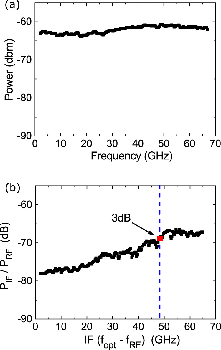
a Maximum photodetected power at VGS = 0V, VDS = 330 mV, as a function of fopt. b PIF/PRF at VGS = 0.6V, VDS = 330 mV. Optical power in a, b is 60 mW.
Fig. 10. Photoresponse as a function of laser spot position.
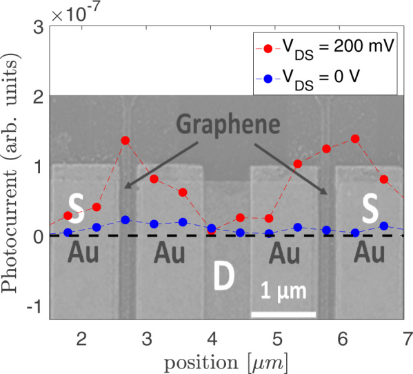
The red and blue curves show the measured photoresponse as a function of laser spot position along the black dashed cut line, at 200 mV and 0 V, respectively.
In order to operate the device as an OEM (instead of a PD), an RF signal fRF is added to the DC gate, Fig. 1b. fopt is maintained at 67 GHz, whereas fRF is swept between 2 and 65 GHz. A VNA is used to record PIF and the transistor power at the intermediate frequency fIF = fopt−fRF.
An important parameter for OEMs is the downconversion efficiency5: PIF/PRF, with PRF the power at the source and PIF that measured at the VNA. For our device, the maximum PIF/PRF is −67 dB at VGS = 0.6 V. For this VGS, Fig. 4b plots PIF/PRF as a function of fIF. The BW and PIF/PRF of our OEMs far exceed (+37 GHz in BW and 2 orders of magnitude in PIF/PRF) those of ref. 29, where the input RF signal modulates the SLG bias (resistive coupling), thus the photocurrent amplitude. In our OEMs, the input RF signal is coupled to SLG via the gate oxide (capacitive coupling), which results in a modulation of EF and, consequently, in a change of the photocurrent mechanism and sign. These high BW and PIF/PRF come from the strong coupling (i.e., strong electric field for a small applied voltage, 0.25 V/nm) between the input RF signal (applied to the Al back-gate) and the SLG channel, thanks to the use of a ~4 nm oxide. As a consequence, an efficient field effect is achieved60. A signal with an amplitude ~0.8 V induces a EF modulation ~0.2 eV. Thus, a small signal (0.8 V) is needed to obtain optoelectronic mixing. The high-frequency operation of the GFET (~20 GHz, 3 dB BW, Fig. 4b) comes from the short channel length (400 nm) and the small gate capacitance Cox ~ 60 fF66.
Figure 5a is a color map of the 67 GHz photocurrent as a function of VGS, VDS. We then add to the DC gate bias an electrical signal at 10 GHz. The resulting downconverted photocurrent at fIF = 57 GHz is plotted as a function of VDS, VGS in Fig. 5b. By differentiating the map in Fig. 5a with respect to VGS, we obtain Fig. 5c, which resembles Fig. 5b. This is best seen in Fig. 6, which plots both values as a function of VGS for VDS = 200 mV. The curves of the downconverted photocurrent and of the derivative of the photocurrent can be superposed. This result is valid regardless of frequency, see Methods Fig. 9.
Fig. 5. VGS–VDS maps.
a Photocurrent map as a function of VGS, VDS. b Downconverted photocurrent map as a function of VGS, VDS. c Derivative of a with respect to VGS. The photocurrent values are in mA.
Fig. 6. Downconversion efficiency vs VGS.
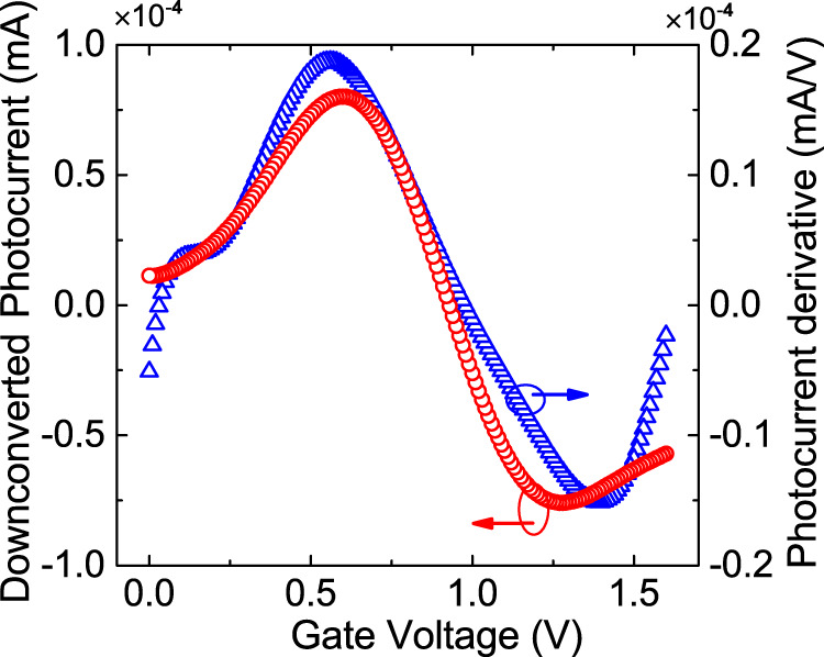
Red curve: cut of Fig. 5c for VDS = 200 mV. Blue curve: cut of Fig. 5b for VDS = 200 mV.
Fig. 9. Downconverted photocurrent versus gate voltage at different frequencies.
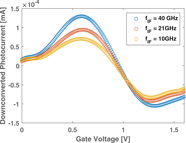
The three curves show the downconverted photocurrent at 10, 21, 40 GHz. The same behavior shown in Fig. 6 is observed, regardless of the operating frequency.
Discussion
This behavior can be explained by a small-signal analysis.
Let us consider the modulated optical power impinging on the PD, Popt = Pcw + Pmodsin(2πfoptt), with Pmod the amplitude of the varying part of the optical power. The photocurrent is proportional to Popt through the factor Rext. This depends on VGS, as for Fig. 2b, and is almost independent on fopt, Fig. 4a. Therefore, the photocurrent can be written as:
| 1 |
By applying to the gate a DC bias and a small signal , we get:
| 2 |
where
| 3 |
We include dependence on injected electrical frequency through a frequency-dependent proportionality constant β(fRF). The total photocurrent has four terms:
| 4 |
The first is the DC photocurrent. The second describes the DC photocurrent modulated by the electrical signal. The third represents the photocurrent modulated at fopt, Fig. 2b. The fourth describes the optoelectronic mixing and can be rewritten as:
| 5 |
Equation (5) has two components at fopt + fRF and fIF = fopt − fRF. It shows that the mixed signal depends exclusively on , i.e., on the derivative of Rext with respect to VGS, not on Rext itself, in accordance with Fig. 5. is maximum for VGS ~ 0.6 V, Fig. 6, i.e., in a region where the photocurrent changes sign, indicated in Fig. 2b with a green dot. The sharper is the transition between the two competing phenomena (photoconductive and bolometric) generating the photocurrent, the higher is and the optoelectronic-mixing efficiency.
Since Rext is proportional to the photoconductivity σph(VGS)30, the optimization of the mixing efficiency () requires to be maximized. σph(VGS) depends on several factors, such as the residual charge carrier density, n063, and the dominating scattering mechanisms63,67. So, it depends on SLG quality and its dielectric environment. We compute σph(VGS) from the Drude model for free carrier conductivity in SLG63:
| 6 |
where Te is the electron temperature, Γ is the scattering rate, D is the Drude weight63,67, and μc is the chemical potential. We calculate μc (see Methods for details), and then the effect of e-h puddles by replacing μc with 63, where is the energy width of the puddles region63. The photoconductivity due to illumination of the SLG channel at a given μc is then given by63:
| 7 |
where Tlight is the hot-electron temperature of the illuminated SLG and Tdark is the electron temperature in dark, see Methods for details. Figure 7 plots the measured photoconductivity (blue) and the computed one (red) using Eq. (7). We calculate Δμpuddles from n0, extracted from the experimental DC measurement of the conductivity (see Methods). We calculate Γ from the measured μ (see Methods). We get Γ ~ 50 meV, which corresponds to a scattering time τ ~ 80 fs at EF ~ 200 meV, at the maximum VGS, in agreement with experiments.
Fig. 7. Comparison between measured and calculated photoconductivity.
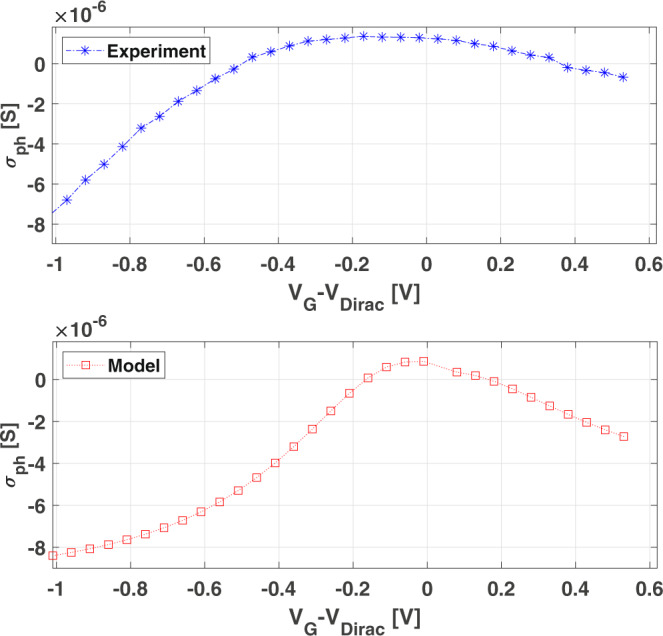
a Measured and b calculated photoconductivity of illuminated SLG channel.
We then calculate to find the maximum downconversion efficiency. This can be increased by ~27 dB (power unit) for SLG with μfe ~30,000 cm2 V−1 s−1 (τ = 1/Γ ~ 0.6 ps) and n0 ~ 1011 cm−2, see Methods. Thus, the control of the transition between the two different photocurrent mechanisms could lead to a maximization of and, in turn, a maximization of downconversion efficiency.
The 3 dB BW is ~19.7 GHz when operated as OEM, Fig. 4. This behavior is modeled in Eq. (3) by including the factor β(fRF). To understand the optoelectronic-mixing dependence on fRF and, thus, on fIF (fopt being fixed), we consider a typical figure of merit of high-frequency transistors: the transducer power gain5, defined as: GT = , where Pload is the power delivered to the load and Pavs is the source power. GT coincides with the modulus of the S21 parameter when source and load are matched5. This is the case in our measurements, where the power is delivered from the VNA 50Ω-source and measured on a 50Ω receiver. GT is close to the S21 parameters. An external impedance matching could increase the downconversion efficiency by maximizing the power delivered by the GFET, other than increasing BW. We do not observe saturation in the photodetected signal at the highest optical power available in our setup (60 mW). Thus, illuminating a wider channel surface, while maintaining the same optical power density, should increase the downconversion efficiency. An enhancement of SLG-light interaction can also improve the downconversion efficiency. In all, ~70% absorption could be achieved by integrating SLG on a waveguide68. This could enhance the downconversion efficiency by ~30 dB, compared with the normal incidence case (~2.3% absorption23).
In summary, we reported high-frequency graphene transistors operating as OEMs for frequencies up to at least 67 GHz. The photodetection BW exceeds 67 GHz. The BW of the devices operated as OEMs is 19.7 GHz. The conversion efficiency is at least two orders of magnitude higher than previous graphene OEMs29. It can be further increased using high-quality samples with μ ~ 10,000–100,000 cm2 V−1 s−1 and increasing light-matter interaction. This can increase the downconversion efficiency >50 dB, overcoming state-of the-art performances of OEMs based on any other technology31. Our frequency operation is already comparable with state-of-the-art performance of OEMs based on any other technology31. Thus, our work paves the way for the use of graphene-based transistors as OEMs in applications exploiting mm-waves, such as telecommunications and RADAR/LIDAR.
Methods
Photocurrent modeling
Equations 1–5 show that the optoelectronic-mixing efficiency is proportional to , which can be expressed as:
| 8 |
Since Rext is proportional to σph(VGS)30, the optimization of the mixing efficiency requires to be maximized. The mixing efficiency can be related via to SLG’s μ and n63,67. The Drude model for free carrier conductivity in SLG gives63:
| 9 |
In the case of Dirac Fermions the Drude weight is63:
| 10 |
with kB the Boltzmann constant. In the GHz range, ω ~ 109−1010 rad/s. This value is negligible compared to our Γ, which lies in the range 1012−1013 rad/s32. The photoconductivity owing to the illumination of the SLG channel is then 63:
| 11 |
This depends on T, as experimentally shown in ref. 34. Increasing T decreases the photodetection efficiency34. This is consistent with the screening reduction of the scattering mechanism while increasing Te32, since a smaller T change between dark and illumination conditions takes place.
μc is T-dependent. It decreases while increasing T to keep the number of conduction band carriers constant69. So, it is lower in illumination conditions with respect to dark. To account for this, we compute μc by numerical inversion of the following T-dependent formula60,63:
| 12 |
In Eq. (12), Cox is the geometrical gate capacitance per unit area, v0 is the Fermi velocity and Li2 is the dilogarithm function. This is valid in low and high doping and also includes the effects of quantum capacitance. Γ is calculated from μfe ~ 2500 cm2/(Vs) using16:
| 13 |
We get Γ ~ 80 meV, i.e. τ ~ 50 fs for μc ~ 0.2 eV. Charge puddles are taken into account by replacing μc with63:
| 14 |
Δμpuddles is calculated as60:
| 15 |
Here, n0 ~ 5 ⋅ 1011 cm−2 extracted from the measured DC minimum of conductivity σmin60:
| 16 |
From the DC measurements, we get Cox ~ 4fF/μm2. The experimental curve in Fig. 7 uses Te as a fitting parameter, getting Te ~ 320 K in the laser spot region.
Optoelectronic mixing efficiency
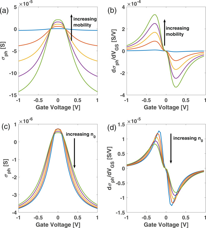
We now evaluate the effects of μ and n0 on mixing efficiency. Since our SLG is substrate-supported and not encapsulated in hBN, long-range scattering limits conductivity32, more specifically Coulomb scattering32,70,71. In this regime, the typical τ is in the range of hundreds of fs32. High-quality SLG can have low n0 (<1012 cm−2) and high μ > 100,000 cm2 V−1 s−1)50. In high-quality SLG encapsulated with hBN, as in ref. 50, transport is dominated by random-strain fluctuations33,72. For such SLG, a change in μ < 20% was measured as a function of n50. In order to estimate the performance in such SLG, we assume no dependence of μ o n. Within this assumption, τ ∝ μ for μ >> KBT60, so Eq. (13) is still valid. For μ ~ 100,000 cm2 V−1 s−1, τ can be up to 2ps for EF ~ 0.2 eV16. We thus calculate σph for μ up to 100,000 cm2 V−1 s−1 and n0 ~ 5 ⋅ 1011 cm−2, Fig. 8a. By comparing the green and the blue curves, which show the photoconductivity for μ ~ 100,000 and 2.500 cm2 V−1 s−1, we predict an increase ~40 times at both low (i.e. VGS = 0) and high electrostatic doping (i.e., for VGS = 1 V). We then differentiate the curves in Fig. 8a. Figure 8b shows an increase in dσph/dVGS, (i.e. an increase of ) of a factor ~40.
Fig. 8. Optoelectronic-mixing performance.
a Calculated photoconductivity and b photoconductivity derivative for μfe varying from 3800 to 100,000 cm2 V−1 s−1. c Calculated photoconductivity and d photoconductivity derivative for n0 varying from 1011 to 4.5.1011 cm−2.
Another parameter that can be improved by employing high-quality SLG is n0. Fig. 8c plots the photoconductivity for n0 between 1011 cm−2 (corresponding to high-quality SLG50) and 5 × 1011 cm−2 (our case), while keeping μfe = 2500 cm2 V−1 s−1. In this case, the photoconductivity increases by a factor ~1.4 near the CNP, as well as at high doping (VGS = 1 V), with dσph/dVGS almost doubled, Fig. 8d. This means that the voltage operating point of the device can be decreased.
Our prediction is based on the model presented in ref. 32, which indicates the screening reduction of the Coulomb impurity scattering mechanism while increasing T32. For Coulomb scattering in samples with μfe up to 1000 cm2 V−1 s−171, this is supported by several experimental and theoretical works32,63,67. For samples with ultra-high μfe up to 100,000 cm2 V−1 s−150), the dominant mechanism limiting μfe is strain disorder33, with two contributions: (i) random scalar potential and (ii) random gauge potential33. The first is sensitive to T increase owing to screening reduction33, similar to what happens for Coulomb scattering32, while the second is not33. Thus, for ultra-high-quality μfe samples, the “screening reduction” picture may not be accurate. Therefore, we use an intermediate value μfe = 30,000 cm2 V−1 s−1, between 10,000 cm2 V−1 s−1 (i.e., Coulomb scattering regime71) and 100,000 cm2 V−1 s−1 (i.e., random-strain fluctuations-induced scattering regime33) to infer the performance boost of OEMs based on SLG FET owing to μfe increase. In this case, for n0 = 1011 cm−2, we predict an increase of dσph/dVGS by a factor ~23 dB. Thus, the downcoversion efficiency in power units can increase ~27dB, overcoming the OEMs state-of-the-art performance12,31. Fig. 9 plots the downconverted photocurrent at three frequencies as a function of VGS. This shows Fig. 6 is valid regardless of operating frequency.
Dependence of the laser spot position on photoresponse
Figure 10 shows the photoresponse as a function of laser spot position over the device, along the dashed black line. The photocurrent is measured with the VNA used for the RF measurements in Fig. 2a. The optical beam intensity is modulated at 10 GHz and the optical power impinging the sample is ~10 mW. The beam scan step is ~300 nm, smaller than the spot size of the laser ~2 μm, as defined by the FWHM of the intensity of the Gaussian laser profile. The red dots represent the measured photocurrent at VDS = 0.2 V, whereas the blue ones are for VDS = 0 V. The maximum photocurrent is registered when VDS = 0.2 V and the laser spot is over the GFET channel. We observe very low photocurrent, comparable with the instrument noise floor (~−90 dBm electrical power detected over the internal 50Ω impedance of the instrument) at VDS = 0. At VDS = 0.2 V, we do not observe a change of the photocurrent sign (due to, e.g., asymmetrical heating effect73) when the laser spot is scanned from the source to the drain contact. Thus, the role of contacts in the photocurrent generation can be neglected.
Acknowledgements
We acknowledge funding from EU Graphene Flagship (Graphene Core2 and Core3 under grant agreement No 785219 and 881603), the French RENATECH network, the University Lille CMNF platform, ERC Grants Hetero2D and MINERGRACE, EPSRC Grants EP/K01711X/1, EP/K017144/1, EP/ N010345/1, EP/L016087/1.
Author contributions
A.M. and W.W. performed the optoelectronic, DC, and RF characterization. A.M. and P.A. carried out the device simulations, W.W. fabricated the device, D.D.F., U.S., G.S., A.C.F. grew, transferred, and characterized the graphene samples. A.C.F., P.L., H.H. supervised the work. A.M., P.L., E.P. conceived the idea. A.M. wrote the paper, with contributions from all authors.
Data availability
The data that support the findings of this study are available from the corresponding author upon reasonable request.
Competing interests
The authors declare no competing interests.
Footnotes
Peer review information Nature Communications thanks Ryan Suess and the other, anonymous reviewer(s) for their contribution to the peer re-view of this work.
Publisher’s note Springer Nature remains neutral with regard to jurisdictional claims in published maps and institutional affiliations.
These authors contributed equally: A. Montanaro and W. Wei.
Change history
6/3/2021
A Correction to this paper has been published: 10.1038/s41467-021-23916-0
References
- 1.Maas, S. A. Microwave Mixers (Artech House Inc., 1986).
- 2.Gagliardi, R. M. & Karp, S. Optical communications (Wiley-Interscience, 1976).
- 3.Gu, Q. RF system design of transceivers for wireless communications (Springer, 2006).
- 4.Skolnik, M. I. Introduction to radar systems (McGraw-Hill, 2001).
- 5.Pozar, D. M. Microwave engineering (John Wiley & Sons, 2009).
- 6.Chizh, A. & Malyshev, S. Fiber-optic system for local-oscillator signal distribution in active phased arrays. 11th European Radar Conference (2014).
- 7.Ruff, W. C. et al. Self-mixing detector candidates for an FM/cw ladar architecture. SPIE Proceedings, 4035 (2000.
- 8.Pillet, G., Morvan, L., Dolfi, D. & Huignard, J.-P. Wideband dual-frequency lidar-radar for high-resolution ranging, profilometry, and Doppler measurement. Proceedings Volume 7114, Electro-Optical Remote Sensing, Photonic Technologies, and Applications II; 71140E (2008).
- 9.Ghelfi P, et al. A fully photonics-based coherent radar system. Nature. 2014;507:341. doi: 10.1038/nature13078. [DOI] [PubMed] [Google Scholar]
- 10.Vercesi V, et al. Frequency-agile dual-frequency lidar for integrated coherent radar-lidar architectures. Opt. Lett. 2015;40:1358. doi: 10.1364/OL.40.001358. [DOI] [PubMed] [Google Scholar]
- 11.Choi C-S, et al. 60-GHz bidirectional radio-on-fiber links based on InP-InGaAs HPT optoelectronic mixers. IEEE Photonics Technol. Lett. 2005;17:2721. [Google Scholar]
- 12.Rouvalis E, Fice MJ, Renaud CC, Seeds AJ. Optoelectronic detection of millimetre-wave signals with travelling-wave uni-travelling carrier photodiodes. Opt. Express. 2011;19:2079. doi: 10.1364/OE.19.002079. [DOI] [PubMed] [Google Scholar]
- 13.Sze, S. M. & Ng, K. K. Physics of semiconductor devices (John Wiley & Sons, 2006).
- 14.Bonaccorso F, Sun Z, Hasan T, Ferrari AC. Graphene photonics and optoelectronics. Nat. Photonics. 2010;4:611. [Google Scholar]
- 15.Koppens FHL, et al. Photodetectors based on graphene, other two-dimensional materials and hybrid systems. Nat. Nanotechnol. 2014;9:780. doi: 10.1038/nnano.2014.215. [DOI] [PubMed] [Google Scholar]
- 16.Romagnoli M, et al. Graphene-based integrated photonics for next-generation datacom and telecom. Nat. Rev. Mater. 2018;3:392. [Google Scholar]
- 17.Sun ZP, et al. Graphene mode-locked ultrafast laser. ACS Nano. 2010;4:803. doi: 10.1021/nn901703e. [DOI] [PubMed] [Google Scholar]
- 18.Tang Z, Li Y, Yao J, Pan S. Photonics based microwave frequency mixing: methodology and applications. Laser Photonics Rev. 2019;14:1. [Google Scholar]
- 19.Purdie DG, et al. Cleaning interfaces in layered materials heterostructures. Nat. Commun. 2018;9:5387. doi: 10.1038/s41467-018-07558-3. [DOI] [PMC free article] [PubMed] [Google Scholar]
- 20.Breusing M, et al. Ultrafast nonequilibrium carrier dynamics in a single graphene layer. Phys. Rev. B. 2011;83:153410. [Google Scholar]
- 21.Brida D, et al. Ultrafast collinear scattering and carrier multiplication in graphene. Nat. Commun. 2013;4:1987. doi: 10.1038/ncomms2987. [DOI] [PubMed] [Google Scholar]
- 22.Tomadin A, Brida D, Cerullo G, Ferrari AC, Polini M. Nonequilibrium dynamics of photoexcited electrons in graphene: collinear scattering, Auger processes, and the impact of screening. Phys. Rev. B. 2013;88:035430. [Google Scholar]
- 23.Nair RR, et al. Fine structure constant defines visual transparency of graphene. Science. 2008;320:1308. doi: 10.1126/science.1156965. [DOI] [PubMed] [Google Scholar]
- 24.Pospischil A, et al. CMOS-compatible graphene photodetector covering all optical communication bands. Nat. Photonics. 2013;7:892. [Google Scholar]
- 25.Thomas S. CMOS-compatible graphene. Nat. Electron. 2018;1:612. [Google Scholar]
- 26.Giambra MA, et al. Wafer-scale integration of graphene-based photonic devices. ACS Nano. 2021;15:3171. doi: 10.1021/acsnano.0c09758. [DOI] [PMC free article] [PubMed] [Google Scholar]
- 27.Mzali S, et al. Stabilizing a graphene platform toward discrete components. Appl. Phys. Lett. 2016;109:253110. [Google Scholar]
- 28.Mao X, et al. Optoelectronic mixer based on graphene FET. IEEE Elec. Dev. Lett. 2015;36:253–255. [Google Scholar]
- 29.Montanaro A, et al. Thirty gigahertz optoelectronic mixing in chemical vapor deposited graphene. Nano Lett. 2016;16:2988. doi: 10.1021/acs.nanolett.5b05141. [DOI] [PubMed] [Google Scholar]
- 30.Saleh, B. E. A. & Teich, M. C. Fundamentals of photonics, 3rd edn. (Wiley Series in Pure and Applied Optics, 2015).
- 31.Mohammad, A. W. et al. 5 Gbps wireless transmission link with an optically pumped uni-traveling carrier photodiode mixer at the receiver. Opt. Express26, 2884–2890 (2018). [DOI] [PubMed]
- 32.Tomadin A, et al. The ultrafast dynamics and conductivity of photoexcited graphene at different Fermi energies. Sci. Adv. 2018;4:5313. doi: 10.1126/sciadv.aar5313. [DOI] [PMC free article] [PubMed] [Google Scholar]
- 33.Couto NJG, et al. Random strain fluctuations as dominant disorder source for high-quality on-substrate graphene devices. Phys. Rev. X. 2014;4:041019. [Google Scholar]
- 34.Freitag M, Low T, Xia FN, Avouris P. Photoconductivity of biased graphene. Nat. Photonics. 2013;7:53. [Google Scholar]
- 35.Ferrari AC, et al. Science and technology roadmap for graphene, related two-dimensional crystals, and hybrid systems. Nanoscale. 2015;7:4598. doi: 10.1039/c4nr01600a. [DOI] [PubMed] [Google Scholar]
- 36.Sassi U, et al. Graphene-based mid-infrared room-temperature pyroelectric bolometers with ultrahigh temperature coefficient of resistance. Nat. Commun. 2017;8:14311. doi: 10.1038/ncomms14311. [DOI] [PMC free article] [PubMed] [Google Scholar]
- 37.Li XS, et al. Large-area synthesis of high-quality and uniform graphene films on copper foils. Science. 2009;324:1312. doi: 10.1126/science.1171245. [DOI] [PubMed] [Google Scholar]
- 38.Lagatsky AA, et al. 2 μm solid-state laser mode-locked by single-layer graphene. Appl. Phys. Lett. 2013;102:013113. [Google Scholar]
- 39.Ferrari AC, Basko DM. Raman spectroscopy as a versatile tool for studying the properties of graphene. Nat. Nanotechnol. 2013;8:235. doi: 10.1038/nnano.2013.46. [DOI] [PubMed] [Google Scholar]
- 40.Cancado LG, et al. Quantifying defects in graphene via raman spectroscopy at different excitation energies. Nano Lett. 2011;11:3190. doi: 10.1021/nl201432g. [DOI] [PubMed] [Google Scholar]
- 41.Ferrari AC, et al. Raman spectrum of graphene and graphene layers. Phys. Rev. Lett. 2006;97:187401. doi: 10.1103/PhysRevLett.97.187401. [DOI] [PubMed] [Google Scholar]
- 42.Bae S, et al. Roll-to-roll production of 30-inch graphene films for transparent electrodes. Nat. Nanotechnol. 2010;5:574. doi: 10.1038/nnano.2010.132. [DOI] [PubMed] [Google Scholar]
- 43.Bonaccorso F, et al. Production and processing of graphene and 2d crystals. Mater. Today. 2012;15:564. [Google Scholar]
- 44.Casiraghi C, et al. Rayleigh imaging of graphene and graphene layers. Nano Lett. 2007;7:2711. doi: 10.1021/nl071168m. [DOI] [PubMed] [Google Scholar]
- 45.Klar P, et al. Raman scattering efficiency of graphene. Phys. Rev. B. 2013;87:205435. [Google Scholar]
- 46.Das A, et al. Monitoring dopants by Raman scattering in an electrochemically top-gated graphene transistor. Nat. Nanotechnol. 2008;3:210. doi: 10.1038/nnano.2008.67. [DOI] [PubMed] [Google Scholar]
- 47.Basko DM, Piscanec S, Ferrari AC. Electron-electron interactions and doping dependence of the two-phonon Raman intensity in graphene. Phys. Rev. B. 2009;80:165413. [Google Scholar]
- 48.Bruna M, et al. Doping dependence of the raman spectrum of defected graphene. ACS Nano. 2014;8:7432. doi: 10.1021/nn502676g. [DOI] [PubMed] [Google Scholar]
- 49.Li X, et al. Large-area graphene single crystals grown by low-pressure chemical vapor deposition of methane on copper. J. Am. Chem. Soc. 2011;133:2816. doi: 10.1021/ja109793s. [DOI] [PubMed] [Google Scholar]
- 50.De Fazio D, et al. High-mobility, wet-transferred graphene grown by chemical vapor deposition. ACS Nano. 2019;13:8926. doi: 10.1021/acsnano.9b02621. [DOI] [PubMed] [Google Scholar]
- 51.Wu Y, et al. State-of-the-art graphene high-frequency electronics. Nano Lett. 2012;6:3062. doi: 10.1021/nl300904k. [DOI] [PubMed] [Google Scholar]
- 52.Petrone N, Meric I, Hone J, Shepard KL. Graphene field-effect transistors with gigahertz-frequency power gain on flexible substrates. Nano Lett. 2012;13:121. doi: 10.1021/nl303666m. [DOI] [PubMed] [Google Scholar]
- 53.Rzin M, et al. Impact of gate-drain spacing on low-frequency noise performance of in situ sin passivated InAlGaN/GaN MIS-HEMTs. IEEE Trans. Electron. Devices. 2017;64:2820. [Google Scholar]
- 54.Schwierz F. Graphene transistors: status, prospects, and problems. Proc. IEEE. 2013;101:1567. [Google Scholar]
- 55.Wei W, et al. Graphene FETs with aluminum bottom-gate electrodes and its natural oxide as dielectrics. IEEE Trans. Elec. Dev. 2015;62:2769. [Google Scholar]
- 56.Schwierz F, Pezoldt J, Granzner R. Two-dimensional materials and their prospects in transistor electronics. Nanoscale. 2015;7:8261. doi: 10.1039/c5nr01052g. [DOI] [PubMed] [Google Scholar]
- 57.Guo Z, et al. Ultrafast photoconductivity of graphene nanoribbons and carbon nanotubes. Nano Lett. 2013;13:942. doi: 10.1021/nl402978s. [DOI] [PubMed] [Google Scholar]
- 58.Davidson, A., Jones, K. & Strid, E. LRM and LRRM calibrations with automatic determination of load inductance, 36th ARFTG conference digest. IEEE18, 57–63 (1990).
- 59.Inagaki K, Kawanishi T, Izutsu M. Optoelectronic frequency response measurement of photodiodes by using high-extinction ratio optical modulator. IEICE Elec. Exp. 2012;9:220. [Google Scholar]
- 60.Zebrev, G. I. Graphene field effect transistors: diffusion-drift theory. IntechOpen23https://www.fzu.cz/~knizek/literatura/Ashcroft_Mermin.pdf (2011)
- 61.Lemme MC, Echtermeyer TJ, Baus M, Kurz H. A graphene field-effect device. IEEE Electron Device Lett. 2007;28:282. [Google Scholar]
- 62.Ashcroft, N. W. & Mermin, N. D. Holt. Solid State Physics. (Rinehart and Winston, US, 1976).
- 63.Frenzel AJ, Lui CH, Shin YC, Kong J, Gedik N. Semiconducting-to-metallic photoconductivity crossover and temperature-dependent drude weight in graphene. Phys. Rev. Lett. 2014;113:056602. doi: 10.1103/PhysRevLett.113.056602. [DOI] [PubMed] [Google Scholar]
- 64.De Fazio D, et al. High responsivity, large-area graphene/MoS2 flexible photodetectors. ACS Nano. 2016;10:8252. doi: 10.1021/acsnano.6b05109. [DOI] [PMC free article] [PubMed] [Google Scholar]
- 65.Mueller T, Xia F, Avouris P. Graphene photodetectors for high-speed optical communications. Nat. Photonics. 2010;4:297–301. [Google Scholar]
- 66.Sedra, A. S. & Smith, K. C. Microelectronic Circuits, 5th edn. (Oxford University Press, 2019).
- 67.Shi S-F, et al. Controlling graphene ultrafast hot carrier response from metal-like to semiconductor-like by electrostatic gating. Nano Lett. 2014;14:1578. doi: 10.1021/nl404826r. [DOI] [PubMed] [Google Scholar]
- 68.Schuler S, et al. Controlled generation of a p-n junction in a waveguide integrated graphene photodetector. Nano Lett. 2016;16:7107. doi: 10.1021/acs.nanolett.6b03374. [DOI] [PubMed] [Google Scholar]
- 69.Jensen SA, et al. Competing ultrafast energy relaxation pathways in photoexcited graphene. Nano Lett. 2014;14:5839–5845. doi: 10.1021/nl502740g. [DOI] [PubMed] [Google Scholar]
- 70.Tan Y-W, et al. Measurement of scattering rate and minimum conductivity in graphene. Phys. Rev. B. 2007;99:246803. doi: 10.1103/PhysRevLett.99.246803. [DOI] [PubMed] [Google Scholar]
- 71.Das Sarma S, Adam S, Hwang EH, Rossi E. Electronic transport in two-dimensional graphene. Rev. Mod. Phys. 2011;83:407. [Google Scholar]
- 72.Katsnelson, M. I. & Geim, A. K. Electron scattering on microscopic corrugations in graphene. Phil. Trans. R. Soc. A. 366, 195–204 (2007). [DOI] [PubMed]
- 73.Tielrooij KJ, et al. Hot-carrier photocurrent effects at graphene-metal interfaces. Phys. Condens. Matter. 2015;27:164207. doi: 10.1088/0953-8984/27/16/164207. [DOI] [PubMed] [Google Scholar]
Associated Data
This section collects any data citations, data availability statements, or supplementary materials included in this article.
Data Availability Statement
The data that support the findings of this study are available from the corresponding author upon reasonable request.


