Abstract
Graphene is a promising building block material for developing novel photonic and optoelectronic devices. Here, we report a comprehensive experimental study of chemical-vapor deposited (CVD) monolayer graphene’s optical properties on three different substrates for ultraviolet, visible, and near-infrared spectral ranges (from 240 to 1000 nm). Importantly, our ellipsometric measurements are free from the assumptions of additional nanometer-thick layers of water or other media. This issue is critical for practical applications since otherwise, these additional layers must be included in the design models of various graphene photonic, plasmonic, and optoelectronic devices. We observe a slight difference (not exceeding 5%) in the optical constants of graphene on different substrates. Further, the optical constants reported here are very close to those of graphite, which hints on their applicability to multilayer graphene structures. This work provides reliable data on monolayer graphene’s optical properties, which should be useful for modeling and designing photonic devices with graphene.
Keywords: graphene, optical constants, dielectric properties, refractive index, nanophotonics, spectroscopic ellipsometry
1. Introduction
Graphene is one of the most attractive materials for the development of promising new photonic, plasmonic, and optoelectronic devices [1,2,3,4,5,6,7]. In particular, graphene is a critical component of nanoscale broadband optical modulators [8,9,10], chip-integrated ultrafast photodetectors [11], highly sensitive and selective sensors [12,13], transparent, flexible solar cells [14,15], among others. The design, simulation, and optimization of such functional components and devices all require knowledge of graphene’s optical constants. A precise method for determining refractive indices and extinction coefficients is spectroscopic ellipsometry, which allows for extracting the dielectric function in a broad wavelength range directly from the raw data [16,17]. The previous works report ellipsometric studies of the optical constants of exfoliated graphene [18,19,20,21,22], epitaxial graphene [23,24,25], and CVD graphene [26,27,28,29,30,31], also transferred onto various substrates such as optical glass [26], silicon oxide [18,20,31], or fused silica [18,19,29,30]. However, the measured dielectric functions show more than 20% differences, caused not only by the graphene production technique, the effect of the substrate, or the quality of graphene but also by the use of different ellipsometric models and respective initial assumptions. For instance, in the analysis of optical properties, one can take into account the adsorption of water [18,28,30,31,32] and polymer residues [18,19] on graphene used for the transfer of both CVD and exfoliated graphene. Therefore, despite extensive research efforts devoted to studying monolayer graphene’s optical response, optical constants’ choice remains challenging due to the lack of consensus in the field.
It is well-known that graphene is easily contaminated by adsorbing water and other organic and inorganic compounds [33,34], but, in most cases, it is meticulously cleaned from contamination and protected from the external environment by encapsulation layers [35]. However, even with thorough cleaning and annealing of graphene from contamination, trace amounts of water or organic molecules may remain. One way to overcome this issue is to include residual contaminants as additional layers in an ellipsometric model to obtain the optical properties of pure graphene. Yet, this approach has its drawbacks. Firstly, one should know the exact amount of contamination, which is very difficult to determine. Furthermore, even if the amount of residues is determined, it is not guaranteed that their influence on graphene sample’s properties can be properly taken into account by adding auxiliary planar layers. Secondly, to assess the expected performance of graphene-based photonic and optoelectronic devices, one should not forget to include these contamination layers in the device model. Additionally, to evaluate the maximum performance of devices, it is essential to investigate the dielectric response of cleaned graphene on typical substrates.
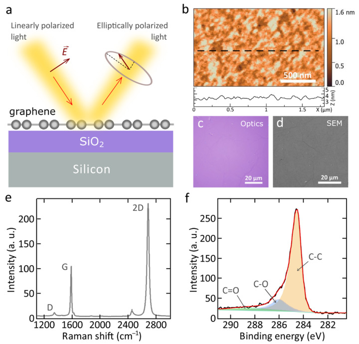
Here, we present the optical properties of commercially available monolayer CVD graphene on glass, quartz, and SiO2/Si substrates. The optical properties were investigated by highly accurate variable-angle spectroscopic ellipsometry (Figure 1a). Before characterization, graphene samples were washed and annealed in a vacuum chamber to remove polymer residuals and water. Ellipsometry data were analyzed and fitted without any additional assumptions such as the presence of water or any other medium on or under the graphene. To ensure the accuracy of our ellipsometric analysis, we utilized optical transmission spectroscopy measurements and X-ray photoelectron spectroscopy (XPS) to analyze the elemental composition and contribution of residues from the transfer process on the graphene samples. All graphene samples were synthesized by the same method and the same manufacturer, so any discrepancies in optical response should not be related to graphene quality differences. For additional analysis, we performed Raman spectroscopy, atomic-force, and scanning electron microscopy to evaluate the quality, thickness, and uniformity of CVD graphene on different substrates.
Figure 1.
(a) The scheme of the ellipsometry measurements. (b) AFM topography mapping of single-layer graphene on SiO2/Si substrate with line profile across the surface. The scan area was 1.8 × 1.1 μm2. (c) Optical image of the graphene on top of SiO2/Si substrate. (d) SEM image of the graphene reveals a high crystallinity of the samples with the crystallite size larger than 10 μm. (e) Raman spectrum of graphene transferred on SiO2/Si substrate, at excitation wavelength λ = 532 nm. (f) Results of XPS fitting analysis of the C1s core level signal obtained for the monolayer graphene on SiO2/Si.
2. Results and Discussion
2.1. Sample Preparation and Characterization
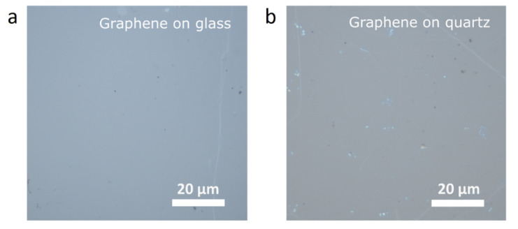
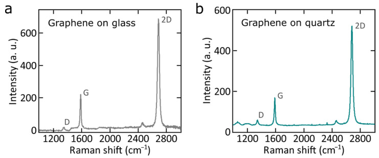
All monolayer graphene films were prepared (see Methods) through chemical vapor deposition. Monolayers of graphene grown initially on copper foil were wet-transferred to three various substrates: SiO2 (285 nm)/Si, fused quartz, and optical glass. Before measurements, graphene samples were washed and annealed in a vacuum chamber to remove polymer residuals and water. The high quality of monolayer graphene films was confirmed by atomic force microscopy (AFM), optical microscopy, and scanning electron microscopy (SEM). The AFM scan image of the graphene on SiO2/Si in Figure 1b confirms a small surface roughness typical for monolayer graphene surfaces. Large-scale optical microscopy images in Figure 1c and Figure A1a,b, and SEM image of the graphene surface in Figure 1d demonstrate that graphene uniformly covers more than 97% of the substrate surface without voids showing good crystallinity of the graphene sample with the crystallite size >10 μm. To characterize the thickness and quality of monolayer graphene on different substrates, we performed Raman spectroscopy measurements (Figure 1e and Figure A2a,b) [36,37]. The ratio of 2D (2689 cm−1) and G (1587 cm−1) bands (>2) indicates the single layer of graphene, and the low intensity of the D band (1347 cm−1), shows its high quality (Figure 1e). Additionally, the 2D band exhibits a sharp Lorentzian peak, specific to a single layer of graphene [38].
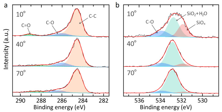
Next, to analyze the presence of residues (from the transfer process) and their contribution to the accuracy of graphene dielectric response characterization, we performed X-ray photoelectron spectroscopy. Figure 1f shows the analysis of the C1s core level constituents for the graphene on SiO2/Si sample, in which the percentage contribution of sp2-graphene, C–O and C=O bonds to C1s are 80.72%, 14.89% and 4.39%, respectively. To investigate the surface composition on top and under the graphene, we made the angle-resolved XPS measurements for the C1s and O1s core level signals in the range of take-off angles from 10° to 70° (measured from the sample surface) that can change the explored depth (see Figure A3) [28]. Both XPS analyses of the C1s and O1s core level signals in Figure A3 demonstrates a small contribution of C–O and C=O bonds, suggesting the negligible residua of polymer on the graphene surface. As the angle decreases, the relative intensity of the C–O, C=O lines in the decomposition of the C1s spectra and O–C lines in the O1s spectra increases. Consequently, these lines are associated with surface states corresponding to adsorbed molecules and polymethylmethacrylate (PMMA) residues. Oxygen anions in SiO2 and H2O share the same binding energy region, and their contributions are indistinguishable. However, from the fact that the relative intensity of the SiO2 + H2O lines in the decomposition of the O1s spectra decreases monotonically with decreasing angle, it can be concluded that H2O does not make a significant contribution to the total intensity of these lines. Indeed, as the angle decreases, photoelectrons are detected from a smaller sample depth. Therefore, the contribution from SiO2 should decrease. If the water concentration in the sample is significant, it partially compensates for the reduced contribution from SiO2. As a result, a nonmonotonic change in the intensity of the SiO2 + H2O line is observed [28]. Noteworthy, the evolution of constituents of the XPS spectra (Figure A3) with the increasing explored depth did not reveal the presence of contamination interlayers (water, PMMA) [28]. Thus they are not considered in the determination of graphene optical constants.
2.2. Dielectric Response Analysis
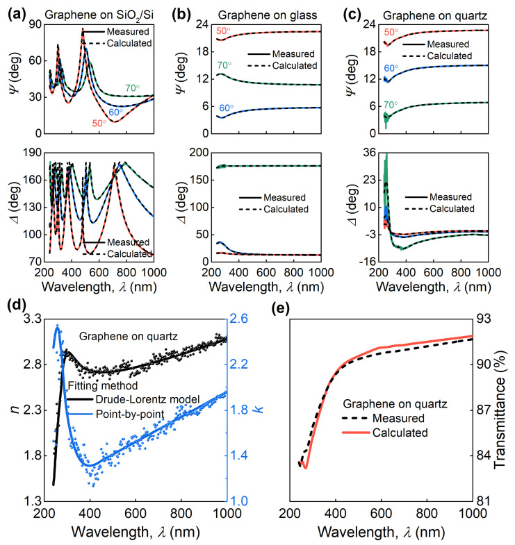
We performed spectroscopic ellipsometry (SE) measurements at multiple incident angles to explore the dielectric response of graphene samples, Figure 2a–c. SE measures the change in light polarization upon reflection from a sample in terms of Ψ and Δ defined through equation tan(Ψ)exp(iΔ) = rp/rs, where rp and rs are sample’s reflection amplitude for p- and s-polarized light. First, we analyzed these Ψ and Δ data by point-by-point inversion to get the initial results presented in Figure 2d. In this approach, optical constants of graphene are varied independently for each wavelength until the best match with the experiment is achieved, allowing to get initial values for the dielectric response of graphene. Then, the dielectric function is fitted by the Drude–Lorentz oscillator model (see Methods and Table 1), which takes into account the optical response of quasi-free electrons (Drude oscillator) and graphene van Hove singularity at π-to-π* interband transition (Lorentz oscillator).Such a fitting approach yields smooth and Kramers–Kronig-consistent dielectric functions compared to noisy point-by-point results (Figure 2d). We calculated the transmittance spectrum based on retrieved optical constants, which is in good agreement with the experimental one as illustrated in Figure 2e, thereby validating the acquired dielectric function.
Figure 2.
Plots of the measured (experiment) and calculated (model) ellipsometric spectra (Ψ and Δ) of monolayer graphene on different substrates: (a) SiO2/Si, (b) glass, and (c) quartz. (d) Refractive index n and extinction coefficient k of monolayer graphene on quartz acquired from SE analysis using different models. (e) Measured (red line) and calculated (black dashed line) transmittance spectra match perfectly within spectrophotometer accuracy (1%).
Table 1.
Drude–Lorentz oscillators parameters for graphene on SiO2/Si, quartz, and glass.
| Substrate | A L | BL (eV) | EL (eV) | ρ (10−4 Ω∙m) | τ (fs) |
|---|---|---|---|---|---|
| SiO2/Si | 8.0531 | 1.5891 | 4.5715 | 5.3668 | 0.60878 |
| Quartz | 8.4404 | 1.6275 | 4.6179 | 4.8038 | 0.65817 |
| Glass | 7.8742 | 1.5650 | 4.5201 | 5.2734 | 0.61750 |
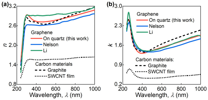
Interestingly, graphene’s optical response is similar in shape to other carbon materials such as graphite [39] and single-walled carbon nanotube (SWCNT) films [40], as illustrated in Figure 3. More importantly, the optical constants of graphene are almost identical to graphite. Consequently, in the considered wavelength range (240–1000 nm), graphene’s optical response is also similar to any number of graphene layers. As a result, the obtained optical constants of graphene could also be used for bilayer, trilayer, and further graphene layers up to graphite. This observation is in total agreement with the results of previous studies [41].
Figure 3.
Comparison of the measured (red lines) refractive index n (a) and extinction coefficient k (b) and some previous results for CVD graphene on glass (blue lines) and quartz (green lines) substrates obtained without any assumptions in the ellipsometric model and carbon materials such as graphite (dashed lines) and SWCNT film (dotted lines). The data of Nelson, Li, Graphite, and SWCNT film are adopted from refs. [26,29,39,40], respectively.
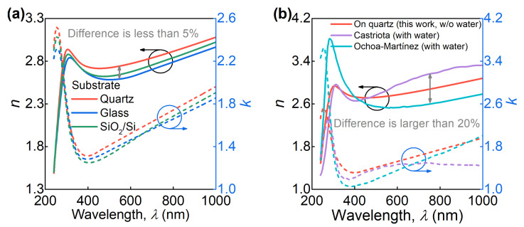
We also investigated graphene transferred on different substrates (quartz, glass, and SiO2/Si) to explore substrate effect, which could explain discrepancies observed in the literature for graphene optical constants. We proceeded with the same procedure as for quartz: first, with the point-by-point approach and the Drude–Lorentz model afterward. The resulting parameters for the Drude–Lorentz model and corresponding optical constants for graphene on quartz, glass, and SiO2/Si substrates are collected in Table 1 and Figure 4a. Clearly, the dielectric function is reproduced with 95% accuracy. Therefore, the substrate effect is negligible for graphene optical constants.
Figure 4.
(a) The measured refractive index n and extinction coefficient k of CVD graphene on three different substrates. For the tabular data, see Appendix A Table A1. (b) Comparison of the measured optical constants (red lines) and some previous results for CVD graphene obtained under the assumption of the presence of nanometer-thick layers of water in the ellipsometric model (cyan and magenta lines). Solid, n, and dashed, k, lines. The data of Ochoa-Martinez and Castriota are adopted from refs. [28,31], respectively.
In contrast, the inclusion of a nanometer-thick water layer in the optical model to consider graphene contamination noticeably changes the result as seen from Figure 4b (there is a large discrepancy by more than 20%). Although this approach allows the inclusion of graphene nonidealities, current devices utilize encapsulated graphene where contamination is minimal. Thus, graphene should be analyzed immediately after the cleaning procedure, as in our work, to enable predictive capabilities for photonic applications.
2.3. Applications
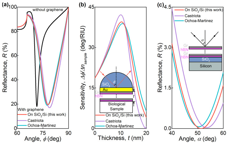
To illustrate the importance of refining the optical constants of graphene, we consider two examples of the devices, including graphene-based heterostructures. One graphene layer could not significantly affect some systems’ optical response because it is too thin, but when several layers of graphene are included in a metamaterial [42,43], the effect of the dielectric function’s inaccuracy becomes apparent. Firstly, we evaluate the optical response of a metamaterial consisting of alternating layers of graphene and h-BN [44], placed on the surface of a standard surface plasmon resonance (SPR) chip, a SiO2 prism with a 40-nm-thick gold film [45]. Such metamaterial enhances the SPR chip’s performance due to the rise of optical sensitivity (Figure 5b) and graphene’s ability to effectively adsorb the studied molecules [12,13]. Figure 5a shows the calculated reflectance of the chip with the optimal (see Figure 5b) 10-nm-thick layer of the metamaterial at a free-space wavelength of 800 nm. Evidently, both the resonance depth and position are strongly dependent on the optical properties of graphene. The expected sensitivity of the considered sensor, shown in Figure 5b, varies by more than 10% when different sources of graphene’s optical properties are used in calculations.
Figure 5.
The operation of the SPR sensor based on SiO2/Au (Au-thickness equals to 40 nm) chip with the metamaterial, consisting of alternating layers graphene and h-BN (a,b). (a) The dependence of the reflection coefficient as a function of the incident angle at the 800 nm wavelength and 10-nm-thick metamaterial. The black curve corresponds to the absence of the metamaterial layer; red, blue, and green curves calculated using different optical properties of graphene, that were reported. (b) The dependence of the sensitivity of this SPR sensor on the thickness of the metamaterial. (c) The TM-mode reflectance from the 20-nm-thick metamaterial, consisting of alternating layers graphene and h-BN, placed on the SiO2/Si substrate (SiO2 thickness equals to 280 nm), as a function of the incident angle at 530 nm free-space wavelength. Red, purple and blue-green curves were calculated using optical properties of graphene from different sources. The optical constants of graphene of Ochoa-Martinez and Castriota are adopted for calculations from refs. [28,31], respectively.
In addition, we consider the same metamaterial (Gr/h-BN) with a 20 nm thickness on top of the standard SiO2/Si substrate to investigate its zero reflection conditions giving rise to phase singularity used in meta-optics design [46]. We evaluate the incident-angle-dependent reflectance of TM-wave at a wavelength of 530 nm using graphene’s optical properties reported by different sources. For optical constants obtained in our work, this structure exhibits zero reflection at an incident angle of approximately 51 degrees, while in the case of the optical constants obtained in [31], the zero reflection angle shifts to 53 degrees. In contrast, for the optical constants obtained in [28], zero reflection is not achieved.
3. Materials and Methods
3.1. Materials
Full area coverage graphene samples were purchased from Graphene Laboratories Inc., Ronkonkoma, NY, USA (https://graphene-supermarket.com accessed on 27 April 2021). Graphene was grown via chemical vapor deposition on a copper foil and wet-transferred onto silicon wafer covered by a 285-nm-thick layer of SiO2, glass (Corning EAGLE XG, New York, NY, USA), and fused quartz (Volume Precision Glass, Inc. G.E. 124, Santa Rosa, CA, USA) substrates. Monolayer graphene covered about 95% of the substrate area. Before measurements, graphene substrates were washed in acetone and isopropyl alcohol baths and annealed at 200 °C in a vacuum chamber 10−6 Torr for more than 1 h to remove residual PMMA and water after the transfer process.
3.2. Raman Characterization
The experimental setup used for Raman measurements was a confocal scanning Raman microscope Horiba LabRAM HR Evolution (HORIBA Ltd., Kyoto, Japan). All measurements were carried out using linearly polarized excitation at wavelength 532 nm, 1800 lines/mm diffraction grating, and × 100 objective (N.A. = 0.90). Meanwhile, we used unpolarized detection to have a significant signal-to-noise ratio. The spot size was ~0.4 µm. The Raman spectra were recorded with 0.9 mW incident powers and an integration time of 10 s at each point. The statistics were collected at least 10 points for each sample.
3.3. XPS Characterization
For the detailed study of the transferred CVD graphene optical response, we carried out the angle-dependent measurements of the O1s and C1s core level XPS spectra to determine contaminants’ presence on top of graphene. Three take-off angles, 10°, 40° and 70° (measured from the surface of the sample), were used to change the explored depth in XPS measurements. In order to investigate the contributions of different bonds, the core-level spectra of the O1s and C1s were decomposed using the XPS peak fitting software package.
3.4. Atomic Force Microscopy, Optical Visualization, Scanning Electron Microscopy
The roughness and homogeneity of the graphene were measured by an atomic force microscope (NT-MDT Ntegra, Moscow, Russia). The surface images (2400 × 2400 pixels) of the graphene samples were captured by an optical microscope (Nikon LV150, Tokyo, Japan) with a digital camera DS-Fi3. To investigate graphene’s surface, we additionally used the scanning electron microscope using the acceleration voltage of 3 kV (JEOL JSM-7001F, Tokyo, Japan).
3.5. Ellipsometry Characterization
Spectroscopic ellipsometry was performed at room temperature at multiple incident angles (50°, 60°, 70°), over a broad spectral range from 240 to 1000 nm (1.24–5.17 eV). The measurements were done using a variable-angle spectroscopic ellipsometer (VASE, J.A. Woollam Co., Lincoln, NE, USA). To avoid any crushes or large tears of graphene, we measured samples in different areas, excluding from consideration the areas close to the edges where graphene’s substrate coverage is minimal. For ellipsometry analysis we implemented the Drude–Lorentz model [47]:
where ε0 is the vacuum dielectric constant, ħ is Planck’s constant, ρ is the resistivity, τ is the mean scattering time, and AL, BL, and EL are the amplitude, the linewidth, and the resonance energy of the Lorentz oscillator.
4. Conclusions
To summarize, we have presented a UV-visible-near-IR (240–1000 nm) spectroscopic ellipsometry of graphene grown by chemical vapor deposition and transferred onto glass, quartz, and SiO2/Si substrates. To obtain an accurate dielectric function suitable for engineering purposes, we thoroughly cleaned and annealed our samples prior to measurements and carried out XPS analysis confirming an ultra-low level of contamination on the graphene’s surface. As a result, we achieved good convergence using a simple ellipsometric model comprising layers of substrate and graphene layer, without auxiliary layers, which are typically introduced to account for residual water and PMMA. The accuracy of the measured optical response was further confirmed by transmittance measurements, which demonstrate remarkable agreement with calculations based on the measured optical constants. Notably, our optical constants show less than 5% variation with changes of the substrate and are very similar to those of graphite, which implies that the measured optical constants are applicable to multilayer graphene structures as well. From a broader perspective, our work provides accurate and universal graphene optical response for the design of photonic devices.
Acknowledgments
The authors thank the MIPT’s Shared Research Facilities Center for the use of their equipment.
Appendix A
Figure A1.
Optical images of the graphene on top of the glass (a) and quartz (b) substrates.
Figure A2.
Raman spectra of graphene transferred on glass (a) and quartz (b) substrates, obtained with an excitation wavelength of λ = 532 nm.
Figure A3.
Results of the angle-resolved XPS measurements of the graphene transferred onto SiO2/Si substrate. Decomposition of C1s (a) and O1s (b) core level signals into their constituents. Take-off angle (measured from the sample surface) increases from 10° to 70°; correspondingly, the explored depth of the sample is increased.
Table A1.
Tabulated optical constants for graphene on different substrates.
| λ (nm) | Substrate | |||||
|---|---|---|---|---|---|---|
| SiO2/Si | Quartz | Glass | ||||
| n | k | n | k | n | k | |
| 240 | 1.5018 | 2.3036 | 1.4913 | 2.3303 | 1.5033 | 2.2261 |
| 260 | 2.1096 | 2.4266 | 2.1676 | 2.5087 | 2.0678 | 2.3145 |
| 280 | 2.6262 | 2.1543 | 2.7044 | 2.1765 | 2.5344 | 2.1402 |
| 300 | 2.866 | 1.7567 | 2.9296 | 1.7667 | 2.7947 | 1.8313 |
| 320 | 2.8629 | 1.496 | 2.9093 | 1.5577 | 2.8391 | 1.5565 |
| 340 | 2.8004 | 1.3584 | 2.8452 | 1.4296 | 2.7962 | 1.389 |
| 360 | 2.7408 | 1.2902 | 2.7901 | 1.3557 | 2.7397 | 1.3133 |
| 380 | 2.6956 | 1.2595 | 2.7539 | 1.3209 | 2.6909 | 1.2874 |
| 400 | 2.6637 | 1.2498 | 2.7338 | 1.3126 | 2.6531 | 1.2834 |
| 420 | 2.6426 | 1.2529 | 2.7222 | 1.3219 | 2.6255 | 1.2907 |
| 440 | 2.6298 | 1.2639 | 2.7167 | 1.343 | 2.6063 | 1.3044 |
| 460 | 2.6234 | 1.28 | 2.7158 | 1.3683 | 2.5938 | 1.3216 |
| 480 | 2.6221 | 1.2997 | 2.7182 | 1.3905 | 2.5864 | 1.3408 |
| 500 | 2.6247 | 1.3216 | 2.7232 | 1.4125 | 2.5838 | 1.3609 |
| 520 | 2.6305 | 1.3451 | 2.7301 | 1.4345 | 2.5849 | 1.3815 |
| 540 | 2.6389 | 1.3697 | 2.7386 | 1.4565 | 2.5888 | 1.4022 |
| 560 | 2.6493 | 1.395 | 2.7483 | 1.4785 | 2.5952 | 1.4228 |
| 580 | 2.6614 | 1.4207 | 2.7591 | 1.5006 | 2.6044 | 1.4433 |
| 600 | 2.6749 | 1.4465 | 2.7708 | 1.5226 | 2.6167 | 1.4635 |
| 620 | 2.6894 | 1.4725 | 2.7832 | 1.5446 | 2.6316 | 1.4836 |
| 640 | 2.7049 | 1.4984 | 2.7962 | 1.5666 | 2.6485 | 1.5035 |
| 660 | 2.721 | 1.5243 | 2.8098 | 1.5886 | 2.6663 | 1.5233 |
| 680 | 2.7376 | 1.55 | 2.8238 | 1.6107 | 2.6843 | 1.5429 |
| 700 | 2.7546 | 1.5756 | 2.8382 | 1.6327 | 2.7021 | 1.5624 |
| 720 | 2.7719 | 1.5976 | 2.8529 | 1.6547 | 2.7196 | 1.5819 |
| 740 | 2.7893 | 1.6196 | 2.868 | 1.6767 | 2.7372 | 1.6013 |
| 760 | 2.8067 | 1.6416 | 2.8834 | 1.6988 | 2.7547 | 1.6206 |
| 780 | 2.824 | 1.6637 | 2.899 | 1.7208 | 2.7723 | 1.64 |
| 800 | 2.8411 | 1.6857 | 2.9148 | 1.7428 | 2.7898 | 1.6593 |
| 820 | 2.8576 | 1.7077 | 2.9307 | 1.7648 | 2.8074 | 1.6786 |
| 840 | 2.8754 | 1.7297 | 2.9469 | 1.7868 | 2.825 | 1.698 |
| 860 | 2.8933 | 1.7518 | 2.9632 | 1.8089 | 2.8425 | 1.7174 |
| 880 | 2.9115 | 1.7738 | 2.9796 | 1.8309 | 2.8601 | 1.7368 |
| 900 | 2.9298 | 1.7958 | 2.9962 | 1.8529 | 2.8776 | 1.7563 |
| 920 | 2.9483 | 1.8178 | 3.0128 | 1.8749 | 2.8952 | 1.7758 |
| 940 | 2.9669 | 1.8398 | 3.0296 | 1.897 | 2.9128 | 1.7953 |
| 960 | 2.9856 | 1.8619 | 3.0464 | 1.919 | 2.9303 | 1.8151 |
| 980 | 3.0044 | 1.8839 | 3.0633 | 1.9412 | 2.9479 | 1.8356 |
| 1000 | 3.0233 | 1.9059 | 3.0803 | 1.9623 | 2.9655 | 1.8571 |
Author Contributions
M.A.E.-S., G.A.E., K.V.V., G.I.T., S.M.N., A.A.V. (Andrey A. Vyshnevyy), A.V.A. and V.S.V. proposed the concept, conceived and designed the experiments and wrote original draft. M.A.E.-S., G.A.E., R.I.R., G.I.T., D.I.Y., N.V.D., A.B.N., V.R.S., A.A.V. (Artem A. Voronov), S.M.N. and A.M.M. performed the measurements and analyzed the data. K.V.V. and A.A.V. (Andrey A. Vyshnevyy) provided theoretical support. All authors discussed the results and contributed to manuscript preparation. M.A.E.-S. and G.A.E. contributed equally to this work and should be considered co-first authors. All authors have read and agreed to the published version of the manuscript.
Funding
The experimental work was supported by the Russian Science Foundation, grant No. 19-79-00350. The numerical analysis of multilayer structures was supported by the Russian Science Foundation, grant No. 20-79-00349.
Institutional Review Board Statement
Not applicable.
Informed Consent Statement
Not applicable.
Data Availability Statement
The data presented in this study are available on request from the corresponding author.
Conflicts of Interest
The authors declare no conflict of interest.
Footnotes
Publisher’s Note: MDPI stays neutral with regard to jurisdictional claims in published maps and institutional affiliations.
References
- 1.Bonaccorso F., Sun Z., Hasan T., Ferrari A.C. Graphene photonics and optoelectronics. Nat. Photonics. 2010;4:611–622. doi: 10.1038/nphoton.2010.186. [DOI] [Google Scholar]
- 2.Bao Q., Loh K.P. Graphene photonics, plasmonics, and broadband optoelectronic devices. ACS Nano. 2012;6:3677–3694. doi: 10.1021/nn300989g. [DOI] [PubMed] [Google Scholar]
- 3.Vakil A., Engheta N. Transformation optics using graphene. Science. 2011;332:1291–1294. doi: 10.1126/science.1202691. [DOI] [PubMed] [Google Scholar]
- 4.Ferrari A.C., Bonaccorso F., Fal’Ko V., Novoselov K.S., Roche S., Bøggild P., Borini S., Koppens F.H.L., Palermo V., Pugno N., et al. Science and technology roadmap for graphene, related two-dimensional crystals, and hybrid systems. Nanoscale. 2015;7:4598–4810. doi: 10.1039/C4NR01600A. [DOI] [PubMed] [Google Scholar]
- 5.Grigorenko A.N., Polini M., Novoselov K.S. Graphene plasmonics. Nat. Photonics. 2012;6:749–758. doi: 10.1038/nphoton.2012.262. [DOI] [Google Scholar]
- 6.Luongo G., Di Bartolomeo A., Giubileo F., Chavarin C.A., Wenger C. Electronic properties of graphene/p-silicon Schottky junction. J. Phys. D Appl. Phys. 2018;51:255305. doi: 10.1088/1361-6463/aac562. [DOI] [Google Scholar]
- 7.Luongo G., Grillo A., Giubileo F., Iemmo L., Lukosius M., Alvarado Chavarin C., Wenger C., Di Bartolomeo A. Graphene Schottky junction on pillar patterned silicon substrate. Nanomaterials. 2018;9:659. doi: 10.3390/nano9050659. [DOI] [PMC free article] [PubMed] [Google Scholar]
- 8.Liu M., Yin X., Ulin-Avila E., Geng B., Zentgraf T., Ju L., Wang F., Zhang X. A graphene-based broadband optical mod-ulator. Nature. 2011;474:64–67. doi: 10.1038/nature10067. [DOI] [PubMed] [Google Scholar]
- 9.Sun Z., Martinez A., Wang F. Optical modulators with 2D layered materials. Nat. Photonics. 2016;10:227–238. doi: 10.1038/nphoton.2016.15. [DOI] [Google Scholar]
- 10.Dalir H., Xia Y., Wang Y., Zhang X. Athermal broadband graphene optical modulator with 35 GHz speed. ACS Photonics. 2016;3:1564–1568. doi: 10.1021/acsphotonics.6b00398. [DOI] [Google Scholar]
- 11.Gan X., Shiue R.-J., Gao Y., Meric I., Heinz T.F., Shepard K.L., Hone J., Assefa S., Englund D. Chip-integrated ultrafast graphene photodetector with high responsivity. Nat. Photonics. 2013;7:883–887. doi: 10.1038/nphoton.2013.253. [DOI] [Google Scholar]
- 12.Wu L., Chu H.S., Koh W.S., Li E.P. Highly sensitive graphene biosensors based on surface plasmon resonance. Opt. Express. 2010;18:14395–14400. doi: 10.1364/OE.18.014395. [DOI] [PubMed] [Google Scholar]
- 13.Stebunov Y.V., Aftenieva O.A., Arsenin A.V., Volkov V.S. Highly sensitive and selective sensor chips with graphene-oxide linking layer. ACS Appl. Mater. Interfaces. 2015;7:21727–21734. doi: 10.1021/acsami.5b04427. [DOI] [PubMed] [Google Scholar]
- 14.Li X., Zhu H., Wang K., Cao A., Wei J., Li C., Jia Y., Li Z., Li X., Wu D. Graphene-on-silicon schottky junction solar cells. Adv. Mater. 2010;22:2743–2748. doi: 10.1002/adma.200904383. [DOI] [PubMed] [Google Scholar]
- 15.Lang F., Gluba M.A., Albrecht S., Rappich J., Korte L., Rech B., Nickel N.H. Perovskite solar cells with large-area cvd-graphene for tandem solar cells. J. Phys. Chem. Lett. 2015;6:2745–2750. doi: 10.1021/acs.jpclett.5b01177. [DOI] [PubMed] [Google Scholar]
- 16.Ermolaev G.A., Stebunov Y.V., Vyshnevyy A.A., Tatarkin D.E., Yakubovsky D.I., Novikov S.M., Baranov D.G., Shegai T., Nikitin A.Y., Arsenin A.V., et al. Broadband optical properties of monolayer and bulk MoS2. NPJ 2D Mater. Appl. 2020;4:1–6. doi: 10.1038/s41699-020-0155-x. [DOI] [Google Scholar]
- 17.Ermolaev G.A., Yakubovsky D.I., Stebunov Y.V., Arsenin A.V., Volkov V.S. Spectral ellipsometry of monolayer transition metal dichalcogenides: Analysis of excitonic peaks in dispersion. J. Vac. Sci. Technol. B. 2020;38:014002. doi: 10.1116/1.5122683. [DOI] [Google Scholar]
- 18.Kravets V.G., Grigorenko A.N., Nair R.R., Blake P., Anissimova S., Novoselov K.S., Geim A.K. Spectroscopic ellipsometry of graphene and an exciton-shifted van Hove peak in absorption. Phys. Rev. B. 2010;81:155413. doi: 10.1103/PhysRevB.81.155413. [DOI] [Google Scholar]
- 19.Matković A., Ralević U., Chhikara M., JakovljeviĆ M.M., Jovanović D., Bratina G., Gajić R. Influence of transfer residue on the optical properties of chemical vapor deposited graphene investigated through spectroscopic ellipsometry. J. Appl. Phys. 2013;114:093505. doi: 10.1063/1.4819967. [DOI] [Google Scholar]
- 20.Wurstbauer U., Röling C., Wurstbauer U., Wegscheider W., Vaupel M., Thiesen P.H., Weiss D. Imaging ellipsometry of graphene. Appl. Phys. Lett. 2010;97:231901. doi: 10.1063/1.3524226. [DOI] [Google Scholar]
- 21.Matković A., Beltaos A., Milićević M., Ralević U., Vasić B., Jovanović D., Gajić R. Spectroscopic imaging ellipsometry and Fano resonance modeling of graphene. J. Appl. Phys. 2012;112:123523. doi: 10.1063/1.4771875. [DOI] [Google Scholar]
- 22.Weber J.J.-W., Calado V.E., Van De Sanden M.R. Optical constants of graphene measured by spectroscopic ellipsometry. Appl. Phys. Lett. 2010;97:091904. doi: 10.1063/1.3475393. [DOI] [Google Scholar]
- 23.Nelson F., Sandin A., Dougherty D.B., Aspnes D.E., Rowe J.E., Diebold A.C. Optical and structural characterization of epitaxial graphene on vicinal 6H-SiC(0001)–Si by spectroscopic ellipsometry, Auger spectroscopy, and STM. J. Vac. Sci. Technol. B. 2012;30:04E106. doi: 10.1116/1.4726199. [DOI] [Google Scholar]
- 24.Boosalis A., Hofmann T., Darakchieva V., Yakimova R., Schubert M. Visible to vacuum ultraviolet dielectric functions of epitaxial graphene on 3C and 4H SiC polytypes determined by spectroscopic ellipsometry. Appl. Phys. Lett. 2012;101:011912. doi: 10.1063/1.4732159. [DOI] [Google Scholar]
- 25.Darakchieva V., Boosalis A., Zakharov A.A., Hofmann T., Schubert M., Tiwald T.E., Iakimov T., Vasiliauskas R., Ya-kimova R. Large-area microfocal spectroscopic ellipsometry mapping of thickness and electronic properties of epitaxial graphene on Si- and C-face of 3C-SiC(111) Appl. Phys. Lett. 2013;102:213116. doi: 10.1063/1.4808379. [DOI] [Google Scholar]
- 26.Nelson F.J., Kamineni V.K., Zhang T., Comfort E.S., Lee J.U., Diebold A.C. Optical properties of large-area polycrystalline chemical vapor deposited graphene by spectroscopic ellipsometry. Appl. Phys. Lett. 2010;97:253110. doi: 10.1063/1.3525940. [DOI] [Google Scholar]
- 27.Chang Y.-C., Liu C.-H., Liu C.-H., Zhong Z., Norris T.B. Extracting the complex optical conductivity of mono- and bilayer graphene by ellipsometry. Appl. Phys. Lett. 2014;104:261909. doi: 10.1063/1.4887364. [DOI] [Google Scholar]
- 28.Ochoa-Martínez E., Gabás M., Barrutia L., Pesquera A., Centeno A., Palanco S., Zurutuza A., Algora C. Determination of a refractive index and an extinction coefficient of standard production of CVD-graphene. Nanoscale. 2015;7:1491–1500. doi: 10.1039/C4NR06119E. [DOI] [PubMed] [Google Scholar]
- 29.Li W., Cheng G., Liang Y., Tian B., Liang X., Peng L., Hight Walker A.R., Gundlach D.J., Nguyen N.V. Broadband optical properties of graphene by spectroscopic ellipsometry. Carbon. 2016;99:348–353. doi: 10.1016/j.carbon.2015.12.007. [DOI] [Google Scholar]
- 30.Song B., Gu H., Zhu S., Jiang H., Chen X., Zhang C., Liu S. Broadband optical properties of graphene and HOPG investigated by spectroscopic Mueller matrix ellipsometry. Appl. Surf. Sci. 2018;439:1079–1087. doi: 10.1016/j.apsusc.2018.01.051. [DOI] [Google Scholar]
- 31.Castriota M., Politano G.G., Vena C., De Santo M.P., Desiderio G., Davoli M., Cazzanelli E., Versace C. Variable angle spectroscopic ellipsometry investigation of CVD-grown monolayer graphene. Appl. Surf. Sci. 2019;467–468:213–220. doi: 10.1016/j.apsusc.2018.10.161. [DOI] [Google Scholar]
- 32.Matković A., Chhikara M., Milićević M., Ralević U., Vasić B., Jovanović D., Belic M.R., Bratina G., Gajic R. Influence of a gold substrate on the optical properties of graphene. J. Appl. Phys. 2015;117:015305. doi: 10.1063/1.4905242. [DOI] [Google Scholar]
- 33.Lin Y.-C., Lu C.-C., Yeh C.-H., Jin C., Suenaga K., Chiu P.-W. Graphene annealing: How clean can it be? Nano Lett. 2012;12:414–419. doi: 10.1021/nl203733r. [DOI] [PubMed] [Google Scholar]
- 34.Lupina G., Kitzmann J., Costina I., Lukosius M., Wenger C., Wolff A., Vaziri S., Östling M., Pasternak I., Krajewska A., et al. Residual Metallic contamination of transferred chemical vapor deposited graphene. ACS Nano. 2015;9:4776–4785. doi: 10.1021/acsnano.5b01261. [DOI] [PubMed] [Google Scholar]
- 35.Yakubovsky D.I., Stebunov Y.V., Kirtaev R.V., Voronin K.V., Voronov A.A., Arsenin A.V., Volkov V.S. Graphene-supported thin metal films for nanophotonics and optoelectronics. Nanomaterials. 2018;8:1058. doi: 10.3390/nano8121058. [DOI] [PMC free article] [PubMed] [Google Scholar]
- 36.Ferrari A.C., Meyer J.C., Scardaci V., Casiraghi C., Lazzeri M., Mauri F., Piscanec S., Jiang D., Novoselov K.S., Roth S., et al. Raman spectrum of graphene and graphene layers. Phys. Rev. Lett. 2006;97:187401. doi: 10.1103/PhysRevLett.97.187401. [DOI] [PubMed] [Google Scholar]
- 37.Albrektsen O., Eriksen R.L., Novikov S.M., Schall D., Karl M., Bozhevolnyi S., Simonsen A.C. High resolution imaging of few-layer graphene. J. Appl. Phys. 2012;111:064305. doi: 10.1063/1.3694660. [DOI] [Google Scholar]
- 38.Graf D., Molitor F., Ensslin K., Stampfer C., Jungen A., Hierold C., Wirtz L. Spatially resolved raman spectroscopy of single- and few-layer graphene. Nano Lett. 2007;7:238–242. doi: 10.1021/nl061702a. [DOI] [PubMed] [Google Scholar]
- 39.Palik E.D. Handbook of Optical Constants of Solids. Elsevier; Amsterdam, The Netherlands: 2012. [Google Scholar]
- 40.Ermolaev G.A., Tsapenko A.P., Volkov V.S., Anisimov A.S., Gladush Y.G., Nasibulin A.G. Express determination of thickness and dielectric function of single-walled carbon nanotube films. Appl. Phys. Lett. 2020;116:231103. doi: 10.1063/5.0012933. [DOI] [Google Scholar]
- 41.Zhu S.-E., Yuan S., Janssen G.C.A. Optical transmittance of multilayer graphene. EPL. 2014;108:17007. doi: 10.1209/0295-5075/108/17007. [DOI] [Google Scholar]
- 42.Chugh S., Man M., Chen Z., Webb K.J. Ultra-dark graphene stack metamaterials. Appl. Phys. Lett. 2015;106:061102. doi: 10.1063/1.4907633. [DOI] [Google Scholar]
- 43.Lin H., Sturmberg B.C.P., Lin K.-T., Yang Y., Zheng X., Chong T.K., De Sterke C.M., Jia B. A 90-nm-thick graphene metamaterial for strong and extremely broadband absorption of unpolarized light. Nat. Photonics. 2019;13:270–276. doi: 10.1038/s41566-019-0389-3. [DOI] [Google Scholar]
- 44.Segura A., Artús L., Cuscó R., Taniguchi T., Cassabois G., Gil B. Natural optical anisotropy of h-BN: Highest giant bire-fringence in a bulk crystal through the mid-infrared to ultraviolet range. Phys. Rev. Mater. 2018;2:024001. doi: 10.1103/PhysRevMaterials.2.024001. [DOI] [Google Scholar]
- 45.Yakubovsky D.I., Arsenin A.V., Stebunov Y.V., Fedyanin D.Y., Volkov V.S. Optical constants and structural properties of thin gold films. Opt. Express. 2017;25:25574–25587. doi: 10.1364/OE.25.025574. [DOI] [PubMed] [Google Scholar]
- 46.Wang Y., Deng Z.-L., Hu D., Yuan J., Ou Q., Qin F., Zhang Y., Ouyang X., Li Y., Peng B., et al. Atomically thin noble metal dichalcogenides for phase-regulated meta-optics. Nano Lett. 2020;20:7811–7818. doi: 10.1021/acs.nanolett.0c01805. [DOI] [PubMed] [Google Scholar]
- 47.Tompkins H.G., Irene E.A. Handbook of Ellipsometry. Springer; Berlin/Heidelberg, Germany: 2005. [Google Scholar]
Associated Data
This section collects any data citations, data availability statements, or supplementary materials included in this article.
Data Availability Statement
The data presented in this study are available on request from the corresponding author.


