

Abstract

To achieve large area growth of transition metal dichalcogenides of uniform monolayer thickness, we demonstrate metal–organic chemical vapor deposition (MOCVD) growth under low pressure followed by a high-temperature sulfurization process under atmospheric pressure (AP). Following sulfurization, the MOCVD-grown continuous MoS2 film transforms into compact triangular crystals of uniform monolayer thickness as confirmed from the sharp distinct photoluminescence peak at 1.8 eV. Raman and X-ray photoelectron spectroscopies confirm that the structural disorders and chalcogen vacancies inherent to the as-grown MOCVD film are substantially healed and carbon/oxygen contaminations are heavily suppressed. The as-grown MOCVD film has a Mo/S ratio of 1:1.6 and an average defect length of ∼1.56 nm, which improve to 1:1.97 and ∼21 nm, respectively, upon sulfurization. The effect of temperature and duration of the sulfurization process on the morphology and stoichiometry of the grown film is investigated in detail. Compared to the APCVD growth, this two-step growth process shows more homogenous distribution of the triangular monolayer MoS2 domains across the entire substrate, while demonstrating comparable electrical performance.
1. Introduction
Molybdenum disulfide (MoS2), belonging to a special family of 2D-layered materials called transition metal dichalcogenides (TMDs), is one of the most thoroughly investigated material due to its unique thickness-dependent electronic and optical properties.1 When thinned down to a monolayer, it develops a direct band gap which makes it suitable for applications such as low-power field-effect transistors (FETs),2 optoelectronics,3,4 and flexible electronics.5 In addition, MoS2 has successfully shown applications in other fields such as memory,6 gas sensors,7 logic circuits,8 spintronics,9 valleytronics,10 and so forth. With such a promise as an emerging candidate for next-generation electronics, it is imperative to have a repeatable, reliable, scalable, and cost-effective synthesis method for uniform large-scale monolayer MoS2. Among various bottom-up synthesis processes, chemical vapor deposition (CVD) has been widely used in growing large area crystalline films with properties comparable to flakes exfoliated mechanically from bulk.11−13 CVD growth of MoS2 is realized by different approaches, the most common one being the molybdenum oxide (MoO3) solid precursor-based CVD under atmospheric pressure (APCVD).14−17 Although full wafer scale growth with grain size as large as hundreds of micrometers can be achieved using the CVD method,11,18 the process suffers severely from several limitations such as overall thickness control, uniformity of grain size/coverage, and repeatability.19,20 Since the powder-based MoO3 precursor has a low vapor pressure, it must be placed in the central heating zone of the furnace which compromises precise control over the ratio of precursor flux, leading to nonuniform thicknesses and inhomogeneity in domain sizes.21 To combat these issues, the use of metal organic precursors having high vapor pressure is being investigated.22 Metal organic CVD (MOCVD) offers more efficient control over the metal flux, and thus, the ratio of metal to chalcogen flux that reaches the substrate can be tailored as required, thereby ensuring uniform thickness control. Several reports have demonstrated MOCVD growth of MoS2 using precursors such as molyhexacarbonyl [Mo(CO)6] for metal and diethyl sulfide [(C2H5)2S] for chalcogen.23−25 Diethyl sulfide inherently leaves considerable carbon residues on the film that degrades material properties.26 Other routes involve creating an air- and moisture-stable precursor tetrakis(diethylaminodithiocarbomato) molybdate(IV) (Mo(Et2NCS2)4) first and then decomposing this single source to form MoS2 via MOCVD.27 Regardless of the precursors used, the growth often results in a polycrystalline film with domain sizes in the order of nanometers.25,28,29 Recently, MOCVD growths of MoS2 with domain sizes larger than 10 μm have been reported. However, they involve long processing times (∼26 h per monolayer)23 or require the substrates to be pre-exposed to halides,25,30 which form the sodium/potassium metal oxide layer below the TMD monolayer, as a byproduct.31 So far, an optimized MOCVD method that yields large-area single-crystal monolayer domains with uniform coverage across the entire substrate and free of contamination, for example, carbon and/or alkali metal oxides, is yet to be developed.
In this work, we report large-area MOCVD growth of the MoS2 film that transforms into homogeneous distribution of single-crystal triangular domains of monolayer thickness by its controlled sulfurization. Several characterization techniques, for example, Raman and photoluminescence (PL) spectroscopies, optical microscopy, scanning electron microscopy (SEM), atomic force microscopy (AFM), and X-ray photoelectron spectroscopy (XPS), are used to determine the crystalline quality, surface morphology, stoichiometry, and contamination level upon sulfurization of the grown films. Following sulfurization, MOCVD-grown MoS2 monolayer domains also show electrical properties that are comparable to those grown by the APCVD method.
2. Experimental Methods
2.1. Material Synthesis
2.1.1. MOCVD Growth of MoS2
Large-area MoS2 was synthesized in an MOCVD growth system under low-pressure conditions [Figure 1a]. The system consists of a quartz tube with an inner diameter of 22 mm (outer diameter = 25 mm) inside a single zone Lindberg/Blue M furnace. The precursors used for MoS2 growth are molybdenum hexacarbonyl, Mo(CO)6 (Sigma-Aldrich, CAS number 13939-06-05, 99.9%), and diethyl sulfide, (C2H5)2S (Sigma-Aldrich, CAS number 352-93-2, 98%). The target substrate used in this work was 285 nm SiO2 grown on highly doped double-side-polished p-type Si. At the start of the growth process, the target substrate (measuring 10 cm × 1.7 cm) was placed approximately 10 cm into the furnace and the system was pumped down to base pressure (∼1.5 mTorr) following which three subsequent purge cycles using ultrahigh purity Ar at 100 sccm were performed. Afterward, Ar flow was cut off and H2 flow was introduced at 5 sccm as the carrier gas for the rest of the growth. Background pressure of the system was held at 5 mTorr. Mo(CO)6 and (C2H5)2S precursors were kept in bubblers in APs at 45 °C and at room temperature, respectively, and the flow rates were controlled via needle valves. The growth was conducted at 850 °C for a duration of 1 min after which the precursor gas flow was cut off and the furnace was allowed to cool down, with only the carrier gas flowing.
Figure 1.

(a) Schematic of the MOCVD growth system. The Raman spectrum of the MoS2 films (b) before and (c) after sulfurization at 850 °C for 30 min. The inset shows the SEM image of a triangular MoS2 domain following sulfurization.
2.1.2. Postgrowth Sulfurization
In another single-zone Lindberg/Blue M CVD furnace, the MOCVD-grown MoS2 sample was loaded in the center with sulfur powder (Sigma-Aldrich, CAS number 7704-34-9, 99.98%) positioned upstream relative to the MoS2 sample and heated separately using a heating coil. The as-grown samples were sulfurized at different temperatures for different durations. The sulfurization procedure was initiated by increasing the temperature of the MoS2 sample to the target temperature. Sulfur was heated to 150 °C, and a carrier gas (N2) was flown in at 10 sccm. After holding the MoS2 film at the target temperature for the desired duration, the furnace heating and the heating coil for sulfur were cut off and subsequently allowed to cool down without any feedback control.
2.1.3. APCVD Growth of MoS2
A clean double-side-polished Si/SiO2 (300 nm, thermally grown oxide) substrate was placed on an alumina combustion boat/crucible containing 8.5 mg of MoO3 (99.5% pure Alfa Aesar, CAS 1313-27-5) and placed inside a 1 in. quartz tube and positioned at the center of a single-zone Lindberg/Blue M furnace.32 A second boat containing S (99.98% Sigma-Aldrich CAS: 7704-34-9) was placed upstream in the tube outside the central heating zone of the furnace, and a separate coil heater was attached to apply heat to the S boat. The system was pumped down to base pressure (∼1.5 mTorr) and purged three times using ultrahigh pure N2 at 200 sccm. The growth was conducted at 850 °C (with S kept at 150 °C) for 5 min under ambient pressure with a carrier gas (N2) flow rate at 10 sccm. The furnace was then turned off, and the lid was opened to let the furnace cool down under ambient conditions.
2.2. Material Characterization
A Veeco tapping-mode AFM instrument was used to image the grown MoS2. Raman and PL spectroscopies were performed on all the samples before and after sulfurization using a Renishaw inVia Raman spectrophotometer system, coupled with 532 nm green laser. Raman and PL spectra were collected using a grating with 3000 lines/mm and 1200 lines/mm, respectively. XPS spectra were recorded using a commercial X-ray photoelectron spectrometer (Kratos Axis Ultra), utilizing a monochromatic Al Kα X-ray source (hυ = 1486.5 eV), electrostatic lens optics, and a multichannel plate and delay line detector coupled to a hemispherical analyzer. The photoelectron takeoff angle was normal to the surface of the sample and 45° with respect to the X-ray beam. High-resolution spectra were collected with a pass energy of 20 eV. The pressure in the XPS chamber was typically 2 × 10⁻⁹ Torr during data acquisition.
2.3. Device Fabrication and Measurement
Uniform monolayer MoS2 domains on Si/SiO2 substrates were identified using a combination of optical contrast, Raman spectroscopy, and AFM. Device active regions and source/drain metal electrodes were defined with electron beam lithography. A stack of Ni/Au (20 nm/30 nm) was deposited as source/drain metal electrodes using an e-beam evaporator. All electrical DC measurements were performed on a Cascade Microtech Summit 11000B-AP probe station using an Agilent 4156C parameter analyzer in ambient at room temperature under dark.
3. Results and Discussions
The experimental setup used for MOCVD growth of MoS2 is schematically shown in Figure 1a. Gas-phase metal–organic precursors molybdenum hexacarbonyl Mo(CO)6 and diethyl sulfide (C2H5)2S are used to grow a thin film of MoS2 under low pressure (∼1.5 mTorr). Growth at 850 °C for 1 min duration results in complete coverage of the Si/SiO2 substrate with a continuous film, as shown in the AFM image [Figure S1]. Raman spectroscopic measurements show two distinct peaks at ∼386 and ∼406 cm–1, which coincide with the Mo–S phonon modes E2g1 (in-plane) and A1g (out-of-plane) peaks of MoS2, respectively, as found in the literature33 [Figure 1b]. However, the asymmetry in the E2g peak suggests the presence of defect-activated peaks and/or peaks due to intermediate oxides that are formed during growth.34 In CVD-grown MoS2, sulfur vacancies are one of the most common defects35,36 which results in unsaturated chemical bond formation between Mo atoms. These bonds can interact with neighboring S atoms and disturb the crystal symmetry which activates phonon modes otherwise unavailable in pristine MoS2. The peak at ∼229 cm–1, referred to as LA(M), possibly originates from the presence of a local maximum in the vibrational density of states located at the energy corresponding to the longitudinal acoustic (LA) branch at the edge of the Brillouin zone.37 Other prominent defect-induced peaks that arise at ∼359, ∼180, and ∼187 cm–1 are assigned to the TO(M), ZA(M), and TA(K) modes, respectively.38 In addition, linewidths of the first-order Raman peaks are wider than those obtained for monolayer MoS2 exfoliated from bulk [Figure S2], thereby corroborating the presence of structural disorders in the grown film.39 These vacancies and disorders can be “repaired” to a great extent by annealing post growth in a S-rich environment. Upon sulfurization at 850 °C under AP for 30 min (more details in the Material Synthesis section), the as-grown film transforms into isolated monolayer triangular domains, as seen in the inset of Figure 1c. During the sulfurization process at high temperature, the carbon impurities from the organic precursors and oxide-based intermediate compounds can be desorbed from the MOCVD-grown film. The incoming S adatoms can react with these unpassivated Mo sites, as well as with the desorbed intermediate compounds in the gas phase, leading to MoS2 triangular domains. Figure 1c shows the Raman spectrum of the MOCVD-grown MoS2 film after sulfurization. Most of the defect-induced peaks present in the as-grown sample disappear following sulfurization and the first-order peak intensities and linewidths are greatly improved [Figure S3], indicating reduction in defect density and improvement in crystalline quality. An additional peak at ∼450 cm–1 now appears after sulfurization due to fewer defects and is attributed to an overlap of two peaks: the second order of the LA mode at the M-point called the 2LA(M) peak and a first-order optical phonon peak A2u.38,40 More detailed Raman spectroscopic analyses for sulfurization at different temperatures and durations are discussed in the later subsections.
To compare our two-step growth process with that of other widely used methods, we have conducted growth of MoS2 via the solid-precursor-based (MoO3 and S powder) APCVD method. Figure 2a shows an optical micrograph of MoS2 grown on the Si/SiO2 substrate. Compact MoS2 domains as large as 40–50 μm are primarily triangular or hexagonal in shape [as shown in the optical and SEM images in Figure 2b,c, respectively]. Figure 2d,e shows Raman and PL spectroscopies of a typical monolayer domain grown by APCVD. The Raman peak difference of ∼19 cm–1 and a sharp distinct PL peak at 1.86 eV [full width at half-maximum (fwhm) is ∼0.06 eV] are consistent with those of monolayer MoS2.33 While this method produces MoS2 with quality comparable to exfoliated flakes, a large portion of the substrate is rendered unusable due to very thick deposits of MoS2, MoO3, and intermediate compounds. The experimental setup used for APCVD growth of MoS2 involves placing the substrate face-down on top of a crucible containing MoO3 powder. Since MoO3 is a low-vapor-pressure solid, it needs to be placed at the center of the heating zone at 850 °C, and hence, the metal precursor flux cannot be precisely controlled. This setup causes majority of the MoO3 powder to evaporate and/or react with S powder either partially or completely depending on local Mo/S ratios. In addition to MoS2 with varying thicknesses, the unreacted and partially reacted MoO3 also deposit on the central region of the substrate, and monolayer MoS2 is formed only in the faint blue region along its periphery [Figure 2a]. Figure 2f shows SEM images from six different points marked on different locations in Figure 2a (color-coded), showing the variation in domain shapes, sizes, distribution, and thicknesses. Domain sizes range from 5 to 100 μm, from the monolayer to bulk in thickness, and the nucleation density decreases as we move downstream. Sharp gradient of concentration of domains across the sample is clearly seen in Figure 2f where the domain density decreases as we move further away from the MoO3 source, indicating a nonhomogeneous coverage. These differences in local Mo/S ratios also give rise to different morphologies, triangles and hexagons, as shown in the inset of Figure 2f.
Figure 2.

APCVD growth of MoS2: (a) optical image of the Si/SiO2 substrate after APCVD growth of MoS2. (b) Optical and (c) SEM images of triangular MoS2 domains. Scale bars are 10 μm. Corresponding Raman and PL spectra are shown in (d,e), respectively. (f) Variation of MoS2 domain size, shape, nucleation density, and thickness in different locations of the sample [color-coded accordingly in (a)]. Scale bars for all the images are 100 μm. Insets show magnified images (scale bars are 25 μm) of one of the domains to signify the domain shape. MOCVD growth of MoS2: (g) optical image of the Si/SiO2 substrate after MOCVD growth of MoS2 followed by sulfurization. (h) Optical and (i) SEM images and the corresponding (j) Raman and (k) PL spectra of triangular MOCVD MoS2 domains. Scale bars are 20 μm for (h) and 10 μm for (i). (l) Uniformity of MoS2 domain size, shape, nucleation density, and thickness in different locations of the sample [color-coded accordingly in (g)]. Scale bars are 100 μm.
Figure 2g shows an optical micrograph of MoS2 grown on the Si/SiO2 substrate via the two-step MOCVD method. Unlike solid-precursor-based APCVD growth, MOCVD uses gas-phase precursors, which results in more uniform film coverage across the substrate. Following the postgrowth sulfurization process at 850 °C for 30 min, mostly isolated triangular MoS2 domains of ∼30 μm in size are formed [as shown in the optical and SEM images in Figure 2h,i, respectively], with a few occurrences of the domains merging to form different types of grain boundaries [as shown in Figure S4], as also observed in MoS2 grown by the APCVD method.41−43 Raman [Figure 2j] and PL [Figure 2k] spectroscopies closely match with that of APCVD-grown MoS2 and the reported literature.41 A slight shift in PL peak position in the case of MOCVD sulfurized domains may be attributed to the strain associated with the high-temperature annealing process. This strain is relaxed upon transfer of the film from the growth substrate.41 SEM images taken from six different spots of the MOCVD film following sulfurization [as marked in Figure 2g] are shown in Figure 2l. Raman spectra from different spots across different MoS2 domains are shown in Figure S5 which does not show any significant variation. These observations confirm that unlike APCVD, this method produces triangular monolayer domains distributed homogeneously across the entire substrate.
To study the effect of annealing conditions, several identical MoS2 samples grown by MOCVD were annealed at different temperatures/durations in a S-rich environment. Figure 3a shows the comparison among normalized Raman spectra of the grown film sulfurized for 30 min at different temperatures: 550, 650, 750, and 850 °C. With the increase in the sulfurization temperature, the distortion in the E2g1 peak which usually arises from the presence of oxide-based intermediate compounds and defects in the MoS2 film gradually transforms into a sharp distinct peak, as expected for pristine single-crystal MoS2. This improvement in crystalline quality is further confirmed from the enhanced peak intensities and reduced linewidths of the first-order Raman peaks. Figure 3b shows variation in peak intensities and the fwhm with increased sulfurization temperature for the A1g Raman peak. As the sulfurization temperature increases, linewidth of the A1g peak decreases from 6.02 to 4.55 cm–1 which indicates gradual reduction in structural disorder44 [Figure 3b]. A similar trend in Raman E2g linewidth with sulfurization temperature is shown in Figure S6. The improvement in crystalline quality is also evident from the enhanced PL peak intensities45 and narrow PL peak width for the sample sulfurized at 850 °C for 30 min, signifying the direct band gap for monolayer MoS2 at 1.8 eV, as shown in Figure 3c. Transformation of the continuous MOCVD-grown MoS2 film into monolayer domains upon sulfurization at various temperatures is shown in Figure S7. Further increase in the sulfurization temperature, however, produces noncompact sparsely populated thicker MoS2, as shown in Figure S8.
Figure 3.

Comparison of Raman and PL spectra of the as-grown MOCVD film following sulfurization at different temperatures and durations. All Raman data have been normalized with respect to Si. (a) Comparison of Raman spectra for the samples sulfurized at different temperatures: 550, 650, 750, and 850 °C. The sulfurization duration was kept 30 min for all the samples. (b) Variation of A1g fwhm and normalized A1g peak intensity with respect to sulfurization temperature. (c) PL spectra for different samples sulfurized at different temperatures. (d) Comparison of the MoS2 Raman peaks as a function of sulfurization duration: as-grown and 5 and 30 min. Sulfurization temperature was kept at 850 °C for all the samples. (e) Variation of A1g fwhm and normalized peak intensity with respect to sulfurization duration. Corresponding variation in PL spectra is shown in (f).
Figure 3d–f shows the Raman and PL spectra of the as-grown MOCVD films compared to samples that were sulfurized at 850 °C for 5 and 30 min. Although optically no significant difference is observed for the duration of 5 min sulfurization, monolayer triangular MoS2 domains appear after 30 min and are distributed uniformly across the substrate (Figure S9). The A1g peak intensity and fwhm also improve accordingly, as shown in Figure 3e. The corresponding PL spectra and gradual improvements in the fwhm are compared in Figures 3f and S10, respectively.
Using diethyl sulfide as the chalcogen precursor in MOCVD growth leaves significant carbon residues in the grown film.23 The Raman spectrum from the as-grown film in Figure 4 (black line) shows the presence of peaks at the defect-related D-band at ∼1347 cm–1 and the graphite-related G band at ∼1597 cm–1,46 confirming the presence of carbonaceous compounds. Similar observation has also been made by Choudhury et al.47 and also by Zhang et al.,48 where the presence of the carbon G peak is observed for the films grown at different temperatures. These peaks disappear completely following sulfurization [Figure 4, blue line], indicating significant reduction in carbon contamination.
Figure 4.

Raman spectra from the MOCVD-grown MoS2 sample showing a prominent graphite-oxide peak (black line) arising from carbon impurities which are suppressed in the sample following sulfurization (blue line).
To further check the film quality and to confirm the presence of oxide and carbon contamination, elemental analysis and chemical stoichiometry quantification were investigated using XPS. Survey spectra from the as-grown and the sulfurized films are shown in the Supporting Information [Figure S11], and all the major peaks are identified. Figure 5 shows high-resolution spectra for Mo-3d, S-2p, and C-1s peaks from the as-grown MOCVD film [Figure 5a] and from samples sulfurized under the optimized conditions [Figure 5b]. The Mo-3d spectra show the clear presence of molybdenum oxide at 236.5 eV on the as-grown film that almost vanishes after sulfurization, indicating conversion of the remaining oxides to MoS2.49 In addition to this, MOCVD film quality suffers greatly due to significant carbon contamination arising from organic precursors such as diethyl sulfide, as mentioned previously [Figure 4]. C-1s spectra from the as-grown film [Figure 5a] can be resolved into the following components: C–C at 284.8 eV, C–O at 286.6 eV, and C=O at 288.8 eV. Upon sulfurization at 850 °C for 30 min, most of the carbon contamination is reduced as seen from a sharp decline in the peak intensity of C-1s spectra in Figure 5b. Some carbon, however, is still present as is the case with all materials that have been exposed to the ambient. The stoichiometry as calculated from the integrated peak areas of Mo and S is found to be Mo/S = 1:1.6 for the as-grown film. This means that about 20% of the sulfur sites are vacancies. If we assume a uniform distribution of the sulfur vacancies, one in every five S-sites has S missing. Considering the distance between adjacent S-sites to be 0.316 nm, the average distance of defects, LD, is found to be ∼1.58 nm. Upon sulfurization, the stoichiometry improves to almost a near ideal value of 1:1.97 which corresponds to an average interdefect distance of ∼21.06 nm. This is a ∼13-fold increase in the average interdefect distance, and it clearly shows the significant improvement in the film quality upon sulfurization. Figure S12 shows the improvement in stoichiometry of MoS2 with increasing sulfurization temperatures. This agrees well with the Raman spectroscopic analyses in Figure 1 where sulfurization helps mitigate the defect-activated Raman modes. In addition, as the defect density decreases, first-order Raman peaks undergo slight shifts, which may arise due to phonon confinement, as seen previously in the case of graphene and other disordered crystals.38 To demonstrate the gradual improvement in the film quality with increasing sulfurization temperature/durations, Figure 6 shows the high-resolution XPS analyses for the samples sulfurized under different conditions. Annealing for 30 min at different temperatures in a S environment and for different durations at 850 °C is shown in Figure 6a,b and 6c,d, respectively. The ratio of MoO3 to MoS2 and the carbon peak intensity gradually decrease with increasing sulfurization temperature [Figures 6b and S13] and duration [Figure 6d], signifying a substantial reduction in defects and oxide/carbon contaminations.
Figure 5.

High-resolution XPS spectra from MoS2 films compared before and after sulfurization: Mo-3d, S-2p, and C-1s peaks from (a) the as-grown and (b) after sulfurization at 850 °C for 30 min.
Figure 6.

(a,b) Comparison of XPS spectra of MoS2 films sulfurized at different temperatures: (a) high-resolution C-1s, Mo-3d, and S-2p peaks and the (b) corresponding variation of C-1s peak intensities and normalized MoO3/MoS2 peak ratios. (c,d) Comparison of XPS spectra of MoS2 sulfurized for different durations: (c) high-resolution C-1s, Mo-3d, and S-2p peaks and the (d) corresponding variation of C-1s peak intensities and normalized MoO3/MoS2 peak ratios.
To test the electrical quality of the film following sulfurization,
back-gated FETs were fabricated on transferred MoS2. Electrical
properties of the as-grown film (Figure S14) show no modulation that could arise due to the presence of defects
in the as-grown film.50 The sulfurized
film was transferred via a poly(methyl methacrylate) (PMMA)-based
wet transfer method using NaOH as the substrate etchant onto the target
Si/SiO2 substrate with alignment mark. Figure 7a shows PL spectra of a MoS2 domain before and after transfer. Shift in the PL peak position
upon transfer indicates relaxation of strain that develops during
the high-temperature growth and annealing cycles.41 Suitable MoS2 domains were identified using
a combination of optical contrast, Raman spectroscopy, and AFM images.
Next, drain/source metal contacts were patterned using e-beam lithography
and, subsequently, contact metals (Ni/Au 20 nm/30 nm) were deposited
using e-beam evaporation followed by liftoff. An optical image of
the final device structure used is shown in the inset of Figure 7b. Electrical measurements
were performed under ambient at room temperature without any illumination. Figure 7b shows the IDS–VGS transfer
characteristics of a SiO2/Si back-gated MoS2 transistor with 285 nm-thick SiO2 being the back-gate
dielectric. The back-gate voltage (VBG) is swept from −30 to 60 V at a drain voltage of 2 V. The
device exhibits a threshold voltage (Vth) of around −10 V. The ON/OFF ratios exceed 106 at a VDS of 2 V with off-state currents
less than 1 pA. Using the slope of the IDS–VGS curve in the linear region,
the field-effect mobility is calculated using 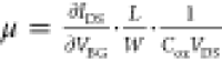 where L, W, and Cox are the channel length, width,
and dielectric capacitance, respectively. Using a value of Cox = 12 nF/cm2 (for 285 nm-thick
SiO2) and L = 500 nm, we obtain a field-effect
mobility value of ∼1 cm2/(V s), which is comparable
to reported values for CVD MoS2 FETs on thermally grown
SiO2.51−53Figure 7c shows the IDS–VDS output curves for back-gate voltages of 20 V to 60
V with an interval of 10 V. From the exponential IDS–VDS at small VDS, it is evident that a Schottky contact is
formed, typical for SiO2/Si back-gated MoS2 FETs.54
where L, W, and Cox are the channel length, width,
and dielectric capacitance, respectively. Using a value of Cox = 12 nF/cm2 (for 285 nm-thick
SiO2) and L = 500 nm, we obtain a field-effect
mobility value of ∼1 cm2/(V s), which is comparable
to reported values for CVD MoS2 FETs on thermally grown
SiO2.51−53Figure 7c shows the IDS–VDS output curves for back-gate voltages of 20 V to 60
V with an interval of 10 V. From the exponential IDS–VDS at small VDS, it is evident that a Schottky contact is
formed, typical for SiO2/Si back-gated MoS2 FETs.54
Figure 7.

(a) Comparison of PL spectra of the sulfurized MoS2 domain before and after a PMMA-based wet transfer. (b) Transfer characteristics for the MoS2-based transistor with a channel length of 500 nm. Optical image of the device is shown in the inset. (c) Output characteristics of the MoS2 transistor in (b).
4. Conclusions
In conclusion, we have grown a continuous MoS2 film via MOCVD and demonstrated its controlled sulfurization to form single-crystal domains with uniform monolayer thickness. The effect of sulfurization temperature and duration is investigated, and an optimized condition is proposed to obtain a homogeneous distribution of large-area single-crystal monolayer domains. The sulfurization process heals sulfur vacancies in the as-grown film, thereby improving the stoichiometry of MoS2, as verified by XPS quantification. Interestingly, carbon contamination, one of the main challenges associated with metal organic precursors, is highly suppressed following sulfurization, as evident from both Raman and XPS analyses. Monolayer nature, high crystallinity, and uniformity of MoS2 domains are confirmed via Raman and PL spectroscopies. Electrical characterization of MoS2 following sulfurization shows performance comparable to that grown by the APCVD method. Our results indicate that this two-step growth method can be considered as a reliable and efficient way to synthesize large-area single-crystal homogeneous domains of MoS2 with uniform monolayer coverage and can also be applied to other sulfur-based TMDs.
Acknowledgments
This work was supported in part by the Army Research Office (ARO) grant #W911NF-17-1-0312 (MURI), NSF NASCENT ERC, and NSF NNCI (carried out at the Texas Nanofabrication Facility at the University of Texas at Austin supported by NSF grant NNCI-1542159). The authors thank Texas Material Instruments scientist Dr. Hugo Celio for aiding in calibration and measurement using XPS.
Supporting Information Available
The Supporting Information is available free of charge at https://pubs.acs.org/doi/10.1021/acsomega.1c00727.
MOCVD growth of the continuous film of MoS2 on the Si/SiO2 substrate; Raman spectra comparison of MOCVD-grown MoS2 and bulk exfoliated MoS2; Raman spectra comparison of MOCVD-grown MoS2 before and after sulfurization; presence of grain boundaries in the sulfurized MOCVD film; homogeneity of the sulfurized MOCVD film; variation of the E2g1 Raman peak with sulfurization temperature; effect of sulfurization temperature on morphology; sulfurization of the as-grown MoS2 film at 950 °C for 30 min; effect of sulfurization duration on morphology; variation of PL fwhm with sulfurization duration; XPS survey scan; improvement of MoS2 stoichiometry with sulfurization temperature; variation of normalized MoO3/MoS2 peak ratios with sulfurization temperature; and electrical properties of back-gated FETs fabricated on the as-grown MOCVD MoS2 (PDF)
Author Present Address
† NOVACentrix, 400 Parker Dr #1110, Austin, Texas 78728, USA.
The authors declare no competing financial interest.
Supplementary Material
References
- Mak K. F.; Lee C.; Hone J.; Shan J.; Heinz T. F. Atomically ThinMoS2: A New Direct-Gap Semiconductor. Phys. Rev. Lett. 2010, 105, 136805. 10.1103/PhysRevLett.105.136805. [DOI] [PubMed] [Google Scholar]
- Bergeron H.; Sangwan V. K.; McMorrow J. J.; Campbell G. P.; Balla I.; Liu X.; Bedzyk M. J.; Marks T. J.; Hersam M. C. Chemical vapor deposition of monolayer MoS2 directly on ultrathin Al2O3 for low-power electronics. Appl. Phys. Lett. 2017, 110, 053101. 10.1063/1.4975064. [DOI] [Google Scholar]
- Chaudhary R.; Patel K.; Sinha R. K.; Kumar S.; Tyagi P. K. Potential application of mono/bi-layer molybdenum disulfide (MoS2) sheet as an efficient transparent conducting electrode in silicon heterojunction solar cells. J. Appl. Phys. 2016, 120, 013104. 10.1063/1.4955071. [DOI] [Google Scholar]
- Mak K. F.; Shan J. Photonics and Optoelectronics of 2D Semiconductor Transition Metal Dichalcogenides. Nat. Photonics 2016, 10, 216–226. 10.1038/nphoton.2015.282. [DOI] [Google Scholar]
- He Q.; Zeng Z.; Yin Z.; Li H.; Wu S.; Huang X.; Zhang H. Fabrication of Flexible MoS2 Thin-Film Transistor Arrays for Practical Gas-Sensing Applications. Small 2012, 8, 2994–2999. 10.1002/smll.201201224. [DOI] [PubMed] [Google Scholar]
- Ge R.; Wu X.; Kim M.; Shi J.; Sonde S.; Tao L.; Zhang Y.; Lee J. C.; Akinwande D. Atomristor: Nonvolatile Resistance Switching in Atomic Sheets of Transition Metal Dichalcogenides. Nano Lett. 2018, 18, 434–441. 10.1021/acs.nanolett.7b04342. [DOI] [PubMed] [Google Scholar]
- Kumar R.; Goel N.; Kumar M. UV-Activated MoS2 Based Fast and Reversible NO2 Sensor at Room Temperature. ACS Sens. 2017, 2, 1744–1752. 10.1021/acssensors.7b00731. [DOI] [PubMed] [Google Scholar]
- Alam M. H.; Xu Z.; Chowdhury S.; Jiang Z.; Taneja D.; Banerjee S. K.; Lai K.; Braga M. H.; Akinwande D. Lithium-Ion Electrolytic Substrates for Sub-1V High-Performance Transition Metal Dichalcogenide Transistors and Amplifiers. Nat. Commun. 2020, 11, 3203. 10.1038/s41467-020-17006-w. [DOI] [PMC free article] [PubMed] [Google Scholar]
- Xu X.; Yao W.; Xiao D.; Heinz T. F. Spin and Pseudospins in Layered Transition Metal Dichalcogenides. Nat. Phys. 2014, 10, 343–350. 10.1038/nphys2942. [DOI] [Google Scholar]
- Xiao D.; Liu G.-B.; Feng W.; Xu X.; Yao W. Coupled Spin and Valley Physics in Monolayers ofMoS2and Other Group-VI Dichalcogenides. Phys. Rev. Lett. 2012, 108, 196802. 10.1103/PhysRevLett.108.196802. [DOI] [PubMed] [Google Scholar]
- Yu H.; Liao M.; Zhao W.; Liu G.; Zhou X. J.; Wei Z.; Xu X.; Liu K.; Hu Z.; Deng K.; Zhou S.; Shi J.-A.; Gu L.; Shen C.; Zhang T.; Du L.; Xie L.; Zhu J.; Chen W.; Yang R.; Shi D.; Zhang G. Wafer-Scale Growth and Transfer of Highly-Oriented Monolayer MoS2 Continuous Films. ACS Nano 2017, 11, 12001–12007. 10.1021/acsnano.7b03819. [DOI] [PubMed] [Google Scholar]
- Lee Y.-H.; Zhang X.-Q.; Zhang W.; Chang M.-T.; Lin C.-T.; Chang K.-D.; Yu Y.-C.; Wang J. T.-W.; Chang C.-S.; Li L.-J.; Lin T.-W. Synthesis of Large-Area MoS2Atomic Layers with Chemical Vapor Deposition. Adv. Mater. 2012, 24, 2320–2325. 10.1002/adma.201104798. [DOI] [PubMed] [Google Scholar]
- Zhang J.; Yu H.; Chen W.; Tian X.; Liu D.; Cheng M.; Xie G.; Yang W.; Yang R.; Bai X.; Shi D.; Zhang G. Scalable Growth of High-Quality Polycrystalline MoS2 Monolayers on SiO2 with Tunable Grain Sizes. ACS Nano 2014, 8, 6024–6030. 10.1021/nn5020819. [DOI] [PubMed] [Google Scholar]
- Xia M.; Li B.; Yin K.; Capellini G.; Niu G.; Gong Y.; Zhou W.; Ajayan P. M.; Xie Y.-H. Spectroscopic Signatures of AA′ and AB Stacking of Chemical Vapor Deposited Bilayer MoS2. ACS Nano 2015, 9, 12246–12254. 10.1021/acsnano.5b05474. [DOI] [PubMed] [Google Scholar]
- Zhou D.; Shu H.; Hu C.; Jiang L.; Liang P.; Chen X. Unveiling the Growth Mechanism of MoS2 with Chemical Vapor Deposition: From Two-Dimensional Planar Nucleation to Self-Seeding Nucleation. Cryst. Growth Des. 2018, 18, 1012–1019. 10.1021/acs.cgd.7b01486. [DOI] [Google Scholar]
- Xu W.; Li S.; Zhou S.; Lee J. K.; Wang S.; Sarwat S. G.; Wang X.; Bhaskaran H.; Pasta M.; Warner J. H. Large Dendritic Monolayer MoS2 Grown by Atmospheric Pressure Chemical Vapor Deposition for Electrocatalysis. ACS Appl. Mater. Interfaces 2018, 10, 4630–4639. 10.1021/acsami.7b14861. [DOI] [PubMed] [Google Scholar]
- Liu K.; Zhang L.; Cao T.; Jin C.; Qiu D.; Zhou Q.; Zettl A.; Yang P.; Louie S. G.; Wang F. Evolution of Interlayer Coupling in Twisted Molybdenum Disulfide Bilayers. Nat. Commun. 2014, 5, 4966. 10.1038/ncomms5966. [DOI] [PubMed] [Google Scholar]
- Lim Y. R.; Song W.; Han J. K.; Lee Y. B.; Kim S. J.; Myung S.; Lee S. S.; An K.-S.; Choi C.-J.; Lim J. Wafer-Scale, Homogeneous MoS2 Layers on Plastic Substrates for Flexible Visible-Light Photodetectors. Adv. Mater. 2016, 28, 5025–5030. 10.1002/adma.201600606. [DOI] [PubMed] [Google Scholar]
- Wang S.; Rong Y.; Fan Y.; Pacios M.; Bhaskaran H.; He K.; Warner J. H. Shape Evolution of Monolayer MoS2 Crystals Grown by Chemical Vapor Deposition. Chem. Mater. 2014, 26, 6371–6379. 10.1021/cm5025662. [DOI] [Google Scholar]
- Özden A.; Ay F.; Sevik C.; Perkgöz N. K. CVD Growth of Monolayer MoS2: Role of Growth Zone Configuration and Precursors Ratio. Jpn. J. Appl. Phys. 2017, 56, 06GG05. 10.7567/JJAP.56.06GG05. [DOI] [Google Scholar]
- Kalanyan B.; Kimes W. A.; Beams R.; Stranick S. J.; Garratt E.; Kalish I.; Davydov A. V.; Kanjolia R. K.; Maslar J. E. Rapid Wafer-Scale Growth of Polycrystalline 2H-MoS2 by Pulsed Metal-Organic Chemical Vapor Deposition. Chem. Mater. 2017, 29, 6279–6288. 10.1021/acs.chemmater.7b01367. [DOI] [PMC free article] [PubMed] [Google Scholar]
- Nguyen T. K.; Nguyen A. D.; Le C. T.; Ullah F.; Koo K.; Kim E.; Kim D.-W.; Jang J. I.; Kim Y. S.. Large-Scale Conformal Growth of Atomic-Thick MoS2 for Highly Efficient Photocurrent Generation, 2018. arXiv:1807.10433v1, 25. [Google Scholar]
- Kang K.; Xie S.; Huang L.; Han Y.; Huang P. Y.; Mak K. F.; Kim C.-J.; Muller D.; Park J. High-Mobility Three-Atom-Thick Semiconducting Films with Wafer-Scale Homogeneity. Nature 2015, 520, 656–660. 10.1038/nature14417. [DOI] [PubMed] [Google Scholar]
- Islam Z.; Zhang K.; Robinson J.; Haque A. Quality enhancement of low temperature metal organic chemical vapor deposited MoS2: an experimental and computational investigation. Nanotechnology 2019, 30, 395402. 10.1088/1361-6528/ab2c3a. [DOI] [PubMed] [Google Scholar]
- Schäfer C. M.; Roque J. C.; Corro E. D.; Bousquet J.; Hébert C.; Sauthier G.; Santiso J.; Garrido J. A.. NaCl-Assisted, Low Pressure MOCVD Growth of Mono- to Few Layer MoS2. 1, Graphene2018 Conference, June 26-29, 2018, Dresden (Germany). [Google Scholar]
- Schäfer C.; Caicedo J. M.; Del Corro E.; Bousquet J.; Hébert C.; Sauthier G.; Garrido J. A.. Assessment of Carbon Contamination in MoS2 Grown by MOCVD Using Mo (CO) 6 and (CH3-CH2) 2S Precursors. Graphene2019 Conference, June 25-28, 2019, Rome (Italy). [Google Scholar]
- McMurtray B.Growth of Molybdenum Disulfide Atomic Layers. 2, NNIN REU Research Accomplishments (2013). [Google Scholar]
- Kim T.; Mun J.; Park H.; Joung D.; Diware M.; Won C.; Park J.; Jeong S.-H.; Kang S.-W. Wafer-scale production of highly uniform two-dimensional MoS2 by metal-organic chemical vapor deposition. Nanotechnology 2017, 28, 18LT01. 10.1088/1361-6528/aa6958. [DOI] [PubMed] [Google Scholar]
- Mun J.; Park H.; Park J.; Joung D.; Lee S.-K.; Leem J.; Myoung J.-M.; Park J.; Jeong S.-H.; Chegal W.; Nam S.; Kang S.-W. High-Mobility MoS2 Directly Grown on Polymer Substrate with Kinetics-Controlled Metal-Organic Chemical Vapor Deposition. ACS Appl. Electron. Mater. 2019, 1, 608–616. 10.1021/acsaelm.9b00078. [DOI] [Google Scholar]
- Kim H.; Ovchinnikov D.; Deiana D.; Unuchek D.; Kis A. Suppressing Nucleation in Metal-Organic Chemical Vapor Deposition of MoS2 Monolayers by Alkali Metal Halides. Nano Lett. 2017, 17, 5056–5063. 10.1021/acs.nanolett.7b02311. [DOI] [PubMed] [Google Scholar]
- Kim H.; Han G. H.; Yun S. J.; Zhao J.; Keum D. H.; Jeong H. Y.; Ly T. H.; Jin Y.; Park J.-H.; Moon B. H.; Kim S.-W.; Lee Y. H. Role of Alkali Metal Promoter in Enhancing Lateral Growth of Monolayer Transition Metal Dichalcogenides. Nanotechnology 2017, 28, 36LT01. 10.1088/1361-6528/aa7e5e. [DOI] [PubMed] [Google Scholar]
- Chowdhury S.; Roy A.; Bodemann I.; Banerjee S. K. Two-Dimensional to Three-Dimensional Growth of Transition Metal Diselenides by Chemical Vapor Deposition: Interplay between Fractal, Dendritic, and Compact Morphologies. ACS Appl. Mater. Interfaces 2020, 12, 15885–15892. 10.1021/acsami.9b23286. [DOI] [PubMed] [Google Scholar]
- Li H.; Zhang Q.; Yap C. C. R.; Tay B. K.; Edwin T. H. T.; Olivier A.; Baillargeat D. From Bulk to Monolayer MoS2: Evolution of Raman Scattering. Adv. Funct. Mater. 2012, 22, 1385–1390. 10.1002/adfm.201102111. [DOI] [Google Scholar]
- Islam M. R.; Kang N.; Bhanu U.; Paudel H. P.; Erementchouk M.; Tetard L.; Leuenberger M. N.; Khondaker S. I. Tuning the Electrical Property via Defect Engineering of Single Layer MoS 2 by Oxygen Plasma. Nanoscale 2014, 6, 10033. 10.1039/C4NR02142H. [DOI] [PubMed] [Google Scholar]
- Förster A.; Gemming S.; Seifert G.; Tománek D. Chemical and Electronic Repair Mechanism of Defects in MoS2 Monolayers. ACS Nano 2017, 11, 9989–9996. 10.1021/acsnano.7b04162. [DOI] [PubMed] [Google Scholar]
- Zhang G.; Wang J.; Wu Z.; Shi R.; Ouyang W.; Amini A.; Chandrashekar B. N.; Wang N.; Cheng C. Shape-Dependent Defect Structures of Monolayer MoS2 Crystals Grown by Chemical Vapor Deposition. ACS Appl. Mater. Interfaces 2017, 9, 763–770. 10.1021/acsami.6b13777. [DOI] [PubMed] [Google Scholar]
- Molina-Sánchez A.; Wirtz L. Phonons in single-layer and few-layer MoS2and WS2. Phys. Rev. B: Condens. Matter Mater. Phys. 2011, 84, 155413. 10.1103/PhysRevB.84.155413. [DOI] [Google Scholar]
- Mignuzzi S.; Pollard A. J.; Bonini N.; Brennan B.; Gilmore I. S.; Pimenta M. A.; Richards D.; Roy D. Effect of disorder on Raman scattering of single-layer MoS2. Phys. Rev. B: Condens. Matter Mater. Phys. 2015, 91, 195411. 10.1103/PhysRevB.91.195411. [DOI] [Google Scholar]
- Shirokura T.; Muneta I.; Kakushima K.; Tsutsui K.; Wakabayashi H. Strong Edge-Induced Ferromagnetism in Sputtered MoS 2 Film Treated by Post-Annealing. Appl. Phys. Lett. 2019, 115, 192404. 10.1063/1.5118913. [DOI] [Google Scholar]
- Frey G. L.; Tenne R.; Matthews M. J.; Dresselhaus M. S.; Dresselhaus G. Raman and Resonance Raman Investigation of MoS 2 Nanoparticles. Phys. Rev. B: Condens. Matter Mater. Phys. 1999, 60, 2883–2892. 10.1103/PhysRevB.60.2883. [DOI] [Google Scholar]
- Roy A.; Ghosh R.; Rai A.; Sanne A.; Kim K.; Movva H. C. P.; Dey R.; Pramanik T.; Chowdhury S.; Tutuc E.; Banerjee S. K. Intra-domain periodic defects in monolayer MoS2. Appl. Phys. Lett. 2017, 110, 201905. 10.1063/1.4983789. [DOI] [Google Scholar]
- Giannazzo F.; Bosi M.; Fabbri F.; Schilirò E.; Greco G.; Roccaforte F. Direct Probing of Grain Boundary Resistance in Chemical Vapor Deposition-Grown Monolayer MoS 2 by Conductive Atomic Force Microscopy. Phys. Status Solidi RRL 2020, 14, 1900393. 10.1002/pssr.201900393. [DOI] [Google Scholar]
- Ly T. H.; Perello D. J.; Zhao J.; Deng Q.; Kim H.; Han G. H.; Chae S. H.; Jeong H. Y.; Lee Y. H. Misorientation-Angle-Dependent Electrical Transport across Molybdenum Disulfide Grain Boundaries. Nat. Commun. 2016, 7, 10426. 10.1038/ncomms10426. [DOI] [PMC free article] [PubMed] [Google Scholar]
- Dumcenco D.; Ovchinnikov D.; Marinov K.; Lazić P.; Gibertini M.; Marzari N.; Sanchez O. L.; Kung Y.-C.; Krasnozhon D.; Chen M.-W.; Bertolazzi S.; Gillet P.; Fontcuberta i Morral A.; Radenovic A.; Kis A. Large-Area Epitaxial Monolayer MoS2. ACS Nano 2015, 9, 4611–4620. 10.1021/acsnano.5b01281. [DOI] [PMC free article] [PubMed] [Google Scholar]
- Wu C.-R.; Liao K.-C.; Wu C.-H.; Lin S.-Y. Luminescence Enhancement and Enlarged Dirac Point Shift of MoS2/Graphene Hetero-Structure Photodetectors With Postgrowth Annealing Treatment. IEEE J. Sel. Top. Quantum Electron. 2017, 23, 101–105. 10.1109/JSTQE.2016.2577519. [DOI] [Google Scholar]
- Kaniyoor A.; Ramaprabhu S. A Raman Spectroscopic Investigation of Graphite Oxide Derived Graphene. AIP Adv. 2012, 2, 032183. 10.1063/1.4756995. [DOI] [Google Scholar]
- Choudhury T. H.; Simchi H.; Boichot R.; Chubarov M.; Mohney S. E.; Redwing J. M. Chalcogen Precursor Effect on Cold-Wall Gas-Source Chemical Vapor Deposition Growth of WS2. Cryst. Growth Des. 2018, 18, 4357–4364. 10.1021/acs.cgd.8b00306. [DOI] [Google Scholar]
- Zhang X.; Al Balushi Z. Y.; Zhang F.; Choudhury T. H.; Eichfeld S. M.; Alem N.; Jackson T. N.; Robinson J. A.; Redwing J. M. Influence of Carbon in Metalorganic Chemical Vapor Deposition of Few-Layer WSe2 Thin Films. J. Electron. Mater. 2016, 45, 6273–6279. 10.1007/s11664-016-5033-0. [DOI] [Google Scholar]
- Murthy A. A.; Li Y.; Palacios E.; Li Q.; Hao S.; DiStefano J. G.; Wolverton C.; Aydin K.; Chen X.; Dravid V. P. Optically Active 1D MoS2 Nanobelts. ACS Appl. Mater. Interfaces 2018, 10, 6799–6804. 10.1021/acsami.7b16892. [DOI] [PubMed] [Google Scholar]
- Okada M.; Okada N.; Chang W.-H.; Endo T.; Ando A.; Shimizu T.; Kubo T.; Miyata Y.; Irisawa T. Gas-Source CVD Growth of Atomic Layered WS2 from WF6 and H2S Precursors with High Grain Size Uniformity. Sci. Rep. 2019, 9, 17678. 10.1038/s41598-019-54049-6. [DOI] [PMC free article] [PubMed] [Google Scholar]
- Amani M.; Chin M. L.; Birdwell A. G.; O’Regan T. P.; Najmaei S.; Liu Z.; Ajayan P. M.; Lou J.; Dubey M. Electrical performance of monolayer MoS2 field-effect transistors prepared by chemical vapor deposition. Appl. Phys. Lett. 2013, 102, 193107. 10.1063/1.4804546. [DOI] [Google Scholar]
- Jeon J.; Jang S. K.; Jeon S. M.; Yoo G.; Jang Y. H.; Park J.-H.; Lee S. Layer-controlled CVD growth of large-area two-dimensional MoS2 films. Nanoscale 2015, 7, 1688–1695. 10.1039/C4NR04532G. [DOI] [PubMed] [Google Scholar]
- Liu B.; Chen L.; Liu G.; Abbas A. N.; Fathi M.; Zhou C. High-Performance Chemical Sensing Using Schottky-Contacted Chemical Vapor Deposition Grown Monolayer MoS2 Transistors. ACS Nano 2014, 8, 5304–5314. 10.1021/nn5015215. [DOI] [PubMed] [Google Scholar]
- Sanne A.; Ghosh R.; Rai A.; Movva H. C. P.; Sharma A.; Rao R.; Mathew L.; Banerjee S. K. Top-gated chemical vapor deposited MoS2 field-effect transistors on Si3N4 substrates. Appl. Phys. Lett. 2015, 106, 062101. 10.1063/1.4907885. [DOI] [Google Scholar]
Associated Data
This section collects any data citations, data availability statements, or supplementary materials included in this article.