

Abstract

Trap states play a crucial role in the design of colloidal quantum dot (QD)-based technologies. The presence of these in-gap states can either significantly limit the efficiency of devices (e.g., in solar cells or LEDs) or play a pivotal role in the functioning of the technology (e.g., in catalysis). Understanding the atomistic nature of traps is therefore of the highest importance. Although the mechanism through which undercoordinated chalcogenide atoms can lead to trap states in II–VI QDs is generally well understood, the nature of metal-based traps remains more elusive. Previous research has shown that reduction of metal sites in negatively charged QDs can lead to in-gap states. Here, we use density functional theory to show that metal-based traps are also formed in charge-neutral but photoexcited CdSe QDs. It is found that Cd–Cd dimers and the concomitant trap states are transient in nature and appear and disappear on the picosecond time scale. Subsequent nonradiative recombination from the trap is shown to be much faster than radiative recombination, indicating that dimer-related trap states can quench the photoluminescence. These results are expected to be transferable to other II–VI materials and highlight the importance of surface redox reactions for the optical properties of QDs. Moreover, they show that photoexcitation can lead to atomic rearrangements on the surface and thus create transient in-gap states.
Introduction
Colloidal quantum dots (QDs) possess unique characteristics like solution processability and size-dependent optical and electronic properties, which make them of particular interest for application in optoelectronic devices.1,2 QD-based technologies have developed quickly over the past few decades,3 leading to the incorporation of QDs in solar cells,4,5 displays,6−8 light-emitting diodes (LEDs),9−11 transistors,12,13 and lasers.14−16 For many of these applications, it is of paramount importance that the band gap remains clear of localized energy levels, as these states can lead to unwanted charge carrier trapping.17,18 Consequently, many methods of removing the influence of trap states have been developed, including the epitaxial growth of an inorganic shell,19,20 the addition of various ligands,21−26 and the electrochemical filling of in-gap states.27−30 However, trap states have also been shown to play an essential role in, for example, optical gain31 or catalytic activity,32 indicating that for certain applications the presence of specific types of traps can be highly advantageous. Thus, a better understanding of the atomistic nature of these trap states may lead not only to more efficient approaches to passivate traps but also to novel strategies aimed at engineering the in-gap states with the desired properties.
Trap states are usually ascribed to the nonbonding orbitals of undercoordinated, often surface-situated atoms.33,34 Density functional theory (DFT) calculations have refined this picture for II–VI semiconductor QDs by showing that in-gap states mainly arise from undercoordinated chalcogenide atoms35 or from reduced metal sites,36 as summarized in Figure 1A. Chalcogenide-based traps (indicated in white in Figure 1A) can be understood in terms of the shape of the orbitals that contribute to the valence band (VB) and conduction band (CB) in II–VI materials. Since the chalcogenide p orbitals mainly constitute the VB, each chalcogenide atom has to be at least 3-fold coordinated to split each of the 3 orthogonal p orbitals. Displacement of Z-type ligands can lead to chalcogenide sites with only two neighboring atoms, causing one of the three p orbitals to remain in the band gap as a nonbonding trap state.35 In contrast, metal atoms mainly contribute to the CB with s orbitals. The spherical symmetry of the s orbital ensures that it is split into bonding and antibonding orbitals, even when the Cd atom is undercoordinated.35 In line with this description, it has been shown experimentally that addition of Z-type ligands, which bind to undercoordinated chalcogenide sites, can indeed increase the photoluminescence quantum yield (PL QY) to near unity.23 Lastly, chalcogenides can also lead to trap states through the formation of chalcogenide dimers upon oxidation (indicated in beige in Figure 1A), as has been shown both experimentally37 and computationally.29,38,39
Figure 1.

Overview of the different traps and trapping mechanisms in CdSe QDs considered in this work. (A) Model of a CdSe QD, showing the surface configurations that can lead to in-gap states. In line with the model system used in this work, the experimentally often employed oleate ligands have been replaced with chloride ions to limit the computational costs of the DFT calculations. Note that the structure shown here is only for illustrative purposes and not the result of a geometry optimization. Two-coordinated Se (2c-Se, white circle) can be formed in charge-balanced QDs,35 while Se–Se dimers (beige oval) may be present in oxidized systems.29,37−39 Cd–Cd dimers (orange oval) can both be formed in negatively doped and charge-neutral but photoexcited QDs (vide infra). Metallic Cd0 (black circle) has so far only been reported for negatively charged QDs36 but is also expected to form upon creation of multiple excitons. (B) Summary of the different steps of trapping an electron in a transient trap state. VB and CB edges are indicated by the black and red horizontal lines, respectively. (i) Excitation of a trap-free QD leads to a CB electron and a VB hole; (ii) presence of this electron in the CB leads to the formation of a trap state that simultaneously traps the electron; (iii) trapped electron recombines with the VB hole; (iv) trap is no longer stabilized by the electron and therefore disappears, leaving the band gap free of in-gap states. (C) Overview of the main recombination pathways in a QD with trapping to a transient surface state: radiative band edge recombination (krad), creation of the trap that captures the electron (ktrap), removal of the trap and simultaneous detrapping of the electron to the CB (kdetrap), and nonradiative decay from the trap to the VB (knonrad).
The existence of metal-based traps is suggested by several experimental studies, which found that both L-type ligands like amines23−25,40 and phosphines24,41 and anionic X-type ligands can increase the PL QY.23,30 These electron-donating ligands cannot passivate undercoordinated chalcogenide atoms and have therefore been proposed to passivate cadmium sites.23,25,30,40 Moreover, spectroelectrochemical studies have found in-gap states near the CB edge of CdSe core-only and core/shell particles, which were ascribed to undercoordinated surface cadmium.42 In our previous computational work,36 it was shown that metal-based traps in II–VI semiconductor QDs can be formed in the presence of excess electrons. It was found that charging trap-free QDs with multiple electrons leads to charge localization on Cd atoms in (111) facets and their subsequent ejection from the lattice (indicated in black in Figure 1A, see also Figure S1 for the different facets in the model QD). If an X-type ligand from the (100) facet is moved to a different position, charging with one excess electron already creates a trap in the form of a Cd–Cd dimer. During the formation of this dimer, which is shown in orange in Figure 1A, the Cd atoms move closer to each other, causing their orbitals to overlap and pushing a bonding Cd–Cd molecular orbital (MO) into the band gap. The injected electron occupies this state, thus stabilizing the Cd–Cd dimer.36
Although the trap formation in charged QDs can be relevant for catalysis32 or QDs in optoelectronic devices,43,44 the question remains how important these metal-based traps are for charge-neutral QDs. The formation of the metal-based traps described in the previous paragraph is essentially a reduction reaction in which electrons in the CB (i.e., with a high electrochemical potential) localize on surface cadmium. It may therefore be possible that also photoexcited electrons can cause the formation of such surface states, leading to a trapping process, in which the trap state itself is formed by the presence of an excited CB electron. Such a trap state would remain in the band gap until the electron recombines with a VB hole or gets detrapped and the transient surface state disappears again, as schematically shown in Figure 1B.
For this type of trap to be relevant for the PL QY, it should form on a time scale comparable to or shorter than the lifetime of the excited state (ES). If trap formation is much slower than that (i.e., ktrap ≪ krad ≈ 108 s–1,45,46 see Figure 1C), it is unlikely for a CB electron to be trapped in a transient surface state. If trapping is much faster than radiative decay (ktrap ≫ krad), two main scenarios are possible. In the first scenario, the nonradiative recombination of the trapped electron to the VB is much slower than the removal of the transient trap (knonrad ≪ kdetrap). Here, the trapping of an electron to a transient surface state does not necessarily reduce the PL QY, but it can lead to long-time tails of PL decay traces47 or result in delayed fluorescence if the detrapping rate is slower than the radiative rate (kdetrap < krad).45 The second scenario arises when the nonradiative recombination is much faster than the detrapping rate (knonrad ≫ kdetrap). Now, nearly every trapped electron will decay nonradiatively to the VB, thus quenching the PL.
Here, we use DFT calculations to investigate both the energetics and the dynamics of Cd–Cd dimers in charge-neutral but photoexcited QDs. Our model QD was constructed in such a way that none of the trap states shown in Figure 1A are present in the ground state (GS). Due to the computational challenges of optimizing singlet ES geometries of large systems, we decided to approximate the ES potential energy surface by a triplet state, as it describes similar orbital features to the lowest singlet ES within the single-particle approximation. This approach ensures that one electron is promoted from the top of the VB to the lowest CB level and makes it possible to carry out ab initio molecular dynamics (AIMD) at limited computational costs. First, geometry optimization will be used to show that given a suboptimal surface passivation, where a chloride ligand has been moved from the (100) to the adjoining (111) facet (see Figure S1), it is energetically favorable for a CB electron to induce Cd–Cd dimer formation, as was previously observed only for negatively charged QDs.36 Next, the time scale on which these dimers form is investigated with AIMD. It is found that when the ligand coverage is already suboptimal, excitation of the QD leads to a Cd–Cd dimer that is both formed and broken up in a period on the order of a picosecond (ktrap, kdetrap ≈ 1012 s–1). Lastly, we draw the configuration coordinate diagrams of the GS and ES for both a trap-free QD and a QD with a Cd–Cd dimer. The nonradiative recombination rate from the trap to the VB (knonrad) is found to be very high, and it is therefore expected that the dynamic formation of Cd–Cd traps can quench the PL QY of photoexcited QDs. These results show that photoexcitation can affect the optical properties of QDs by inducing atomic rearrangements that lead to the creation of transient in-gap states.
Results and Discussion
Model System
For the calculations presented here, a zincblende Cd68Se55Cl26 QD with a diameter of ca. 1.9 nm (see Figure 2A-i) was used as a model system. It is charge balanced as defined by the model of Voznyy et al.48 and contains none of the trap states shown in Figure 1A. It replicates the cation-rich nature of most QDs49,50 but replaces the experimentally often used oleate ligands with computationally less demanding chlorides.51,52 Of the 26 chloride ligands, 24 have been placed on the Cd-terminated (100) facets, as these comprise the Cd atoms with the lowest coordination. The two remaining chlorides have been placed on Cd-terminated (111) facets (see Figure S1 for the different facets of the model QD). This ligand configuration ensures the highest possible coordination of the surface atoms while using a minimum number of ligands (meaning that L-type ligands are not included). During this work, we will therefore refer to this ligand configuration as “perfectly passivated”. Further details of this model system have been discussed previously.35,36 Although we will look at CdSe QDs throughout this work, we expect that the results can be generalized to other zincblende II–VI QDs (vide infra).
Figure 2.

Cd–Cd dimer formation in excited, charge-neutral QDs with imperfect passivation. (A) Structure of the QD when perfectly passivated (left of dashed line) or imperfectly passivated (right of dashed line). Title above each structure indicates whether the respective QD was in the GS or ES. Columns iv and v show that excitation can lead to dimerization between different cadmium atoms. Cd1–Cd2 or Cd3–Cd4 distance, as indicated by the arrows, is given below each structure. For clarity, Cd1 and Cd2 are colored purple and orange, respectively, in panels A-i and A-iv. (B) DOS for each of the QDs. Here, every line corresponds to a MO. Relative contributions of specific atoms or elements to each MO are indicated by the length of the colored line segments. MOs are occupied below the dotted line and empty above it. All ES calculations are unrestricted, meaning that the spin-up (α) and spin-down (β) orbitals are allowed to relax independently (see main text for more details). This results in two distinct densities of states, which are plotted separately on the left and right side of the graph, respectively. (C) Contour plots of the HOMO of each QD at 0.02 e/Bohr3.
Energetics of Dimer Formation
The first step in determining the relevance of Cd–Cd dimer formation for charge-neutral but photoexcited QDs consists of investigating the energetics of the dimerization. If the energy of the QD significantly increases upon dimer formation, the event is unlikely to happen and the trapping rate (ktrap) will be low. Due to the large computational cost of optimizing ES geometries for these systems, we will approximate the photoexcited QD by calculating the GS of the lowest triplet state. This results in a situation where there is a hole in the top of the VB and an electron in the CB edge, thus in a first approximation mimicking the singlet ES. In the ensuing sections, calculations on the QD in its lowest singlet state will therefore be referred to as the GS and calculations on the lowest triplet state as the ES. By extension, “excitation” of a QD indicates its properties are computed for the lowest triplet state.
Figure 2B-i shows the density of states (DOS) of the perfectly passivated model QD in the GS. Here, every horizontal line corresponds to a MO, where the length of each colored line segment indicates the contribution of the corresponding element or atom. The MOs are filled up to the dotted line, indicating that the entire VB is filled with electrons and that the CB is empty. Figure 2B-ii shows the DOS for the perfectly passivated QD in the ES. All of the ES calculations in this work are computed as spin unrestricted, so that the α and β orbitals are allowed to relax independently from each other as a consequence of their different occupation. This approach results in two distinct densities of states: the DOS for the α-electrons is displayed on the left of Figure 2B-ii, while the DOS for β-electrons is given on the right. The dotted lines show that one α electron occupies the CB, whereas the top level of the VB is empty in the β-DOS. The dotted lines thus represent the quasi-Fermi levels of electrons (α electrons, left) and holes (β electrons, right) in the ES. Although the true lowest singlet ES will be a linear combination of different many-electron excitations with the same spin, for the remainder of this work we will approximate the lowest singlet ES by only considering a single electronic transition, i.e., the HOMO-LUMO transition. This approach has been proved to be valid in several works on QDs, in particular, by Prezhdo et al.53 As can be seen by comparing Figure 2A-i and 2A-ii, exciting the QD does not significantly alter its structure. Comparison of Figure 2B and 2C for the perfectly passivated QDs shows that the ES does not lead to new localized in-gap states and that the HOMO remains delocalized over the entire QD. However, note that the shape of the orbitals in Figure 2C changes, since the HOMO is shifted from a VB state consisting mainly of Se 4p orbitals in Figure 2C-i to a CB state consisting mainly of Cd 5s orbitals in Figure 2C-ii.
Figure 2A-iii shows the structure obtained after moving one of the chloride ligands from the (100) to the adjacent (111) facet. Such a surface configuration, which we will refer to as “imperfectly passivated”, may be formed due to random diffusion of ligands over the QD surface, as acetate ligands54 and Z-type complexes55 have been found to be mobile on the QD surface. Since simulating ligand diffusion, which typically occurs on a much longer time scale than that investigated here, is beyond the scope of the current work, the chloride atom was moved to the (111) facet prior to geometry optimization. Moving the chloride to the position shown in Figure 2A-iii increases the energy of the system by roughly 0.47 eV (∼18 kBT) but does not significantly alter the electronic structure (see Figure 2B-iii). The band gap remains free of localized states, and although the HOMO changes in shape, it is still delocalized over the entire QD, as shown in Figure 2C-iii. However, exciting this imperfectly passivated QD reduces the distance between two specific Cd atoms (indicated as Cd1 and Cd2 in Figure 2A-iv) from 3.89 Å for the QD in the GS to 2.93 Å in the ES. At the same time, two in-gap states appear which are ∼30% localized on Cd1 and Cd2. Both of these observations are indicative of the formation of a Cd–Cd dimer.
Figure 2A-v shows that dimerization is not limited to specifically Cd1 and Cd2. The system can also relax to another local minimum that is roughly 0.02 eV (0.9 kBT) higher in energy than the system in Figure 2A-iv and in which a different dimer is obtained. In this case, two Cd atoms at the surface (indicated by Cd3 and Cd4 in Figure 2A-v, see Figure S2 for more details) move closer to each other and form an in-gap state, which is localized ∼40% on those two atoms. The small energy difference between the two systems with the different Cd–Cd dimers indicates that both structures are likely to be sampled under ambient conditions. Indeed, both dimers are found in the AIMD runs discussed in the ensuing section (vide infra).
To summarize, Figure 2 shows that given a suboptimal ligand passivation, the CB electron in photoexcited QDs can energetically lead to the formation of a Cd–Cd dimer and the associated in-gap state. In the Supporting Information we show that CdTe and ZnS QDs exhibit the same dimer formation in the ES (see Figure S3). Therefore, we expect that the traps described in this work can be generalized to zincblende II–VI semiconductor materials in general and potentially also to zincblende III–V QDs, such as InP. As discussed before, whether dimer formation is relevant for excited QDs depends also on the time scale of the dimerization, which will be discussed in the ensuing section.
It must be noted that in real CdSe QDs undercoordinated Cd atoms may not be the only sites that can be reduced by photoexcited electrons. An excited electron may possibly also reduce oxidized selenium sites, like Se–Se dimers or SeOx surface moieties.37,51 Such oxidized selenium sites can be formed by reactions with ambient oxygen or by (unintentional) p-doping (to form Se–Se dimers) and as such represent extrinsic surface effects that were not included in the current calculations, although transient Se–Se dimer formation will be discussed below. In addition, there have been reports on surface Cd reduction and resulting X-type ligand displacement.56 This effect is not seen in the current calculations. However, the free energy change of this reaction will strongly depend on the solvation energy of the displaced X-type ligands, and no solvent is included in our DFT calculations.
Dynamics of Dimer Formation
In this section, AIMD is used to investigate the time scale on which Cd–Cd dimerization occurs. Given the computational costs of AIMD, simulations can only run for a few picoseconds. Therefore, in this section we will assume that random ligand diffusion has already led to the imperfect ligand configuration shown in Figure 2A-iii, and we will investigate how long after excitation the Cd atoms move close enough to each other to form an in-gap state.
As a reference, we first perform an AIMD simulation starting with the GS of the perfectly passivated structure shown in Figure 2A-i (see Methods for further technical details). During the simulation, the DOS is calculated every 20 fs, as shown in Figure 3A-i. At time = 3 ps, the QD is excited, i.e., a triplet is enforced. As discussed in the preceding section for the geometry optimizations, this leads to one α-electron in the CB, while the top of the VB is empty in the β-DOS. Apart from a slight splitting of the α and β levels and a reorganization of the VB levels, no significant changes to the DOS occur. This is corroborated by the contour plots given in Figure 3B-i, which show that the HOMO, at three different times after excitation, remains delocalized over the QD.
Figure 3.

Time-dependent Cd–Cd dimerization in AIMD simulations. (A) DOS as a function of time for (i) a perfectly and (ii) an imperfectly passivated QD. AIMD runs start in the GS but sample the ES after the excitation event at time = 3 ps (see dashed vertical line). Red line in the lower part of the graph shows the distance between Cd1 and Cd2 over time. Blue or gray shaded areas serve as a guide to the eye to indicate the times when a Cd–Cd or Se–Se dimer is present, respectively. (B) Contour plots of the HOMO level at 0.02 e/Bohr3 at time = 1.0, 4.0, 6.0, and 9.0 ps for (i) the perfectly and (ii) the imperfectly passivated QD.
Figure 3A-ii shows the DOS and Cd1–Cd2 distance during an AIMD simulation starting with the GS of the imperfectly passivated QD. During the first 3 ps of the simulation, the DOS shows a clean band gap similar to that of the perfectly passivated QD. Likewise, the average Cd1–Cd2 distance of 3.9 Å is comparable to the value of 4.2 Å found for the perfectly passivated QD. However, when the QD is excited at time = 3 ps, the energy of the lowest α and β CB levels is lowered significantly (see the first blue shaded area) and the Cd1–Cd2 distance decreases to around 3.0 Å. The contour plot of Figure 3B-ii shows that at time = 4.0 ps (i.e., 1.0 ps after excitation), the HOMO is localized on Cd1 and Cd2, indicating that Cd–Cd dimerization has taken place. Around time = 5.3 ps, the in-gap states disappear, accompanied by an increase in the Cd1–Cd2 distance, which then remains stable for approximately 2.2 ps (until time = 7.5 ps). The contour plot shown in Figure 3B-ii at time = 6.0 ps shows that the HOMO has become delocalized during this period, indicating that the Cd–Cd dimer has temporarily been broken up. Around time = 7.5 ps, the Cd1–Cd2 distance decreases again significantly to 3.0 Å and the in-gap state reappears (see the second blue shaded area). This indicates that the Cd–Cd dimer has formed again, as supported by the contour plot at time = 9.0 ps, which shows the localization of the wave function around Cd1 and Cd2. In Figure S4, which shows the same AIMD run extended to ∼21 ps, it can be seen that the Cd1–Cd2 dimer is eventually broken up again, followed by the formation of a dimer between Cd3 and Cd4, similar to the structure found in the geometry optimization in Figure 2-v.
Interesting to note is the VB level that extends far into the band gap at time = 7.0 ps (see the gray shaded area), which we ascribe to an antibonding Se–Se orbital that has also been reported previously.38,57 While in this manuscript we mostly focus on metal-based traps, we note that Se–Se dimer formation appears to be entirely analogous to Cd–Cd dimer formation: oxidation of a QD with undercoordinated Se surface atoms results in Se–Se dimers by depopulating one of the antibonding Se–Se orbitals (see Figure S5),29 analogous to the formation of Cd–Cd dimers upon reduction.36 In addition, photoexcitation can result in transient Cd–Cd dimer formation by electron trapping in the Cd–Cd bonding orbital as well as transient Se–Se dimer formation by hole trapping in the Se–Se antibonding orbital (see Figure S6). Both Cd–Cd dimers and Se–Se dimers lead to trap states in the band gap, formed by the bonding orbital of the Cd–Cd dimer (electron trap) and the antibonding orbital of the Se–Se dimer (hole trap).
From the results presented in this section, we conclude that, upon excitation of an imperfectly passivated QD, the Cd–Cd dimer is formed and broken up again and that both the Cd1–Cd2 and the Cd3–Cd4 dimers are sampled at room temperature. As shown in Figure S4C, the QD is in the dimer configuration for ∼60% of the time, indicating that the rates of trapping and detrapping are roughly equal. As the dimer is formed or broken up every few picoseconds, the (de)trapping rates must hence be on the order of 1 ps–1: ktrap, kdetrap ≈ 1012 s–1. By running the AIMD for a much longer time than the ∼21 ps used here, it would in principle be possible to accurately determine the average lifetime of the Cd–Cd dimer and find more precise values for ktrap and kdetrap. However, this is prohibited by the computational costs of the calculation. Therefore, we will limit our conclusion to stating that both forming and breaking of the Cd–Cd dimers take place on a ∼1 ps time scale (i.e., ktrap, kdetrap ≈ 1012 s–1).
The high rate at which the dimerization takes place suggests that the process occurs with a very small activation energy. To probe the energy of the system as a function of Cd–Cd distance, we carried out constrained geometry optimizations, where the structure is allowed to relax, under the constraint that the coordinates of two selected Cd atoms are frozen to their initial position. First, the structure obtained at time = 3.0 ps in Figure 3A-ii (when no dimer has formed yet) was allowed to relax in the ES while freezing the coordinates of Cd1 and Cd2 so that the Cd1–Cd2 distance remained constant at 4.41 Å. In this way, the most stable configuration at that point without dimer was obtained. Next, the structure around time = 4.0 ps in Figure 3A-ii (when the dimer has just formed) was relaxed in the ES with frozen positions for Cd1 and Cd2 (Cd1–Cd2 distance = 2.87 Å) to obtain the most stable configuration with dimer. The positions of Cd1 and Cd2 were subsequently varied between these two configurations, leading to structures where the Cd1–Cd2 distance ranges from 4.41 to 2.21 Å (structures with a Cd1–Cd2 distances shorter than 2.87 Å were obtained through linear extrapolation). The energy of the relaxed structures (under the aforementioned constraint of freezing the positions of Cd1 and Cd2) are plotted in Figure 4A as a function of Cd1–Cd2 distance (see Figure S7 for the DOS).
Figure 4.

Energy change as a function of Cd–Cd distance. (A) Energy of the QD as a function of the distance between either Cd1 and Cd2 or Cd3 and Cd4 in both the GS (open markers) and the ES (solid markers). Energy of the QD at maximum Cd3–Cd4 separation has been arbitrarily set to zero to facilitate comparison. (B) Contour plots of the HOMO level at 0.02 e/Bohr3 of the QD in the ES at different Cd1–Cd2 distances.
In Figure 4A (black
trace, solid markers), it can be seen that starting from the maximal
Cd1–Cd2 separation in the ES, reducing
the Cd1–Cd2 distance also reduces the
total energy of the system. When the Cd atoms are close enough, the
initially delocalized HOMO level gradually starts to localize on the
Cd–Cd dimer that is being formed (see Figure 4B). After reaching the equilibrium bond length,
further reduction of the Cd1–Cd2 distance
significantly increases the energy again. The data can be described
well with a Morse potential of the form V(r) = De (1 – e–a(r–re))2 – C, as shown by the solid line that is fitted to the data in Figure 4A. Here, De is the depth of the energy well, a determines the width of the well, re is the equilibrium bond length, and C is a constant
that determines the (arbitrary) point of zero potential energy. From
the fit, the dissociation energy of the Cd1–Cd2 dimer (i.e., the depth of the potential energy well De) is estimated to be 0.16 eV (∼6.0 kBT at room temperature), indicating
that the dimer may be broken up by random thermal fluctuations. One
would expect that due to the energetic gain related to dimerization,
the system would spend more time in the dimer state than shown in Figure S4C, where the dimer configuration is
present for only ∼60% of the time. To give a possible explanation
for this, we approximate the QD as a two-level system, where pdimer and pno-dimer are the probability that the QD is in a nuclear
configuration with and without a Cd–Cd dimer, respectively.
Boltzmann statistics state that 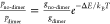 , where
ΔE is the
energy difference between the dimer and no-dimer states and gdimer and gno-dimer are the number of nuclear configurations the
QD can sample in the absence and presence of a Cd–Cd dimer,
respectively (i.e., the degeneracy of each state). This suggests that
there is a higher number of configurations without a dimer, compensating
for the energy gain due to dimerization.
, where
ΔE is the
energy difference between the dimer and no-dimer states and gdimer and gno-dimer are the number of nuclear configurations the
QD can sample in the absence and presence of a Cd–Cd dimer,
respectively (i.e., the degeneracy of each state). This suggests that
there is a higher number of configurations without a dimer, compensating
for the energy gain due to dimerization.
The same trends can
be observed when changing the distance between
two different Cd atoms. Figure 4A (red trace, solid markers) shows the energy changes that
are obtained when varying the distance between Cd3 and
Cd4 (see also Figures S2A-iii/iv) in the ES. Although the exact shape of the curve is different from
the curve obtained for the Cd1–Cd2 dimer
(i.e., the dissociation energy is now 0.17 eV (∼6.7 kBT) and the equilibrium bond
length is 3.1 instead of 3.0 Å), there is no activation energy
required for the formation of the dimer in either case, which is in
agreement with the high rate of dimerization found during the AIMD
simulations. In the absence of an activation barrier, we can estimate
the dimer formation time from the Cd–Cd oscillation frequency.
To this end, we treat the dimer as a harmonic oscillator, of which
the frequency is given by 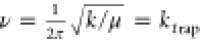 , where k is the spring
constant and μ the reduced mass of the two Cd atoms. To determine
the spring constant, we fit a parabola to the right side of the black
ES curve in Figure 4A (see Figure S8 for details) and obtain k = 0.31 eV/Å2. Using μ = 56.2 u, we find that dimerization occurs in ∼860 fs (ν
= ktrap = 1.2 × 10¹² s–1), which is in good agreement with the AIMD runs.
We note that the Cd–Cd dimerization is a complex process and
that by manually varying the Cd–Cd distance we may not probe
along the exact reaction coordinate. Nevertheless, since we find that
the reaction is barrierless along this suboptimal pathway, it must
be barrierless along the optimal reaction coordinate as well.
, where k is the spring
constant and μ the reduced mass of the two Cd atoms. To determine
the spring constant, we fit a parabola to the right side of the black
ES curve in Figure 4A (see Figure S8 for details) and obtain k = 0.31 eV/Å2. Using μ = 56.2 u, we find that dimerization occurs in ∼860 fs (ν
= ktrap = 1.2 × 10¹² s–1), which is in good agreement with the AIMD runs.
We note that the Cd–Cd dimerization is a complex process and
that by manually varying the Cd–Cd distance we may not probe
along the exact reaction coordinate. Nevertheless, since we find that
the reaction is barrierless along this suboptimal pathway, it must
be barrierless along the optimal reaction coordinate as well.
Figure 4A (black and red traces with open markers) also shows that dimerization is only energetically favorable in the ES. A geometry optimization of the GS, with the same constraints on Cd1/Cd2 or Cd3/Cd4 as imposed previously for the ES, does not lead to an energy well at reduced Cd–Cd distances. Instead, the energy increases with decreasing Cd–Cd distance, in agreement with the geometry optimizations of the preceding section, which showed that dimerization only takes place in the ES.
Nonradiative Recombination from Dimer States
In the preceding section, it was shown that Cd–Cd dimerization takes place on the picosecond time scale and is hence much faster than the radiative lifetime in CdSe QDs (ktrap ≫ krad). In order to decide whether this trapping process also quenches the PL QY, an estimate must be made of the nonradiative recombination rate of the trapped electron and the VB hole (knonrad, see Figure 1C). In this section, we construct the configuration coordinate diagrams for the GS and ES of both the perfectly and the imperfectly passivated QDs. Although it is difficult to extract a quantitative estimate of knonrad from these diagrams, it does provide an intuitive picture on why a Cd–Cd dimer is expected to lead to significantly faster nonradiative decay.
In order to draw the configuration coordinate diagrams, we again
adopt the harmonic approximation and emulate the potential energy
surfaces of the GS and ES by one-dimensional parabolas. In addition,
we approximate the reaction coordinate by the Cd1–Cd2 distance, so that the potential energy of the GS and ES can
be expressed as 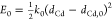 and
and  , respectively. Here, dCd is the Cd1–Cd2 distance,
with dCd,0 and dCd,1 being the Cd1–Cd2 distance at the equilibrium configuration of the GS and ES,
respectively. E is the energy difference between
the minima of the two parabolas, while k0 and k1 refer to the spring constant
of the GS and ES, respectively. Using Nelson’s four-point method,58,59 the parabolas can be drawn by calculating four points along the
potential energy surfaces. First, the energies and Cd1–Cd2 distances at the minima of the parabola were determined by
the geometry optimizations shown in Figure 2A-i-iv. For the vertical transition from
the GS minimum to the ES, a single-point calculation was carried out
in which the triplet state wave function was solved for the nuclear
coordinates at the GS minimum. The vertical transition between the
minimum of the ES and the GS parabola was calculated analogously.
Further details regarding the computational methods are given in the
discussion of Figure S9.
, respectively. Here, dCd is the Cd1–Cd2 distance,
with dCd,0 and dCd,1 being the Cd1–Cd2 distance at the equilibrium configuration of the GS and ES,
respectively. E is the energy difference between
the minima of the two parabolas, while k0 and k1 refer to the spring constant
of the GS and ES, respectively. Using Nelson’s four-point method,58,59 the parabolas can be drawn by calculating four points along the
potential energy surfaces. First, the energies and Cd1–Cd2 distances at the minima of the parabola were determined by
the geometry optimizations shown in Figure 2A-i-iv. For the vertical transition from
the GS minimum to the ES, a single-point calculation was carried out
in which the triplet state wave function was solved for the nuclear
coordinates at the GS minimum. The vertical transition between the
minimum of the ES and the GS parabola was calculated analogously.
Further details regarding the computational methods are given in the
discussion of Figure S9.
Figure 5A compares the configuration coordinate diagrams of a perfectly passivated QD, where the ES remains delocalized over the QD, and an imperfectly passivated QD, where the ES parabola refers to the electron trapped in a Cd–Cd dimer. Comparison of the two figures shows that the bottom of the ES parabola is lower in energy for the imperfectly passivated QD, which is in agreement with the first section of this paper and Figure 4A, where it was shown that the QD can lower its energy in the ES by forming a Cd–Cd dimer. Another difference lies in the horizontal shift of the ES parabola. For the perfectly passivated QD, the parabolas are only slightly shifted, meaning that excitation leads to only minor changes in the Cd1–Cd2 distance, as also shown previously in Figure 2A. In contrast, the large shift of the parabolas in Figure 5A-ii indicates that the Cd1–Cd2 distance reduces significantly upon excitation of the imperfectly passivated QD due to formation of the Cd–Cd dimer. Lastly, the imperfectly passivated QD was created by moving a chloride ligand from the (100) facet (see Figure S1). This causes the QD structure to become less rigid, allowing for the facile formation and dissociation of Cd–Cd dimers that we have seen throughout this work. This is reflected by the shallower shape of the ES parabola in Figure 5A-ii, which indicates that the QD can sample multiple configurations (i.e., Cd–Cd distances) without significantly increasing its energy.
Figure 5.

Estimation of knonrad by constructing configuration coordinate diagrams. (A) Configuration coordinate diagrams for (i) a perfectly passivated QD and (ii) an imperfectly passivated QD with a Cd–Cd dimer in the ES. (B) Schematic overview of the main recombination pathways in a QD with a Cd–Cd dimer.
Due to both the larger displacement and the shallower
potential
well of the ES in the QD with the dimer (see Figure 5A), the activation energy required to nonradiatively
cross from the ES minimum to the GS parabola (Eact = 0.06 eV) is significantly lower than that for the perfectly
passivated QD (Eact = 0.96 eV). From this
decrease in activation energy we can infer an estimate for the acceleration
of the nonradiative decay according to 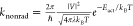 .60−62 Here, V is the
electronic coupling between the GS and the ES, estimated from calculating
the absorption spectrum of the QD in the relaxed ES configuration
within the single-orbital approximation, as implemented in the Nano-QMFlows
package.63 Taking λ as the total
reorganization energy (see Figure S9) yields
the decay rates knonrad,perf ≈
10–1 s–1 and knonrad,imp ≈ 1013 s–1 for the perfectly and imperfectly passivated QD, respectively. While
we stress that these values must be seen as rough estimates only,
due to both the one-dimensional parabolic approximation and the exponential
dependence of the decay rate on the activation barrier, the order-of-magnitude
disparity in both rates undoubtedly shows that dimer formation greatly
accelerates nonradiative decay. Furthermore, the nonradiative decay
from the trap state is also expected to be much faster than radiative
recombination (knonrad,imp > krad ≈ 108 s–1,45,46 as summarized in Figure 5B), indicating that dimer formation efficiently
quenches the
PL. As shown in Figure S10, this result
is robust even when accounting for the known underestimation of the
band gap in DFT/PBE (see Methods).64
.60−62 Here, V is the
electronic coupling between the GS and the ES, estimated from calculating
the absorption spectrum of the QD in the relaxed ES configuration
within the single-orbital approximation, as implemented in the Nano-QMFlows
package.63 Taking λ as the total
reorganization energy (see Figure S9) yields
the decay rates knonrad,perf ≈
10–1 s–1 and knonrad,imp ≈ 1013 s–1 for the perfectly and imperfectly passivated QD, respectively. While
we stress that these values must be seen as rough estimates only,
due to both the one-dimensional parabolic approximation and the exponential
dependence of the decay rate on the activation barrier, the order-of-magnitude
disparity in both rates undoubtedly shows that dimer formation greatly
accelerates nonradiative decay. Furthermore, the nonradiative decay
from the trap state is also expected to be much faster than radiative
recombination (knonrad,imp > krad ≈ 108 s–1,45,46 as summarized in Figure 5B), indicating that dimer formation efficiently
quenches the
PL. As shown in Figure S10, this result
is robust even when accounting for the known underestimation of the
band gap in DFT/PBE (see Methods).64
An interesting question concerns the frequency with which these dimers form in practice. As has just been shown, dimer formation is a very rapid process given imperfect surface passivation. Yet, as discussed at the start of the Results and Discussion, for the current work it was assumed that the surface ligands were already in such a suboptimal configuration. How often these imperfect surface configurations occur will depend on how the ligands diffuse over the surface or possibly desorb from the surface followed by resorption from the solution at a different site. These processes are expected to take place on a much longer time scale than investigated here. Moreover, for a realistic simulation of these processes, in addition to the X-type ligands employed here, L-type ligands and solvent molecules must be taken into account explicitly, as they will significantly influence the way ligands move across the QD surface. Although beyond the scope of the current work, such calculations may give great insight into how often surface configurations appear that allow for Cd–Cd dimer formation and if that time scale agrees with, for example, QD blinking.
Conclusions
In conclusion, DFT calculations have been used to study the formation of Cd–Cd dimers and the concomitant traps in charge-neutral but photoexcited CdSe QDs. We showed that for suboptimal surface passivation, the formation of Cd–Cd dimers is energetically favorable in a photoexcited QD. Ab initio molecular dynamics simulations show that the formation of the trap is a dynamic process and that the in-gap state appears and disappears in a period on the order of 1 ps as a result of a barrierless reaction with a relatively shallow potential well. Lastly, construction of configuration coordinate diagrams shows that nonradiative recombination from the trapped state is much faster than radiative recombination, which leads us to conclude that these transient Cd–Cd dimer traps strongly reduce the PL QY. These results show that photoexcitation can lead to atomic rearrangements and thus create transient in-gap states. Finally, we find that a similar metal-based dimer formation occurs in the excited state of other II–VI semiconductor QDs, suggesting that this type of trap may be important for the reduction of the PL QY in a broad range of semiconductor nanomaterials.
Methods
Geometry optimizations and AIMD simulations have been carried out at the DFT level with a PBE exchange-correlation functional65 and double-ζ basis set, as implemented in the CP2K quantum chemistry software package.66 Relativistic effects have been taken into account through the use of effective core potentials. The ES calculations were performed without spin restrictions. Geometry optimizations were carried out at 0 K in the gas phase. AIMD simulations were performed in the canonical (NVT) ensemble at a constant temperature of 300 K using a velocity rescaling thermostat.67 MD simulations of QDs in the GS were typically run for ≥12 ps, of which the first 2 ps were discarded as an equilibration step. MD runs of the QDs in the ES were restarted from the atomic positions and velocities as obtained from the GS MD simulations. Further details are given in the main text and, for the construction of the configuration coordinate diagrams, in the SI.
Acknowledgments
A.J.H. acknowledges the European Research Council Horizon 2020 ERC Grant Agreement No. 678004 (Doping on Demand) for financial support. I.I. acknowledges support from The Netherlands Organization of Scientific Research (NWO) through the Innovational Research Incentive (Vidi) Scheme (Grant No. 723.013.002). S.C.B. acknowledges financial support through the Innovational Research Incentives (Veni) Scheme (Grant No. 722.017.011). This work was sponsored by NWO Exact and Natural Sciences for the use of supercomputer facilities and was carried out on the Dutch national e-infrastructure with the support of the SURF Cooperative.
Supporting Information Available
The Supporting Information is available free of charge at https://pubs.acs.org/doi/10.1021/acs.chemmater.1c00561.
Indication of the different facets of the model QD; structure and DOS for the Cd3–Cd4 dimer; structure and DOS for CdTe and ZnS QDs with a metal–metal dimer; DOS and Cd–Cd distance for the complete AIMD runs; structure, DOS, and discussion of the Se–Se dimer; DOS as a function of the Cd1–Cd2 distance in the GS and ES; estimation of the dimerization rate from the potential energy landscape; details on the construction of the configuration coordinate diagrams; discussion of the effect of the band gap on the nonradiative decay rate (PDF)
Author Contributions
The manuscript was written through contributions of all authors. All authors have given approval to the final version of the manuscript.
The authors declare no competing financial interest.
Supplementary Material
References
- Talapin D. V.; Lee J.-S.; Kovalenko M. V.; Shevchenko E. V. Prospects of Colloidal Nanocrystals for Electronic and Optoelectronic Applications. Chem. Rev. 2010, 110, 389–458. 10.1021/cr900137k. [DOI] [PubMed] [Google Scholar]
- de Mello Donegá C. Synthesis and properties of colloidal heteronanocrystals. Chem. Soc. Rev. 2011, 40, 1512–1546. 10.1039/C0CS00055H. [DOI] [PubMed] [Google Scholar]
- Litvin A. P.; et al. Colloidal quantum dots for optoelectronics. J. Mater. Chem. A 2017, 5, 13252–13275. 10.1039/C7TA02076G. [DOI] [Google Scholar]
- Carey G. H.; et al. Colloidal Quantum Dot Solar Cells. Chem. Rev. 2015, 115, 12732–12763. 10.1021/acs.chemrev.5b00063. [DOI] [PubMed] [Google Scholar]
- Ganesan A. A.; Houtepen A. J.; Crisp R. W. Quantum Dot Solar Cells: Small Beginnings Have Large Impacts. Appl. Sci. 2018, 8, 1867. 10.3390/app8101867. [DOI] [Google Scholar]
- Jang E.; et al. White-light-emitting diodes with quantum dot color converters for display backlights. Adv. Mater. 2010, 22, 3076–3080. 10.1002/adma.201000525. [DOI] [PubMed] [Google Scholar]
- Kim Y.; et al. Bright and Uniform Green Light Emitting InP/ZnSe/ZnS Quantum Dots for Wide Color Gamut Displays. ACS Appl. Nano Mater. 2019, 2, 1496–1504. 10.1021/acsanm.8b02063. [DOI] [Google Scholar]
- Ziegler J.; et al. Silica-coated InP/ZnS nanocrystals as converter material in white LEDs. Adv. Mater. 2008, 20, 4068–4073. 10.1002/adma.200800724. [DOI] [Google Scholar]
- Shirasaki Y.; Supran G. J.; Bawendi M. G.; Bulović V. Emergence of colloidal quantum-dot light-emitting technologies. Nat. Photonics 2013, 7, 13. 10.1038/nphoton.2012.328. [DOI] [Google Scholar]
- Lim J.; Park Y. S.; Wu K.; Yun H. J.; Klimov V. I. Droop-Free Colloidal Quantum Dot Light-Emitting Diodes. Nano Lett. 2018, 18, 6645–6653. 10.1021/acs.nanolett.8b03457. [DOI] [PubMed] [Google Scholar]
- Kim S.; et al. High-Performance Transparent Quantum Dot Light-Emitting Diode with Patchable Transparent Electrodes. ACS Appl. Mater. Interfaces 2019, 11, 26333–26338. 10.1021/acsami.9b05969. [DOI] [PubMed] [Google Scholar]
- Chung D. S.; et al. Low voltage, hysteresis free, and high mobility transistors from all-inorganic colloidal nanocrystals. Nano Lett. 2012, 12, 1813–1820. 10.1021/nl203949n. [DOI] [PubMed] [Google Scholar]
- Balazs D. M.; et al. Colloidal Quantum Dot Inks for Single-Step-Fabricated Field-Effect Transistors: The Importance of Postdeposition Ligand Removal. ACS Appl. Mater. Interfaces 2018, 10, 5626–5632. 10.1021/acsami.7b16882. [DOI] [PMC free article] [PubMed] [Google Scholar]
- Kovalenko M. V.; et al. Prospects of nanoscience with nanocrystals. ACS Nano 2015, 9, 1012–1057. 10.1021/nn506223h. [DOI] [PubMed] [Google Scholar]
- Geiregat P.; Van Thourhout D.; Hens Z. A bright future for colloidal quantum dot lasers. NPG Asia Mater. 2019, 11, 41. 10.1038/s41427-019-0141-y. [DOI] [Google Scholar]
- Pietryga J. M.; et al. Spectroscopic and Device Aspects of Nanocrystal Quantum Dots. Chem. Rev. 2016, 116, 10513–10622. 10.1021/acs.chemrev.6b00169. [DOI] [PubMed] [Google Scholar]
- Katsiev K.; et al. The Complete In-Gap Electronic Structure of Colloidal Quantum Dot Solids and Its Correlation with Electronic Transport and Photovoltaic Performance. Adv. Mater. 2014, 26, 937–942. 10.1002/adma.201304166. [DOI] [PubMed] [Google Scholar]
- Kagan C. R.; Lifshitz E.; Sargent E. H.; Talapin D. V. Building devices from colloidal quantum dots. Science 2016, 353, aac5523 10.1126/science.aac5523. [DOI] [PubMed] [Google Scholar]
- Reiss P.; Protière M.; Li L. Core/shell semiconductor nanocrystals. Small 2009, 5, 154–168. 10.1002/smll.200800841. [DOI] [PubMed] [Google Scholar]
- Jang Y.; et al. Interface control of electronic and optical properties in IV-VI and II-VI core/shell colloidal quantum dots: a review. Chem. Commun. 2017, 53, 1002–1024. 10.1039/C6CC08742F. [DOI] [PubMed] [Google Scholar]
- Page R. C.; et al. Near-Unity Quantum Yields from Chloride Treated CdTe Colloidal Quantum Dots. Small 2015, 11, 1548–1554. 10.1002/smll.201402264. [DOI] [PMC free article] [PubMed] [Google Scholar]
- Stein J. L.; Mader E. A.; Cossairt B. M. Luminescent InP Quantum Dots with Tunable Emission by Post-Synthetic Modification with Lewis Acids. J. Phys. Chem. Lett. 2016, 7, 1315–1320. 10.1021/acs.jpclett.6b00177. [DOI] [PubMed] [Google Scholar]
- Kirkwood N.; et al. Finding and Fixing Traps in II-VI and III-V Colloidal Quantum Dots: The Importance of Z-type Ligand Passivation. J. Am. Chem. Soc. 2018, 140, 15712–15723. 10.1021/jacs.8b07783. [DOI] [PMC free article] [PubMed] [Google Scholar]
- Shen Y.; Tan R.; Gee M. Y.; Greytak A. B. Quantum Yield Regeneration: Influence of Neutral Ligand Binding on Photophysical Properties in Colloidal Core/Shell Quantum Dots. ACS Nano 2015, 9, 3345–3359. 10.1021/acsnano.5b00671. [DOI] [PubMed] [Google Scholar]
- Gao Y.; Peng X. Photogenerated Excitons in Plain Core CdSe Nanocrystals with Unity Radiative Decay in Single Channel: The Effects of Surface and Ligands. J. Am. Chem. Soc. 2015, 137, 4230–4235. 10.1021/jacs.5b01314. [DOI] [PubMed] [Google Scholar]
- Fan J. Z.; et al. Mixed Lead Halide Passivation of Quantum Dots. Adv. Mater. 2019, 31, 1904304. 10.1002/adma.201904304. [DOI] [PubMed] [Google Scholar]
- Weaver A. L.; Gamelin D. R. Photoluminescence Brightening via Electrochemical Trap Passivation in ZnSe and Mn2+-Doped ZnSe Quantum Dots. J. Am. Chem. Soc. 2012, 134, 6819–6825. 10.1021/ja301102h. [DOI] [PubMed] [Google Scholar]
- Rinehart J. D.; Weaver A. L.; Gamelin D. R. Redox Brightening of Colloidal Semiconductor Nanocrystals Using Molecular Reductants. J. Am. Chem. Soc. 2012, 134, 16175–16177. 10.1021/ja307996b. [DOI] [PubMed] [Google Scholar]
- Boehme S. C.; et al. Density of Trap States and Auger-mediated Electron Trapping in CdTe Quantum-Dot Solids. Nano Lett. 2015, 15, 3056–3066. 10.1021/acs.nanolett.5b00050. [DOI] [PubMed] [Google Scholar]
- van der Stam W.; et al. Spectroelectrochemical Signatures of Surface Trap Passivation on CdTe Nanocrystals. Chem. Mater. 2018, 30, 8052–8061. 10.1021/acs.chemmater.8b03893. [DOI] [PMC free article] [PubMed] [Google Scholar]
- Geiregat P.; et al. Continuous-wave infrared optical gain and amplified spontaneous emission at ultralow threshold by colloidal HgTe quantum dots. Nat. Mater. 2018, 17, 35–42. 10.1038/nmat5000. [DOI] [PubMed] [Google Scholar]
- Zhao J.; Holmes M. A.; Osterloh F. E. Quantum Confinement Controls Photocatalysis: A free Energy Analysis for Photocatalytic Proton Reduction at CdSe Nanocrystals. ACS Nano 2013, 7, 4316–4325. 10.1021/nn400826h. [DOI] [PubMed] [Google Scholar]
- Knowles K. E.; Tice D. B.; McArthur E. A.; Solomon G. C.; Weiss E. A. Chemical Control of the Photoluminescence of CdSe Quantum Dot-Organic Complexes with a Series of Para-Substituted Aniline Ligands. J. Am. Chem. Soc. 2010, 132, 1041–1050. 10.1021/ja907253s. [DOI] [PubMed] [Google Scholar]
- Boles M. A.; Ling D.; Hyeon T.; Talapin D. V. The surface science of nanocrystals. Nat. Mater. 2016, 15, 141–153. 10.1038/nmat4526. [DOI] [PubMed] [Google Scholar]
- Houtepen A. J.; Hens Z.; Owen J. S.; Infante I. On the Origin of Surface Traps in Colloidal II-VI Semiconductor Nanocrystals. Chem. Mater. 2017, 29, 752–761. 10.1021/acs.chemmater.6b04648. [DOI] [Google Scholar]
- du Fossé I.; Ten Brinck S.; Infante I.; Houtepen A. J. Role of Surface Reduction in the Formation of Traps in n-Doped II-VI Semiconductor Nanocrystals: How to Charge without Reducing the Surface. Chem. Mater. 2019, 31, 4575–4583. 10.1021/acs.chemmater.9b01395. [DOI] [PMC free article] [PubMed] [Google Scholar]
- Tsui E. Y.; Hartstein K. H.; Gamelin D. R. Selenium Redox Reactivity on Colloidal CdSe Quantum Dot Surfaces. J. Am. Chem. Soc. 2016, 138, 11105–11108. 10.1021/jacs.6b06548. [DOI] [PMC free article] [PubMed] [Google Scholar]
- Sabatini R. P.; et al. Temperature-Induced Self-Compensating Defect Traps and Gain Thresholds in Colloidal Quantum Dots. ACS Nano 2019, 13, 8970–8976. 10.1021/acsnano.9b02834. [DOI] [PubMed] [Google Scholar]
- Hartley C. L.; Kessler M. L.; Dempsey J. L. Molecular-Level Insight into Semiconductor Nanocrystal Surfaces. J. Am. Chem. Soc. 2021, 143, 1251–1266. 10.1021/jacs.0c10658. [DOI] [PubMed] [Google Scholar]
- Pu C.; Peng X. To Battle Surface Traps on CdSe/CdS Core/Shell Nanocrystals: Shell Isolation versus Surface Treatment. J. Am. Chem. Soc. 2016, 138, 8134–8142. 10.1021/jacs.6b02909. [DOI] [PubMed] [Google Scholar]
- Kalyuzhny G.; Murray R. W. Ligand effects on optical properties of CdSe nanocrystals. J. Phys. Chem. B 2005, 109, 7012–7021. 10.1021/jp045352x. [DOI] [PubMed] [Google Scholar]
- Van Der Stam W.; et al. Electrochemical Modulation of the Photophysics of Surface-Localized Trap States in Core/Shell/(Shell) Quantum Dot Films. Chem. Mater. 2019, 31, 8484–8493. 10.1021/acs.chemmater.9b02908. [DOI] [PMC free article] [PubMed] [Google Scholar]
- Shim M.; Wang C.; Norris D. J.; Guyot-Sionnest P. Doping and Charging in Colloidal Semiconductor Nanocrystals. MRS Bull. 2001, 26, 1005–1008. 10.1557/mrs2001.257. [DOI] [Google Scholar]
- Mocatta D.; et al. Heavily Doped Semiconductor Nanocrystal Quantum Dots. Science 2011, 332, 77–81. 10.1126/science.1196321. [DOI] [PubMed] [Google Scholar]
- Rabouw F. T.; et al. Delayed Exciton Emission and Its Relation to Blinking in CdSe Quantum Dots. Nano Lett. 2015, 15, 7718–7725. 10.1021/acs.nanolett.5b03818. [DOI] [PubMed] [Google Scholar]
- Efros A. L.; Nesbitt D. J. Origin and control of blinking in quantum dots. Nat. Nanotechnol. 2016, 11, 661. 10.1038/nnano.2016.140. [DOI] [PubMed] [Google Scholar]
- Bodunov E. N.; Simões Gamboa A. L. Photoluminescence Decay of Colloidal Quantum Dots: Reversible Trapping and the Nature of the Relevant Trap States. J. Phys. Chem. C 2019, 123, 25515–25523. 10.1021/acs.jpcc.9b07619. [DOI] [Google Scholar]
- Voznyy O.; et al. A Charge-Orbital Balance Picture of Doping in Colloidal Quantum Dot Solids. ACS Nano 2012, 6, 8448–8455. 10.1021/nn303364d. [DOI] [PubMed] [Google Scholar]
- Anderson N. C.; Hendricks M. P.; Choi J. J.; Owen J. S. Ligand Exchange and the Stoichiometry of Metal Chalcogenide Nanocrystals: Spectroscopic Observation of Facile Metal-Carboxylate Displacement and Binding. J. Am. Chem. Soc. 2013, 135, 18536–18548. 10.1021/ja4086758. [DOI] [PMC free article] [PubMed] [Google Scholar]
- Greaney M. J.; et al. Controlling the Trap State Landscape of Colloidal CdSe Nanocrystals with Cadmium Halide Ligands. Chem. Mater. 2015, 27, 744–756. 10.1021/cm503529j. [DOI] [Google Scholar]
- Voznyy O.; Thon S. M.; Ip A. H.; Sargent E. H. Dynamic Trap Formation and Elimination in Colloidal Quantum Dots. J. Phys. Chem. Lett. 2013, 4, 987–992. 10.1021/jz400125r. [DOI] [PubMed] [Google Scholar]
- Drijvers E.; De Roo J.; Martins J. C.; Infante I.; Hens Z. Ligand Displacement Exposes Binding Site Heterogeneity on CdSe Nanocrystal Surfaces. Chem. Mater. 2018, 30, 1178–1186. 10.1021/acs.chemmater.7b05362. [DOI] [Google Scholar]
- Neukirch A. J.; Hyeon-Deuk K.; Prezhdo O. V. Time-domain ab initio modeling of excitation dynamics in quantum dots. Coord. Chem. Rev. 2014, 263, 161–181. 10.1016/j.ccr.2013.08.035. [DOI] [Google Scholar]
- Voznyy O. Mobile Surface Traps in CdSe Nanocrystals with Carboxylic Acid Ligands. J. Phys. Chem. C 2011, 115, 15927–15932. 10.1021/jp205784g. [DOI] [Google Scholar]
- Saniepay M.; Mi C.; Liu Z.; Abel E. P.; Beaulac R. Insights into the Structural Complexity of Colloidal CdSe Nanocrystal Surfaces: Correlating the Efficiency of Nonradiative Excited-State Processes to Specific Defects. J. Am. Chem. Soc. 2018, 140, 1725–1736. 10.1021/jacs.7b10649. [DOI] [PubMed] [Google Scholar]
- Hartley C. L.; Dempsey J. L. Electron-Promoted X-Type Ligand Displacement at CdSe Quantum Dot Surfaces. Nano Lett. 2019, 19, 1151–1157. 10.1021/acs.nanolett.8b04544. [DOI] [PubMed] [Google Scholar]
- Baturin V.; Lepeshkin S.; Bushlanova N.; Uspenskii Y. Atomistic Origins of Charge Traps in CdSe Nanoclusters. Phys. Chem. Chem. Phys. 2020, 22, 26299–26305. 10.1039/D0CP05139J. [DOI] [PubMed] [Google Scholar]
- Nelsen S. F.; Blackstock S. C.; Kim Y. Estimation of Inner Shell Marcus Terms for Amino Nitrogen Compounds by Molecular Orbital Calculations. J. Am. Chem. Soc. 1987, 109, 677–682. 10.1021/ja00237a007. [DOI] [Google Scholar]
- López-Estrada O.; Laguna H. G.; Barrueta-Flores C.; Amador-Bedolla C. Reassessment of the Four-Point Approach to the Electron-Transfer Marcus-Hush Theory. ACS omega 2018, 3, 2130–2140. 10.1021/acsomega.7b01425. [DOI] [PMC free article] [PubMed] [Google Scholar]
- Jortner J. Dynamics of Electron Transfer in Bacterial Photosynthesis. Biochim. Biophys. Acta, Rev. Bioenerg. 1980, 594, 193–230. 10.1016/0304-4173(80)90001-4. [DOI] [PubMed] [Google Scholar]
- Marcus R. A.; Sutin N. Electron Transfers in Chemistry and Biology. Biochim. Biophys. Acta, Rev. Bioenerg. 1985, 811, 265–322. 10.1016/0304-4173(85)90014-X. [DOI] [Google Scholar]
- Benniston A. C.; Harriman A. Charge on the move: How electron-transfer dynamics depend on molecular conformation. Chem. Soc. Rev. 2006, 35, 169–179. 10.1039/B503169A. [DOI] [PubMed] [Google Scholar]
- Zapata F.; et al. QMflows: A Tool Kit for Interoperable Parallel Workflows in Quantum Chemistry. J. Chem. Inf. Model. 2019, 59, 3191–3197. 10.1021/acs.jcim.9b00384. [DOI] [PMC free article] [PubMed] [Google Scholar]
- Azpiroz J. M.; Ugalde J. M.; Infante I. Benchmark Assessment of Density Functional Methods on Group II-VI MX (M = Zn, Cd; X = S, Se, Te) Quantum Dots. J. Chem. Theory Comput. 2014, 10, 76–89. 10.1021/ct400513s. [DOI] [PubMed] [Google Scholar]
- Perdew J. P.; Burke K.; Ernzerhof M. Generalized Gradient Approximation Made Simple. Phys. Rev. Lett. 1996, 77, 3865–3868. 10.1103/PhysRevLett.77.3865. [DOI] [PubMed] [Google Scholar]
- Hutter J.; Iannuzzi M.; Schiffmann F.; VandeVondele J. CP2K: atomistic simulations of condensed matter systems. Wiley Interdiscip. Rev. Comput. Mol. Sci. 2014, 4, 15–25. 10.1002/wcms.1159. [DOI] [Google Scholar]
- Bussi G.; Donadio D.; Parrinello M. Canonical sampling through velocity rescaling. J. Chem. Phys. 2007, 126, 014101. 10.1063/1.2408420. [DOI] [PubMed] [Google Scholar]
Associated Data
This section collects any data citations, data availability statements, or supplementary materials included in this article.