

Abstract

Trap states can strongly affect semiconductor nanocrystals, by quenching, delaying, and spectrally shifting the photoluminescence (PL). Trap states have proven elusive and difficult to study in detail at the ensemble level, let alone in the single-trap regime. CdSe nanoplatelets (NPLs) exhibit significant fractions of long-lived “delayed emission” and near-infrared “trap emission”. We use these two spectroscopic handles to study trap states at the ensemble and the single-particle level. We find that reversible hole trapping leads to both delayed and trap PL, involving the same trap states. At the single-particle level, reversible trapping induces exponential delayed PL and trap PL, with lifetimes ranging from 40 to 1300 ns. In contrast with exciton PL, single-trap PL is broad and shows spectral diffusion and strictly single-photon emission. Our results highlight the large inhomogeneity of trap states, even at the single-particle level.
Keywords: CdSe nanoplatelets, single-particle spectroscopy, transient absorption, trap states, spectral diffusion
Much research effort has been dedicated to preventing charge-carrier traps in fluorescent semiconductor nanocrystals (NCs),1−3 which has yielded NCs with improved properties, such as near-unity photoluminescence (PL) quantum yields (QYs).4 Nevertheless, traps, often caused by structural imperfections and undercoordinated (surface) atoms, continue to affect NC properties. For example, they decrease the carrier mobility1,2 and delay5 and spectrally shift6−9 the emission. Trap states can also play a positive role, lowering the gain threshold10 and possibly lengthening carrier lifetimes, which can be useful for photocatalysis.
The wide range of time scales involved in trap-related phenomena such as spectral diffusion (ns–s),6,7,11−14 delayed emission (ns–ms),15−17 or blinking (μs–s),18−20 the broadly distributed electrochemical response,21 and the existence of an entirely nonemissive (i.e., “dark”) fraction of NCs22−26 all suggest a strong heterogeneity in trap properties. Measurements on single traps would be able to uncover these properties without ensemble averaging. Such measurements are however difficult, because traps often quench the PL of NCs and trap-related PL is difficult to distinguish from “regular” emission. This is however not the case for CdSe nanoplatelets (NPLs), and hence these are especially suitable for single-trap experiments. Wet-chemical synthesis procedures can yield ensembles of atomically flat CdSe NPLs with exactly 4.5 monolayers thickness, which produce green exciton PL with a narrow spectrum.27,28 Although the radiative exciton lifetime in NPLs is thought to be a few nanoseconds,29,30 the presence of traps causes approximately half of the emitted photons to be “delayed”, i.e., emitted after temporary storage of a charge carrier in a trap state, but with the same narrow green spectrum as the exciton PL.5 In addition, radiative recombination of trapped charges results in a second (weak) band in NPL emission spectra,5,27,29 spectrally well-separated from the excitonic peak. Trap-related emission from CdSe NPLs—trap-state emission and delayed exciton emission—are thus clearly distinguishable from direct exciton emission, based on the energy of the emitted photons and/or the emission lifetime. This makes CdSe NPLs an ideal platform to study and understand the influence of traps, potentially even at the single-particle level.
Recent works have found that NC-surface passivation by ligands greatly influences the QY.22,31−34 In the case of CdSe NCs, especially trapping of the photogenerated hole appears to play a role in PL quenching.35−38 However, many properties of trap states remain poorly understood. For example, it is unclear if the heterogeneities in trap-state properties observed on the ensemble scale are due to a distribution of traps in each individual NC, variations between different NCs, or temporal fluctuations in trap properties. Moreover, even advanced synthesis methods yield samples with QYs that rarely reach unity, indicating that a few trap states remain that act as nonradiative recombination centers. Samples with the highest QYs still exhibit delayed emission,4 indicating the involvement of trap states that do not directly quench the PL, but may affect the saturation behavior of the NCs.39
Here, we use 4.5-monolayer-thick CdSe NPLs as a model system to study trap-related emission on the single-NC level and understand the relation to the broad heterogeneity of trap properties on the ensemble scale. On the ensemble scale, our NPLs show narrow-band exciton PL in the green and a weaker broader trap PL band in the red. Comparing PL decay and nanosecond transient absorption (TA) data reveals that the same distribution of trap states causes delayed exciton PL and trap PL. At the single-NPL scale, trap states introduce a wide variety of effects, but only one radiative trap state appears to be active at any particular time. Single NPLs sometimes switch between emitting trap PL and exciton PL but rarely show the two types of emission simultaneously. While emitting green exciton PL, the lifetime of the slow delayed emission component fluctuates on the time scale of seconds. While emitting trap PL, the NPL is a single-photon emitter with a broad PL spectrum and an extremely long, well-defined lifetime over seconds-long periods. Whereas exciton PL does not exhibit spectral diffusion, trap PL does. All these properties can be well understood in the framework of reversible trapping and detrapping, wherein only a single surface trap state with specific rate constants is active at any one moment in time. Over time scales of seconds to minutes, the rates of trapping and detrapping of this single trap state fluctuate and/or different traps in the NPL become dominant in the emission process. Overall, the charge-carrier detrapping rates are widely distributed. A NPL emits primarily exciton PL when a trap state with a fast detrapping rate is active, or primarily trap PL when a trap with slow detrapping is active. These results highlight the surprising heterogeneity of trap states at the single-particle level and how these can strongly influence the optical properties of semiconductor NCs.
Results and Discussion
We investigate CdSe NPLs with a thickness of 4.5 monolayers and a lateral size of ∼235 nm2 (Figure S1). These NPLs are truly monodisperse in thickness, resulting in exciton emission as narrow as 46 meV full-width-at-half-maximum (fwhm; Figure 1a). Time-resolved emission spectroscopy reveals a second peak in the near-infrared, which increases in relative intensity with increasing delay time (Figure 1a). In CdSe NCs, such a broad PL feature is often attributed to “trap emission”, PL from radiative decay of a trap state.40−43 Although the narrow exciton PL spectrum is characteristic of a monodisperse NPL ensemble without inhomogeneous broadening, the decay curves of both exciton and trap PL, obtained by fitting the time-resolved emission spectra, reveal strong heterogeneities, as evidenced by their multiexponential shape (Figure 1b). This points to widely distributed excited-state kinetics, as has been noted before.5 When displayed on double-logarithmic axes (Figure 1c), the decay curves approach a straight line for delay times longer than ∼200 ns. In our NPLs, the fitted power-law slopes of the exciton (1.97) and trap PL (0.99) differ by approximately 1 (Figure 1c). This difference could be interpreted as a signature of two different populations of trap states, one population responsible for delayed emission, the other for trap emission, yielding two different power-law slopes. However, a single population of trap states responsible for both delayed and trap emission (Figure 1d),5 from which detrapping and radiative recombination are in direct competition, in fact exactly predicts this difference of 1 in the power-law slopes. The difference arises because the trap PL intensity is proportional to the trap population S, and, on intermediate time scales between the exciton radiative lifetime and the trap radiative lifetime, the exciton PL intensity is proportional to the time derivative of the trap population, dS/dt (Supporting Information, Section S2).
Figure 1.
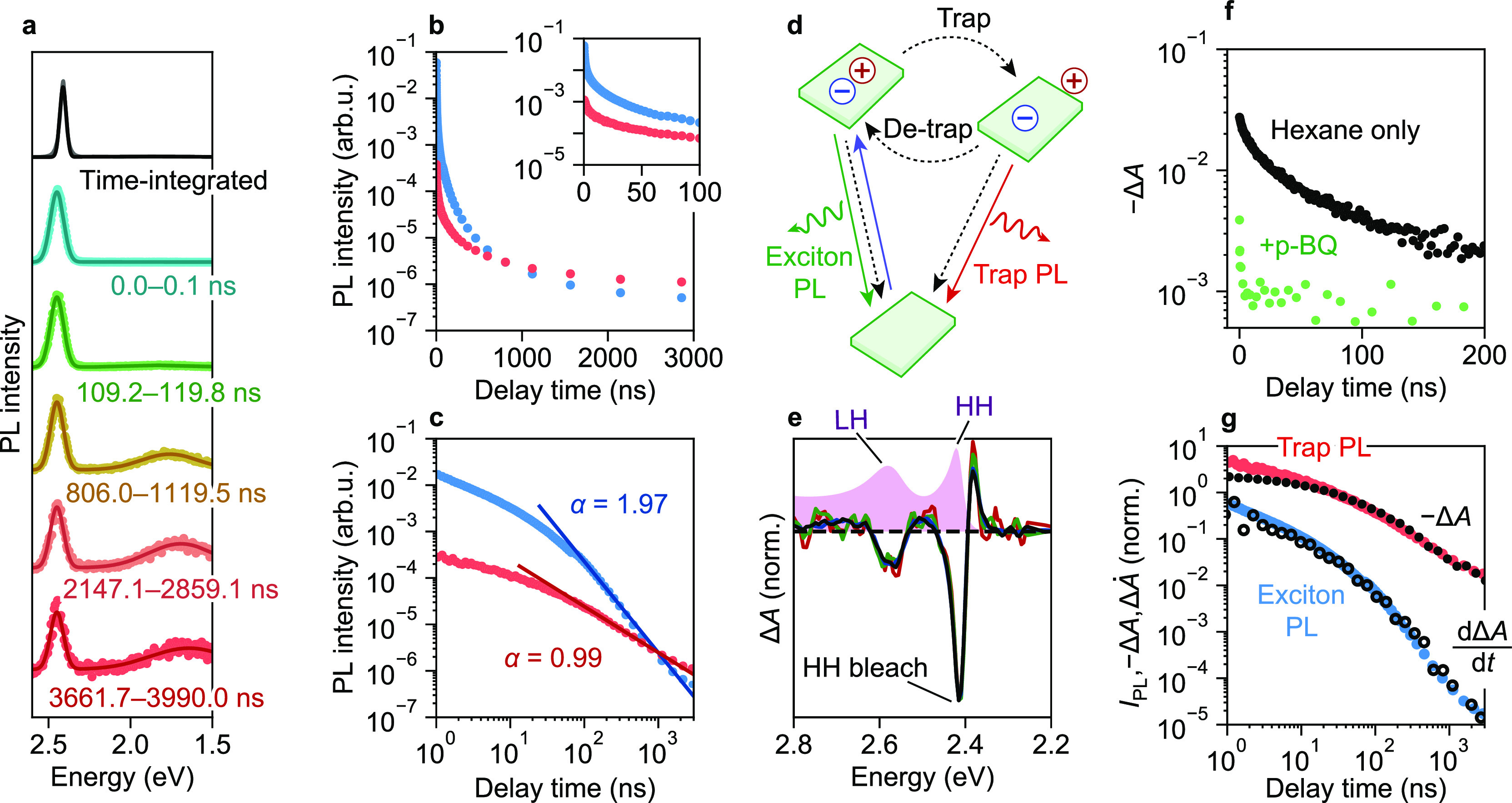
(a) PL spectra as a function of delay time fitted to a combination of two Gaussians. (Black) Steady-state PL spectrum, measured using a standard spectrometer, (cyan–red) time-resolved PL spectra, showing a relative increase in trap PL intensity, and red shift of trap PL with time, measured using a custom-built setup (Supporting Information). The time-resolved spectra are broadened due to the limited resolution of our custom setup. (b) Integrated intensities of the (blue) exciton and (red) trap PL peaks, as a function of delay time; the inset shows a zoom-in of the first 100 ns. (c) The same data as in (b), but displayed on double-logarithmic axes. Solid lines in (c) are fits to power-law decay I ∝ t–α, with I the PL intensity, t the delay time, and α the power-law slope, fitted on the interval [100, 3000] ns. (d) Three-state model explaining delayed and trap emission in CdSe nanoplatelets: after photoexcitation, one charge carrier can localize at a (surface) trap. Direct radiative recombination of the trapped charge carrier is possible, yielding trap PL, or the charge carrier may detrap. The black dashed lines indicate nonradiative transitions. (e) (Solid lines) Transient absorption spectra of an ensemble of CdSe nanoplatelets dispersed in hexane, normalized to the HH bleach feature, recorded at delay times of (black) 0.0, (blue) 11.3, (green) 119, and (red) 215 ns; (pink area) steady-state absorption spectrum of the same sample. The HH and LH absorption features are indicated. (f) HH bleach −ΔA as a function of delay time, for CdSe nanoplatelets dispersed in hexane with (black) no additives and (green) added p-BQ. (g) Time dependence of the (blue) exciton and (red) trap PL intensity, (black solid symbols) the HH bleach −ΔA, and (black open circles) the time derivative of the HH bleach, dΔA/dt, of CdSe NPLs dispersed in hexane.
TA spectra of an ensemble of CdSe NPLs (excitation wavelength 355 nm, pulse duration 650 ps), measured up to microseconds after excitation, show a bleach of the heavy-hole (HH) and light-hole (LH) features, as well as induced absorption features, red-shifted with respect to the steady-state spectrum (Figure 1e). These bleach features were previously attributed to state filling,44 while the induced-absorption features are likely due to favorable exciton–exciton or trion interactions. The shape of the TA spectrum is virtually independent of delay time (Figure 1e), indicating that a single spectroscopic species dominates the spectrum. The long lifetime suggests that this species corresponds to a state in which one charge carrier is trapped. The bleach of the HH feature must be due to the remaining delocalized charge carrier. Since both a delocalized electron and/or hole could in principle induce a bleach of the HH feature, these experiments do not reveal which charge carrier remains localized and which one is trapped. Therefore, we performed additional TA experiments, in which the NPLs are exposed to hole and electron scavengers, revealing which charge carrier remains delocalized and which one is trapped. We find that the addition of the hole quencher ethanol45 influences the bleach recovery only little (Figure S2), whereas electron extraction by p-benzoquinone (p-BQ)46 leads to a substantial decrease in the initial bleach amplitude and very rapid bleach recovery (Figure 1f). We conclude that, in the absence of p-BQ, photogenerated electrons that occupy the conduction band cause the HH bleach. The trapped charge carrier is thus the photogenerated hole.
In Figure 1g we show the TA bleach recovery together with the exciton and trap PL decay. Here, we use the magnitude of the HH bleach feature as an indicator for the total excited-state population, constituting a population X of NPLs with a free exciton and a population S of NPLs in which the hole is trapped. We find that, for t > 50 ns, the TA bleach recovery dynamics matches the trap PL decay, which indicates that at these time scales almost all holes are stored in a trap state (i.e., −A ∝ S). The time derivative of the TA bleach dynamics, on the other hand, matches with the delayed exciton PL decay, in line with the model in which the exciton PL scales with the derivative of the trap population dS/dt (Supporting Information, Section S2). Hence, these TA measurements confirm that delayed and trap PL are due to the same distribution of trap states.
It is unclear how the distribution of trap states and corresponding widely distributed rate constants affect individual NPLs. We performed single-NPL measurements on two batches of NPLs, similar in size, shape, and spectral properties (Supporting Information). NPL batch I was used for measurement series “A”, in which the NPLs were not treated; batch II was used for series “B”, in which the microscope sample was rinsed with butylamine after NPL deposition, thereby removing surface ligands and inducing a larger fraction of trap PL.1 In Figure 2 we present results from a measurement on a single NPL that showcases our diverse single-particle observations (see Extended Data for all single-particle results; the NPL of Figure 2 is “CdSe NPL 5”). The NPL exhibits both exciton and trap PL (Figure 2a). Both types of PL fluctuate in intensity (Figure 2b), indicating the transient presence of quenching pathways. We have selected four time periods (colored regions in Figure 2a,b) to highlight the fluctuations in the PL spectrum and lifetime. During the yellow and green periods, the NPL emitted only exciton PL, narrowly peaked around 2.41 eV throughout the experiment (Figure 2a,c). Although both time periods exhibit virtually identical PL intensities and spectra, they display markedly different PL decay. During the yellow period, the decay is dominated by a component with a lifetime of 39 ns, whereas the lifetime is 102 ns during the green period (Figure 2d). Both decay curves appear biexponential, with a short lifetime component on the order of a few nanoseconds (Figure 2e). These observations agree well with the reversible-trapping model depicted in Figure 1d, which predicts biexponential exciton decay for a single NPL (Supporting Information, Section S2). On the other hand, these observations contradict diffusion-based models,47,48 which predict power-law single-particle decay. In the framework of reversible trapping, the fast decay component is due to prompt exciton PL immediately following excitation, occurring before any hole-trapping event, thus competing with trapping. The slow decay component is due to detrapping and subsequent delayed emission. The observation of exponential decay of the slow component with a fluctuating decay rate indicates that (i) a single detrapping process with a specific rate is active at any moment in time but (ii) the detrapping rate fluctuates on a time scale of seconds. This must mean that the energetic position of the trap state with respect to the edge of the valence band fluctuates on this time scale, suggesting a connection between the chemical nature of the trap state and its depth.35 These fluctuations in the detrapping rate result in a single-NPL decay curve containing many different exponential components, yielding the apparent power-law decay observed in the ensemble.
Figure 2.
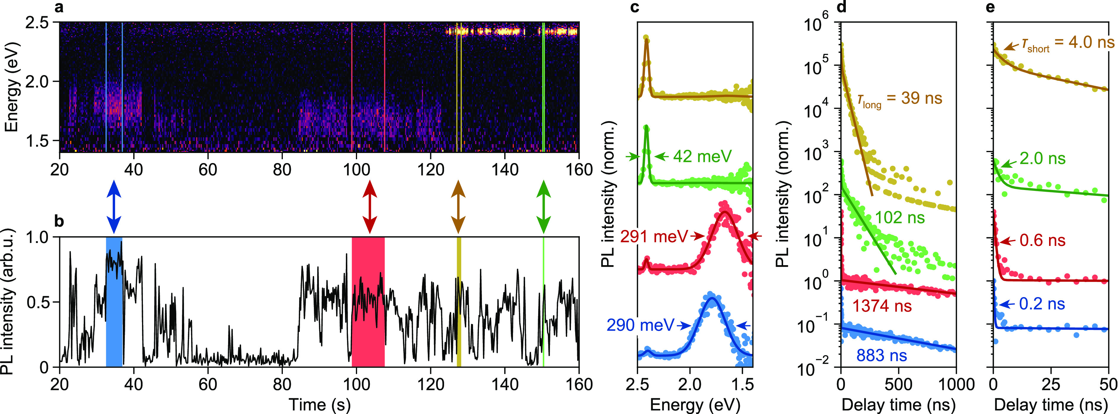
Results of measurements on a single CdSe NPL from the untreated “A” microscopy sample: (a) PL spectra and (b) intensity as a function of time; (c) PL spectra and (d) PL decay curves, constructed from the four colored regions indicated in panels (a) and (b). (e) The same data as depicted in panel (d), but displayed on shorter time scales. Lines are fits to (c) two Gaussian peaks and (d, e) biexponential decay. The fitted (c) full-width at half-maxima and (d) long-component and (e) short-component PL lifetimes τ are indicated. The PL intensities plotted in panel (b) are the sum of the exciton and trap peak integrals, which were determined by fitting each emission spectrum to two Gaussian peaks.
During the red and blue periods, indicated in Figure 2a,b, the NPL emits predominantly trap PL. The trap PL spectrum is much broader than the excitonic PL and exhibits spectral diffusion: compared to the spectrum of the blue period, the spectrum of the red period has shifted to lower energies by 121 meV (Figure 2c). Apart from such distinct spectral jumps, we also observe more continuous changes in the trap peak position for some NPLs (Extended Data). Whereas we observe no trap PL during the yellow and green periods, we do observe a small excitonic peak in the spectrum of both the red and the blue period (Figure 2c). During the blue and red periods, the decay is extremely slow, with lifetimes on the order of 1 μs (Figure 2d). In addition, the decay curves of both periods exhibit a fast sub-nanosecond component (Figure 2e). This behavior is also in agreement with reversible trapping from the band edge: the fast component is due to prompt exciton PL that competes with hole trapping, while the slow component is likely dominated by radiative trap decay.
The variety of the emission behaviors that we observe in our single NPL must be due to fluctuations in the competition between charge carrier trapping, detrapping, and recombination. To understand this, we consider three scenarios: (i) no or relatively inefficient trapping, resulting in predominantly prompt exciton PL and a small fraction of delayed exciton PL (Figure 3a); (ii) fast trapping–detrapping cycles, yielding both prompt and delayed exciton PL, as well as trap PL (Figure 3b); and (iii) irreversible trapping, yielding prompt exciton PL and trap PL (Figure 3c). We parametrize the scenarios in terms of the probability of trapping from the exciton state Pt (determined by the rates of trapping and radiative exciton recombination) and the probability of detrapping from the trapped state Pdt (determined by the rates of detrapping and radiative trap recombination). Figure 3d shows the calculated lifetime of the slow decay component τslow and the average number of trapping–detrapping cycles N that precede eventual radiative recombination, as a function of Pt and Pdt (Supporting Information, Section S2). Long lifetimes occur when the NPL spends a significant amount of time in the trapped state. This happens in both scenario ii (rapid trapping–detrapping cycles; Pt is large and Pdt is large; N is large) and scenario iii (irreversible trapping; small Pdt; N is small). In Figure 3e we show the fraction of trap PL compared to total PL IT/Itot, neglecting nonradiative recombination (Supporting Information, Section S2). As one might expect, trap PL constitutes the largest portion of the total PL when Pt is large, while this fraction decreases for increasing Pdt.
Figure 3.

(a–c) Three (de)trapping regimes that CdSe NPLs may experience: (a) no trapping, (b) fast trapping–detrapping cycling, and (c) irreversible trapping. (d) Calculated lifetime of the slow delay component τslow, normalized to the trap recombination lifetime τT, and (e) fractional trap PL IT/Itot, as a function of trapping probability Pt and detrapping probability Pdt. The dotted lines in (d) and (e) are contours of the calculated average number of trapping events N prior to recombination. (f) Configuration–coordinate diagram, illustrating exciton and trap emission. (g) Zoom-in of the diagram displayed in panel (f), indicating the energy barriers for trapping ΔEtrap# and detrapping ΔEdetrap. As the single-NPL trap-PL fwhm appears to be independent of the peak energy (Figure S3; Extended Data), the difference in the equilibrium Q among trap states is negligible; that is, the trap states are spaced vertically, not horizontally, in the coordinate diagram.
For all four highlighted periods in Figure 2, the slow decay component is dominant, indicating that trapping is highly probable. It is difficult to estimate whether trapping is reversible or irreversible during the red and blue periods, as both small and large detrapping probabilities are possible (Figure 3e). The green and yellow periods exhibit no trap PL, suggesting that Pdt approaches unity. Our observations are thus evidence that multiple trapping–detrapping cycles (N > 1, Figure 3d) preceded radiative recombination during the green and yellow periods.
The trap PL spectra are as broad as 290 meV fwhm on the single-NPL level. This indicates strong phonon coupling, which, along with the PL lifetimes as slow as ∼1 μs, is consistent with the radiative recombination of a localized charge carrier.43 Exciton PL, in contrast, shows significantly less phonon coupling, resulting in line widths of 42 meV. This difference between exciton and trap PL is illustrated in a configuration–coordinate diagram, which depicts the energies of exciton and trap states along with the geometrical distortions (Figure 3f). We attribute the widely distributed (de)trapping rates to a distribution of possible trap-state energies (Figure 3f,g). In this model, the trapping and the detrapping rate are determined by the corresponding activation energies and thus depend on the energy of the trapped state (Figure 3g). As we will discuss below, spectral diffusion of trap PL—and not of exciton PL—also agrees with trap PL involving a surface-localized charge carrier.
We confirmed that our microscopy experiments were done on single NPLs using cross-correlation measurements. NPLs emitting predominantly exciton PL exhibit a significant zero-delay peak in their cross-correlation curves. This peak decreases in magnitude, relative to the side peaks, when a time-gating analysis is performed (Figure 4a), indicating that it is caused by biexciton emission.49 This trend was observed before in CdSe NPLs and attributed to a high biexciton QY.50,51 In contrast, we consistently observe perfect antibunching from NPLs that emit predominantly trap PL (Figure 4b). This means that rapid Auger recombination quenches any two-photon emission from doubly excited NPLs. As Auger recombination of delocalized charge carriers in NPLs is relatively inefficient,50,51 the trapped hole likely acts as a strong Auger acceptor, as was previously suggested for trapped electrons in CdSe/CdS/ZnS core/shell/shell NCs.52 Antibunched trap PL is not proof of a single active trap in a NPL, as a double-excited state with two trapped holes and two delocalized electrons could also be quenched by Auger recombination. The conclusion that one radiative trap state available at any one time follows from the PL decay curves (Figure 4d): an exponential long component of the trap PL decay (rather than multiexponential slow decay) is a signature of a single active trap state at any moment. The nature of the trap state in different NPLs differs, as reflected by the different lifetimes of the long components.
Figure 4.
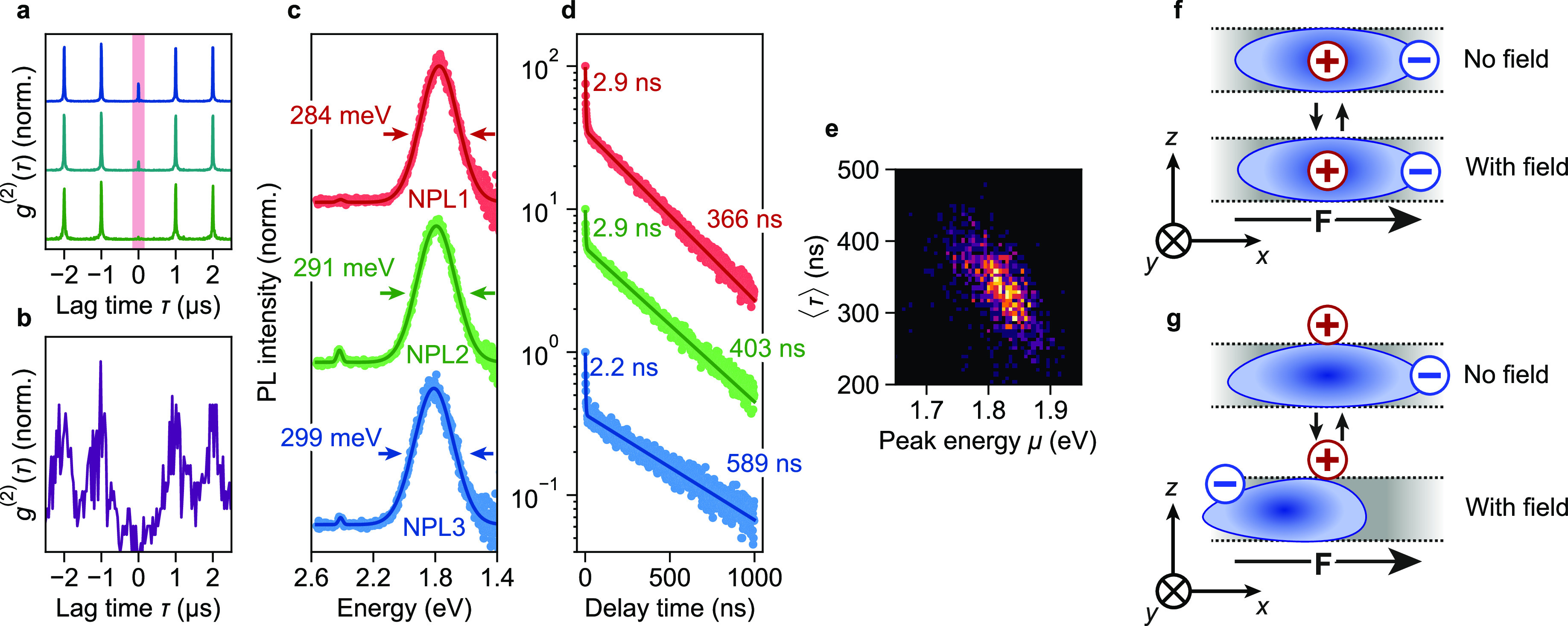
(a) Cross-correlation function g(2) of a CdSe NPL emitting predominantly exciton PL, for gate times of (blue, top) 0 (i.e., no time-gating), (cyan, middle) 1.00, and (green, bottom) 4.00 ns. (b) Cross-correlation function g(2) of a CdSe NPL emitting predominantly trap PL. (c) PL spectra and (d) PL decay curves of three different NPLs. Symbols are data points, solid lines are fits to (c) two Gaussian peaks and (d) biexponential decay. The fitted (c) fwhm and (d) lifetimes are indicated. The PL decay curves were collected without spectral selectivity, so they include dominant trap PL and any weak exciton PL. (e) Two-dimensional histogram showing the correlation of fitted peak energy μ and average photon arrival time ⟨τ⟩ of a trap-emitting NPL that exhibited spectral diffusion. (f, g) Cartoons illustrating the (lack of) electron–hole pair polarizability. The cartoons depict a cross-cut of a NPL, with the x,y axes corresponding to the lateral directions, and F the external electric field. Hypothetical hole localization (f) inside the NPL or (g) at the NPL surface results in qualitatively different polarizabilities. The NPL of panel (a) belonged to the untreated “A” microscopy sample; the NPLs of panels (b)–(e) to the butylamine-treated “B” sample.
Individual NPLs with nearly identical trap PL spectra (Figure 4c) exhibit biexponential PL decay with slightly different lifetimes (Figure 4d). This indicates that the lifetime is not determined exclusively by the activation energy for detrapping (ΔEdetrap# in Figure 3g). Additional (slow) recombination pathways or different pre-exponential factors in the Arrhenius equation may explain the different kinetics. The fast lifetime component of the trap-emitting NPLs (Figure 4d) may be due to fast exciton PL in competition with hole trapping. Alternatively, it may be due to flickering of trap PL:53 blinking of trap PL on time scales faster than the spectral integration time, with a fast decay component due to competition with fast nonradiative recombination.
Trap PL shows spectral diffusion with a consistently negative correlation between trap PL peak position and lifetime; that is, the PL energy increases as the lifetime decreases, and vice versa (Figure 4e). Such spectral diffusion has been observed in spherical QDs as well, where it was attributed to the quantum-confined Stark effect.8,9 In this effect transient electric fields—likely generated by charges on the nanocrystal surface—54 interact with the exciton,6 inducing a negative correlation between peak energy and lifetime. Dielectric confinement of the exciton to the quasi-2D NPL volume facilitates a strong electron–hole interaction, resulting in a very low polarizability and, consequently, a weak response to electric fields. This explains why the exciton PL does not show spectral diffusion and the ensemble exciton PL peak is as narrow as 46 meV fwhm.
In the case of trap PL, dielectric-confinement-enhanced Coulomb attraction between the delocalized electron and the trapped hole would depend on where the hole localizes. Hole localization inside the NPL would lead to Coulomb interactions similarly strong to those for the free exciton, preventing polarization (Figure 4f). However, for hole localization on the NPL surface, the electron–hole interaction would be weaker, resulting in a larger polarizability (Figure 4g). We can model this effect in a simplified fashion by approximating the electron–hole pair as a 2D hydrogen atom (Supporting Information, Section S3). This yields polarizabilities of 20, 40, and 3 × 10³ Å3 for an electron bound to a hole trapped inside the NPL, for a free exciton, and for an electron bound to a hole trapped on the NPL surface, respectively. In comparison, excitons in CdSe QDs can have much larger polarizabilities up to 105 Å3 depending on the QD size.6 For fields of 130 MV/m (corresponding roughly to two opposite charges spaced by 3 nm), a polarizability of 3 × 10³ Å3 would yield a red shift of ∼50 meV, similar in magnitude to the shifts observed experimentally (Figure 2a,c; Figure 4e). In comparison, the shift expected for an exciton in a NPL is negligible, only 0.5 meV. The occurrence of spectral diffusion thus shows that the trapped state consists of a surface-localized hole and a delocalized electron.
Conclusions
In conclusion, we have shown how individual trap states determine the luminescence properties of individual CdSe NPLs. The exciton PL decay of single NPLs is approximately biexponential over periods of seconds, indicating the involvement of a trap with fixed charge-carrier trapping and detrapping rates. Nonetheless, the lifetimes of the two components fluctuate in time, consistent with spontaneous fluctuations of these rates on time scales of seconds. This indicates that either the one active trap in a NPL changes its properties or a NPL contains multiple trap states that are active in turns, alternating on macroscopic time scales. A model incorporating reversible trapping from the band edge explains the single-NPL and ensemble dynamics of prompt, delayed, and trap PL well. NPLs sometimes switch from predominantly emitting exciton PL to predominantly emitting trap PL, or viceversa, indicating a spontaneous structural change that affects the availability of traps and/or the associated (de)trapping rates. In contrast with exciton PL, trap PL is antibunched, broad, slow, and susceptible to spectral diffusion. The latter three properties point to the involvement of a surface-localized charge carrier, which TA measurements have shown to be the photogenerated hole. Our observations show that, due to reversible trapping, the large radiative decay rate of CdSe NPLs is virtually irrelevant for many applications: the decay dynamics are dominated by trapping–detrapping kinetics. These results highlight the importance of trap-state passivation in the use of semiconductor NCs as spectrally narrow and fast-emitting fluorophores. Future studies, employing computational methods55 or sub-nanosecond structural characterization,56,57 may shed more light on the chemical identity of trap states in semiconductor NCs.
Experimental Section
Chemicals
1-Butanol (BuOH, anhydrous, 99.8%), cadmium acetate (Cd(OAc)2, 99.995%), cadmium nitrate tetrahydrate (Cd(NO3)2·4H2O, 98%), cadmium acetate dihydrate (Cd(OAc)2·2H2O, 98%), n-hexane (anhydrous, 95%), methanol (MeOH, anhydrous 99.8%), 1-octadecene (ODE, 90%), oleic acid (OA, 90%), butylamine (99.5%), p-benzoquinone (p-BQ, ≥98%), and sodium myristate (NaMyr, 99%) were purchased from Sigma-Aldrich. Methanol (MeOH, GPR Recatpur 99.5%), Se (200 mesh), and sodium acetate (Na(OAc)) were purchased from VWR, Strem Chemicals, and Merck, respectively. All chemicals were used as received, without additional purification, unless noted otherwise.
Synthesis of Cadmium Myristate
Cd(NO3)2·4H2O (1.23 g, 3.99 mmol) was dissolved in MeOH (40 mL). In a separate beaker, NaMyr (3.13 g, 12.5 mmol) was dissolved in MeOH (250 mL). After complete dissolution of both salts, the Cd-containing solution was added slowly to the NaMyr solution. The mixture was filtered using a Büchner funnel, and the white, solid product was thoroughly washed with MeOH and dried overnight.
Synthesis of CdSe Nanoplatelets
The 4.5-monolayer-thick CdSe nanoplatelets were prepared in a N2-filled glovebox following the procedure of Bertrand etal.,58 with minor modifications. ODE (15 mL), Cd(Myr)2 (0.170 g), and Se (0.012 g) were placed in a 50 mL round-bottom flask. The mixture was heated to 240 °C. The acetate mixture (see below) was added swiftly upon reaching 195 °C. The particles were grown at 240 °C for 5 min, after which the reaction was quenched by addition of hexane (14 mL) and removal of the heating mantle. Once the mixture had cooled to 95 °C, OA (1 mL) was added, and the mixture was allowed to cool to room temperature. The NPLs were precipitated by addition of BuOH/MeOH (2:1, v/v) and centrifugation at 3000 rpm and subsequently redispersed in n-hexane. The 4.5-monolayer-thick NPLs were separated from the byproducts (quantum dots and NPLs of different thickness) by size-selective precipitation using a BuOH/MeOH (2:1, v/v) mixture.
Acetate Mixtures Used in CdSe Nanoplatelet Synthesis
Three different batches of CdSe NPLs have been used in this work (see below). For batch I, solely anhydrous Cd(OAc)2 (0.0854 g) was used. For batches II and III, a mixture of Cd(OAc)2 (0.0403 g) and Cd(OAc)2·2H2O (0.0466 g) was used.
NPL Batches Used in Experiments
The CdSe NPLs used in the experiments were not colloidally stable over extended periods of time (months). Therefore, different batches of NPLs were used for the different experiments, as summarized in Table S2. Although different batches were used, the NPL properties (shape, size, and absorption spectrum) are comparable (Figure S1). Two series of single-NPL experiments were performed: “A”, with as-synthesized NPLs; “B”, with NPLs that were treated with butylamine, to decrease the ligand coverage. The former NPLs exhibit predominantly exciton PL (see Table S3), whereas the latter NPLs showed predominantly trap PL (see Table S3 and the Extended Data, provided in the Supporting Information).
Transmission Electron Microscopy
Samples were prepared for electron microscopy by drop-casting a NPL dispersion onto carbon-coated polymer film, attached to a copper TEM grid. Samples were imaged using a FEI Talos F200X electron microscope, operated at 200 kV.
Steady-State Ensemble-Scale Spectroscopy
For ensemble-scale steady-state spectroscopy, NPLs were diluted in n-hexane and placed in airtight 10 × 10 mm2 quartz cuvettes. Absorption spectra were recorded using an absorption spectrometer (PerkinElmer Lambda 950 UV/vis). Emission spectra were recorded on a home-built setup, in which the sample was excited by a 405 nm laser diode, and a lens pair projected the luminescence onto a fiber that guided the light to a spectrometer (Ocean Optics HR4000).
Sample Preparation for Single-Particle Measurements
The NPL dispersion was diluted 105–106× with anhydrous n-hexane. Under ambient atmosphere, the NPLs were spin-coated onto a #1.5 glass coverslip, which was subsequently attached to a glass microscope slide using double-sided tape. For the single-NPL “B” experiments, the coverslips were rinsed with butylamine after NPL deposition, to remove a fraction of the surface ligands and induce a larger portion of trap PL.38
Fluorescence Microscopy Experiments
Single-NPL measurements were performed on a home-built microscopy setup. This setup consisted of a Nikon Ti–U inverted microscope, on which the sample was placed. The excitation light source was a 405 nm ps-pulsed diode laser (Picoquant D-C-405), operated at a repetition rate of 1 MHz. The excitation light was guided into an oil-immersion objective (Nikon CFI Plan Apochromat Lambda 100×, NA 1.45) by a dichroic long-pass mirror. Before entering the microscope, the excitation beam was guided through an iris with a diameter of 2.0 mm. This underfilling of the objective back-aperture reduces the effective NA for excitation. We thus obtain a slightly larger diffraction-limited excitation spot, which makes the measurements less sensitive to drift. We estimate that the used excitation power resulted in, on average, 0.1 and 0.9 excitations per pulse, for the “A” and “B” experiments, respectively (see Supporting Information, Section S2). PL was collected by the same objective and filtered by suitable long-pass filters to remove reflected excitation light. The PL signal was then directed to one of two detection setups: (i) two avalanche photodiodes (APDs; Micro Photon Devices PDM) in Hanbury Brown–Twiss configuration or (ii) a setup in which a nonpolarizing beamsplitter directed half of the PL into a spectrograph (Andor Kymera 193i), equipped with an electron-multiplying charge-coupled device detector (EMCCD; Andor iXon Ultra 888), and the other half onto an APD. The wavelength-dependent detection efficiency of the spectrograph–EMCCD pair was corrected for using a broadband calibration light source (Ocean Optics, HL-3plus-CAL). The EMCCD detector, APDs, and laser driver (Picoquant PDL 800-D) were connected to a time-to-digital converter (qutools quTAG), which communicated the spectrum-recording, laser-pulse, and photon-detection events to a computer. Live time-correlated single-photon data visualization and storage was performed using home-written software.59
Fluorescence Microscopy Data Processing and Analysis
Custom Python scripts were used to process and analyze the single-NPL data. The raw data obtained from the time-to-digital converter contains a list of time tags for each signal received from our instruments: the APDs, the EMCCD camera, and the laser driver. The event lists from the laser driver and APD signals are compared to calculate the delay time for each photon detected. For each APD separately, a constant delay-time correction is then determined from the temporal position of the decay curve maximum. This correction time accounts for, among other factors, a time lag between the signals from laser driver and APD due to different cable lengths and light travel time. The negative delay times t that this produces are shifted by a laser pulse period T via t → t + T. Such photons, which were detected close to the rise in the decay curve (originating from the instrument response function), were ignored in the further data analysis. Our APDs exhibit so-called afterpulsing: after a valid photon detection event, there is a probability that the APD reports a false photon detection event. We removed such after-pulsing events in postprocessing by using only the first photon detection event per laser pulse and per detector for further analysis and discarding any other events. We confirmed that we measured emission from an individual NPL, instead of multiple NPLs, by measuring the cross-correlation g(2)(τ) between two detectors in Hanbury Brown–Twiss configuration. A relatively low correlation at lag time τ = 0, compared to the side-peaks at ± the laser pulse period (1000 ns), confirms that we detect emission from an individual (nearly) single-photon emitter. We additionally performed a time-gating analysis on the correlation data (see Figure 4a, as well as the Extended Data), to confirm that we were studying a single NPL when there was a zero-delay peak present. The event list of the EMCCD channel contains the times at which the camera started integrating individual spectra. With the data from this channel and known camera integration time, the start and end time of each spectral recording were calculated. These start and end times, in turn, were used to link each detected photon on the APD to a corresponding spectrum. The spectral integration time was 18 and 50 ms during the single-NPL “A” and “B” measurements, respectively. To improve the signal/noise ratio in the data analysis PL spectra were combined to obtain an effective integration time of 200 ms for both experiments.
Time-Resolved Emission Spectroscopy
Time-resolved emission spectroscopy (TRES) was performed using the same microscope as used in the single-particle measurements. However, TRES measurements were performed on an ensemble of CdSe NPLs, dispersed in anhydrous n-hexane. The sample was held in a custom-made airtight glass sample holder, which was filled inside a N2-filled glovebox. The sample holder was fixed to the sample stage and imaged using a custom objective (f = 30 mm, magnification = 6.67), based on an aspherized achromatic lens (Edmund Optics, #49-662). The sample was stirred throughout the measurements. A 150 μm pinhole was placed in an intermediate image plane (magnification = 6.67), to limit spectral broadening due to collection of out-of-focus PL. Half of the PL was guided to an APD, and the other half was guided to a galvomirror (Thorlabs GVS011/M). The galvomirror reflected the light onto a transmission grating (Edmund Optics #46-068, 70 lines/mm), and the first diffraction order was Fourier imaged onto the active area (diameter = 20 μm) of an APD by an f = 20 mm aspherized achromatic lens (Edmund Optics #49-569). The galvomirror was rotated over a set range of angles at a frequency of 2 Hz using a function generator (Agilent), thereby scanning the PL spectrum over the APD active area. For each detected photon we calculated the photon arrival time t* relative to the start of the corresponding galvomirror scan. These t* values were converted to wavelengths using the output of a white-light laser source (NKT SuperK EXTREME, equipped with an LLTF-Contrast wavelength selector) as calibration reference (Figure S4). The sample was excited using a 405 nm ps-pulsed laser (PicoQuant D-C-405), operated at a repetition rate of 250 kHz and a power of approximately 121 nW. Before entering the microscope, the excitation beam was guided through a 7.0 mm diameter iris, resulting in an effective excitation numerical aperture (NA) of 0.12.
Transient Absorption Spectroscopy
Transient absorption spectroscopy was performed using an EOS multichannel pump–probe transition absorption spectrometer (UltraFast Systems LLC). Inside a N2-filled glovebox, samples were placed in 1 mm path length quartz cuvettes. These cuvettes were sealed and placed in the measurement setup. The samples were stirred using ∼0.5 cm metal wires cut from paperclips. A collimated 355 nm pump beam was guided through a 1.8 mm diameter iris before it excited the sample and was obtained from subsequent second-harmonic and sum-frequency generation of a 1064 nm (pulse duration 650 ps fwhm) Nd:YAG laser (STANDA), operated at 1 kHz. The change in absorbance was obtained by measuring the transmission of the white-light spectrum (200–2400 nm, 200 mW, pulse duration <1 ns, repetition rate 2 kHz) obtained from a supercontinuum light source (LEUKOS), which was focused on the sample. Spectra were measured using a fiber-coupled multichannel spectrometer with a CMOS detector (spectral resolution of 1.5 nm). The white light was split into a probe beam and a reference beam; the latter was used to correct for fluctuations in the probe intensity.
Acknowledgments
This work was supported by The Netherlands Center for Multiscale Catalytic Energy Conversion (MCEC), an NWO Gravitation Programme funded by the Ministry of Education, Culture and Science of the government of The Netherlands. B.S. and D.V. wish to acknowledge the Dutch Research Council NWO (TOP-grant with project no. 715.016.002). D.V. wishes to acknowledge the European Research Council (ERC Advanced Grant “First Step” no. 692691). E.M.H. acknowledges support from the Dutch Research Council NWO (VI.Veni.192.034). S.J.W.V. and F.T.R. acknowledge financial support from the Dutch Research Council NWO (VENI-722.017.002 and OCENW.KLEIN.008).
Supporting Information Available
The Supporting Information is available free of charge at https://pubs.acs.org/doi/10.1021/acsnano.1c00481.
Estimation of the excitation regime, details and derivations related to modeling, ensemble-scale characterization of the samples studied; extended data, an overview of single-NPL results for all NPLs studied (PDF)
Author Contributions
The manuscript was written through contributions of all authors. All authors have given approval to the final version of the manuscript.
The authors declare no competing financial interest.
Supplementary Material
References
- Boles M. A.; Ling D.; Hyeon T.; Talapin D. V. The Surface Science of Nanocrystals. Nat. Mater. 2016, 15, 141–153. 10.1038/nmat4526. [DOI] [PubMed] [Google Scholar]
- Kovalenko M. V.; Manna L.; Cabot A.; Hens Z.; Talapin D. V.; Kagan C. R.; Klimov V. I.; Rogach A. L.; Reiss P.; Milliron D. J.; Guyot-Sionnest P.; Konstantatos G.; Parak W. J.; Hyeon T.; Korgel B. A.; Murray C. B.; Heiss W. Prospects of Nanoscience with Nanocrystals. ACS Nano 2015, 9, 1012–1057. 10.1021/nn506223h. [DOI] [PubMed] [Google Scholar]
- Talapin D. V.; Lee J.; Kovalenko M. V.; Shevchenko E. V. Prospects of Colloidal Nanocrystals for Electronic and Optoelectronic Applications. Chem. Rev. 2010, 110, 389–458. 10.1021/cr900137k. [DOI] [PubMed] [Google Scholar]
- Hanifi D. A.; Bronstein N. D.; Koscher B. A.; Nett Z.; Swabeck J. K.; Takano K.; Schwartzberg A. M.; Maserati L.; Vandewal K.; Van de Burgt Y.; Salleo A.; Alivisatos A. P. Redefining Near-Unity Luminescence in Quantum Dots with Photothermal Threshold Quantum Yield. Science 2019, 363, 1199–1202. 10.1126/science.aat3803. [DOI] [PubMed] [Google Scholar]
- Rabouw F. T.; Van der Bok J. C.; Spinicelli P.; Mahler B.; Nasilowski M.; Pedetti S.; Dubertret B.; Vanmaekelbergh D. Temporary Charge Carrier Separation Dominates the Photoluminescence Decay Dynamics of Colloidal CdSe Nanoplatelets. Nano Lett. 2016, 16, 2047–2053. 10.1021/acs.nanolett.6b00053. [DOI] [PubMed] [Google Scholar]
- Empedocles S. A.; Bawendi M. G. Quantum-Confined Stark Effect in Single CdSe Nanocrystallite Quantum Dots. Science 1997, 278, 2114–2117. 10.1126/science.278.5346.2114. [DOI] [PubMed] [Google Scholar]
- Müller J.; Lupton J. M.; Rogach A. L.; Feldmann J.; Talapin D. V.; Weller H. Monitoring Surface Charge Migration in the Spectral Dynamics of Single CdSe CdS Nanodot/Nanorod Heterostructures. Phys. Rev. B: Condens. Matter Mater. Phys. 2005, 72, 205339. 10.1103/PhysRevB.72.205339. [DOI] [Google Scholar]
- Ihara T.; Kanemitsu Y. Spectral Diffusion of Neutral and Charged Exciton Transitions in Single CdSe/ZnS Nanocrystals Due to Quantum-Confined Stark Effect. Phys. Rev. B: Condens. Matter Mater. Phys. 2014, 90, 195302. 10.1103/PhysRevB.90.195302. [DOI] [Google Scholar]
- Hinterding S. O. M.; Vonk S. J. W.; Van Harten E. J.; Rabouw F. T. Dynamics of Intermittent Delayed Emission in Single CdSe/CdS Quantum Dots. J. Phys. Chem. Lett. 2020, 11, 4755–4761. 10.1021/acs.jpclett.0c01250. [DOI] [PMC free article] [PubMed] [Google Scholar]
- Geiregat P.; Houtepen A. J.; Sagar L. K.; Infante I.; Zapata F.; Grigel V.; Allan G.; Delerue C.; Van Thourhout D.; Hens Z. Continuous-Wave Infrared Optical Gain and Amplified Spontaneous Emission at Ultralow Threshold by Colloidal HgTe Quantum Dots. Nat. Mater. 2018, 17, 35–41. 10.1038/nmat5000. [DOI] [PubMed] [Google Scholar]
- Coolen L.; Brokmann X.; Spinicelli P.; Hermier J. P. Emission Characterization of a Single CdSe-ZnS Nanocrystal with High Temporal and Spectral Resolution by Photon-Correlation Fourier Spectroscopy. Phys. Rev. Lett. 2008, 100, 027403. 10.1103/PhysRevLett.100.027403. [DOI] [PubMed] [Google Scholar]
- Sallen G.; Tribu A.; Aichele T.; André R.; Besombes L.; Bougerol C.; Richard M.; Tatarenko S.; Kheng K.; Poizat J. P. Subnanosecond Spectral Diffusion Measurement Using Photon Correlation. Nat. Photonics 2010, 4, 696–699. 10.1038/nphoton.2010.174. [DOI] [Google Scholar]
- Fernée M. J.; Littleton B.; Plakhotnik T.; Rubinsztein-Dunlop H.; Gómez D. E.; Mulvaney P. Charge Hopping Revealed by Jitter Correlations in the Photoluminescence Spectra of Single CdSe Nanocrystals. Phys. Rev. B: Condens. Matter Mater. Phys. 2010, 81, 155307. 10.1103/PhysRevB.81.155307. [DOI] [Google Scholar]
- Fernée M. J.; Plakhotnik T.; Louyer Y.; Littleton B. N.; Potzner C.; Tamarat P.; Mulvaney P.; Lounis B. Spontaneous Spectral Diffusion in CdSe Quantum Dots. J. Phys. Chem. Lett. 2012, 3, 1716–1720. 10.1021/jz300456h. [DOI] [PubMed] [Google Scholar]
- Sher P. H.; Smith J. M.; Dalgarno P. A.; Warburton R. J.; Chen X.; Dobson P. J.; Daniels S. M.; Pickett N. L.; O’Brien P. Power Law Carrier Dynamics in Semiconductor Nanocrystals at Nanosecond Timescales. Appl. Phys. Lett. 2008, 92, 101111. 10.1063/1.2894193. [DOI] [Google Scholar]
- Rabouw F. T.; Kamp M.; Van Dijk-Moes R. J. A.; Gamelin D. R.; Koenderink A. F.; Meijerink A.; Vanmaekelbergh D. Delayed Exciton Emission and Its Relation to Blinking in CdSe Quantum Dots. Nano Lett. 2015, 15, 7718–7725. 10.1021/acs.nanolett.5b03818. [DOI] [PubMed] [Google Scholar]
- Marchioro A.; Whitham P. J.; Nelson H. D.; De Siena M. C.; Knowles K. E.; Polinger V. Z.; Reid P. J.; Gamelin D. R. Strong Dependence of Quantum-Dot Delayed Luminescence on Excitation Pulse Width. J. Phys. Chem. Lett. 2017, 8, 3997–4003. 10.1021/acs.jpclett.7b01426. [DOI] [PubMed] [Google Scholar]
- Nirmal M.; Dabbousi B. O.; Bawendi M. G.; Macklin J. J.; Trautman J. K.; Harris T. D.; Brus L. E. Fluorescence Intermittency in Single Cadmium Selenide Nanocrystals. Science 1996, 383, 802–804. [Google Scholar]
- Kuno M.; Fromm D. P.; Hamann H. F.; Gallagher A.; Nesbitt D. J. Nonexponential “Blinking” Kinetics of Single CdSe Quantum Dots: A Universal Power Law Behavior. J. Chem. Phys. 2000, 112, 3117–3120. 10.1063/1.480896. [DOI] [Google Scholar]
- Rabouw F. T.; Antolinez F. V.; Brechbühler R.; Norris D. J. Microsecond Blinking Events in the Fluorescence of Colloidal Quantum Dots Revealed by Correlation Analysis on Preselected Photons. J. Phys. Chem. Lett. 2019, 10, 3732–3738. 10.1021/acs.jpclett.9b01348. [DOI] [PMC free article] [PubMed] [Google Scholar]
- Boehme S. C.; Azpiroz J. M.; Aulin Y. V.; Grozema F. C.; Vanmaekelbergh D.; Siebbeles L. D. A.; Infante I.; Houtepen A. J. Density of Trap States and Auger-Mediated Electron Trapping in CdTe Quantum-Dot Solids. Nano Lett. 2015, 15, 3056–3066. 10.1021/acs.nanolett.5b00050. [DOI] [PubMed] [Google Scholar]
- Busby E.; Anderson N. C.; Owen J. S.; Sfeir M. Y. Effect of Surface Stoichiometry on Blinking and Hole Trapping Dynamics in CdSe Nanocrystals. J. Phys. Chem. C 2015, 119, 27797–27803. 10.1021/acs.jpcc.5b08243. [DOI] [Google Scholar]
- Yao J.; Larson D. R.; Vishwasrao H. D.; Zipfel W. R.; Webb W. W. Blinking and Nonradiant Dark Fraction of Water-Soluble Quantum Dots in Aqueous Solution. Proc. Natl. Acad. Sci. U. S. A. 2005, 102, 14284–14289. 10.1073/pnas.0506523102. [DOI] [PMC free article] [PubMed] [Google Scholar]
- Ebenstein Y.; Mokari T.; Banin U. Fluorescence Quantum Yield of CdSe/ZnS Nanocrystals Investigated by Correlated Atomic-Force and Single-Particle Fluorescence Microscopy. Appl. Phys. Lett. 2002, 80, 4033–4035. 10.1063/1.1482785. [DOI] [Google Scholar]
- Brokmann X.; Coolen L.; Dahan M.; Hermier J. P. Measurement of the Radiative and Nonradiative Decay Rates of Single CdSe Nanocrystals through a Controlled Modification of Their Spontaneous Emission. Phys. Rev. Lett. 2004, 93, 107403. 10.1103/PhysRevLett.93.107403. [DOI] [PubMed] [Google Scholar]
- Pons T.; Medintz I. L.; Farrell D.; Wang X.; Grimes A. F.; English D. S.; Berti L.; Mattoussi H. Single-Molecule Colocalization Studies Shed Light on the Idea of Fully Emitting versus Dark Single Quantum Dots. Small 2011, 7, 2101–2108. 10.1002/smll.201100802. [DOI] [PubMed] [Google Scholar]
- Ithurria S.; Dubertret B. Quasi 2D Colloidal CdSe Platelets with Thicknesses Controlled at the Atomic Level. J. Am. Chem. Soc. 2008, 130, 16504–16505. 10.1021/ja807724e. [DOI] [PubMed] [Google Scholar]
- Tessier M. D.; Javaux C.; Maksimovic I.; Loriette V.; Dubertret B. Spectroscopy of Single CdSe Nanoplatelets. ACS Nano 2012, 6, 6751–6758. 10.1021/nn3014855. [DOI] [PubMed] [Google Scholar]
- Ithurria S.; Tessier M. D.; Mahler B.; Lobo R. P. S. M.; Dubertret B.; Efros A. L. Colloidal Nanoplatelets with Two-Dimensional Electronic Structure. Nat. Mater. 2011, 10, 936–941. 10.1038/nmat3145. [DOI] [PubMed] [Google Scholar]
- Morgan D. P.; Kelley D. F. Exciton Localization and Radiative Lifetimes in CdSe Nanoplatelets. J. Phys. Chem. C 2019, 123, 18665–18675. 10.1021/acs.jpcc.9b04639. [DOI] [Google Scholar]
- Drijvers E.; De Roo J.; Martins J. C.; Infante I.; Hens Z. Ligand Displacement Exposes Binding Site Heterogeneity on CdSe Nanocrystal Surfaces. Chem. Mater. 2018, 30, 1178–1186. 10.1021/acs.chemmater.7b05362. [DOI] [Google Scholar]
- Saniepay M.; Mi C.; Liu Z.; Abel E. P.; Beaulac R. Insights into the Structural Complexity of Colloidal Cdse Nanocrystal Surfaces: Correlating the Efficiency of Nonradiative Excited-State Processes to Specific Defects. J. Am. Chem. Soc. 2018, 140, 1725–1736. 10.1021/jacs.7b10649. [DOI] [PubMed] [Google Scholar]
- Anderson N. C.; Hendricks M. P.; Choi J. J.; Owen J. S. Ligand Exchange and the Stoichiometry of Metal Chalcogenide Nanocrystals: Spectroscopic Observation of Facile Metal-Carboxylate Displacement and Binding. J. Am. Chem. Soc. 2013, 135, 18536–18548. 10.1021/ja4086758. [DOI] [PMC free article] [PubMed] [Google Scholar]
- Kirkwood N.; Monchen J. O. V.; Crisp R. W.; Grimaldi G.; Bergstein H. A. C.; Du Fossé I.; Van der Stam W.; Infante I.; Houtepen A. J. Finding and Fixing Traps in II-VI and III-V Colloidal Quantum Dots: The Importance of Z-Type Ligand Passivation. J. Am. Chem. Soc. 2018, 140, 15712–15723. 10.1021/jacs.8b07783. [DOI] [PMC free article] [PubMed] [Google Scholar]
- Houtepen A. J.; Hens Z.; Owen J. S.; Infante I. On the Origin of Surface Traps in Colloidal II-VI Semiconductor Nanocrystals. Chem. Mater. 2017, 29, 752–761. 10.1021/acs.chemmater.6b04648. [DOI] [Google Scholar]
- Leemans J.; Singh S.; Li C.; Brinck S.; Ten Bals S.; Infante I.; Moreels I. Near-Edge Ligand Stripping and Robust Radiative Exciton Recombination in CdSe/CdS Core/Crown Nanoplatelets. J. Phys. Chem. Lett. 2020, 11, 3339–3344. 10.1021/acs.jpclett.0c00870. [DOI] [PMC free article] [PubMed] [Google Scholar]
- Giansante C.; Infante I. Surface Traps in Colloidal Quantum Dots: A Combined Experimental and Theoretical Perspective. J. Phys. Chem. Lett. 2017, 8, 5209–5215. 10.1021/acs.jpclett.7b02193. [DOI] [PMC free article] [PubMed] [Google Scholar]
- Singh S.; Tomar R.; Ten Brinck S.; De Roo J.; Geiregat P.; Martins J. C.; Infante I.; Hens Z. Colloidal CdSe Nanoplatelets, A Model for Surface Chemistry/Optoelectronic Property Relations in Semiconductor Nanocrystals. J. Am. Chem. Soc. 2018, 140, 13292–13300. 10.1021/jacs.8b07566. [DOI] [PubMed] [Google Scholar]
- Schwartz O.; Tenne R.; Levitt J. M.; Deutsch Z.; Itzhakov S.; Oron D. Colloidal Quantum Dots as Saturable Fluorophores. ACS Nano 2012, 6, 8778–8782. 10.1021/nn302551v. [DOI] [PubMed] [Google Scholar]
- Palato S.; Seiler H.; McGovern L.; MacK T. G.; Jethi L.; Kambhampati P. Electron Dynamics at the Surface of Semiconductor Nanocrystals. J. Phys. Chem. C 2017, 121, 26519–26527. 10.1021/acs.jpcc.7b09145. [DOI] [Google Scholar]
- Kalyuzhny G.; Murray R. W. Ligand Effects on Optical Properties of CdSe Nanocrystals. J. Phys. Chem. B 2005, 109, 7012–7021. 10.1021/jp045352x. [DOI] [PubMed] [Google Scholar]
- Mack T. G.; Jethi L.; Kambhampati P. Strategy for Exploiting Self-Trapped Excitons in Semiconductor Nanocrystals for White Light Generation. ACS Photonics 2019, 6, 1118–1124. 10.1021/acsphotonics.9b00212. [DOI] [Google Scholar]
- Mooney J.; Krause M. M.; Saari J. I.; Kambhampati P. Challenge to the Deep-Trap Model of the Surface in Semiconductor Nanocrystals. Phys. Rev. B - Condens. Matter Mater. Phys. 2013, 87, 081201(R) 10.1103/PhysRevB.87.081201. [DOI] [Google Scholar]
- Geiregat P.; Tomar R.; Chen K.; Singh S.; Hodgkiss J. M.; Hens Z. Thermodynamic Equilibrium between Excitons and Excitonic Molecules Dictates Optical Gain in Colloidal CdSe Quantum Wells. J. Phys. Chem. Lett. 2019, 10, 3637–3644. 10.1021/acs.jpclett.9b01607. [DOI] [PubMed] [Google Scholar]
- Carroll G. M.; Brozek C. K.; Hartstein K. H.; Tsui E. Y.; Gamelin D. R. Potentiometric Measurements of Semiconductor Nanocrystal Redox Potentials. J. Am. Chem. Soc. 2016, 138, 4310–4313. 10.1021/jacs.6b00936. [DOI] [PMC free article] [PubMed] [Google Scholar]
- Wu K.; Liang G.; Shang Q.; Ren Y.; Kong D.; Lian T. Ultrafast Interfacial Electron and Hole Transfer from CsPbBr3 Perovskite Quantum Dots. J. Am. Chem. Soc. 2015, 137, 12792–12795. 10.1021/jacs.5b08520. [DOI] [PubMed] [Google Scholar]
- Utterback J. K.; Grennell A. N.; Wilker M. B.; Pearce O. M.; Eaves J. D.; Dukovic G. Observation of Trapped-Hole Diffusion on the Surfaces of CdS Nanorods. Nat. Chem. 2016, 8, 1061–1066. 10.1038/nchem.2566. [DOI] [PubMed] [Google Scholar]
- Kurilovich A. A.; Mantsevich V. N.; Stevenson K. J.; Chechkin A. V.; Palyulin V. V. Complex Diffusion-Based Kinetics of Photoluminescence in Semiconductor Nanoplatelets. Phys. Chem. Chem. Phys. 2020, 22, 24686–24696. 10.1039/D0CP03744C. [DOI] [PubMed] [Google Scholar]
- Mangum B. D.; Ghosh Y.; Hollingsworth J. A.; Htoon H. Disentangling the Effects of Clustering and Multi-Exciton Emission in Second-Order Photon Correlation Experiments. Opt. Express 2013, 21, 7419. 10.1364/OE.21.007419. [DOI] [PMC free article] [PubMed] [Google Scholar]
- Ma X.; Diroll B. T.; Cho W.; Fedin I.; Schaller R. D.; Talapin D. V.; Gray S. K.; Wiederrecht G. P.; Gosztola D. J. Size-Dependent Biexciton Quantum Yields and Carrier Dynamics of Quasi-Two-Dimensional Core/Shell Nanoplatelets. ACS Nano 2017, 11, 9119–9127. 10.1021/acsnano.7b03943. [DOI] [PubMed] [Google Scholar]
- Hu Z.; Singh A.; Goupalov S. V.; Hollingsworth J. A.; Htoon H. Influence of Morphology on the Blinking Mechanisms and the Excitonic Fine Structure of Single Colloidal Nanoplatelets. Nanoscale 2018, 10, 22861–22870. 10.1039/C8NR06234J. [DOI] [PubMed] [Google Scholar]
- Van der Stam W.; Grimaldi G.; Geuchies J. J.; Gudjonsdottir S.; Van Uffelen P. T.; Van Overeem M.; Brynjarsson B.; Kirkwood N.; Houtepen A. J. Electrochemical Modulation of the Photophysics of Surface-Localized Trap States in Core/Shell/(Shell) Quantum Dot Films. Chem. Mater. 2019, 31, 8484–8493. 10.1021/acs.chemmater.9b02908. [DOI] [PMC free article] [PubMed] [Google Scholar]
- Galland C.; Ghosh Y.; Steinbrück A.; Sykora M.; Hollingsworth J. A.; Klimov V. I.; Htoon H. Two Types of Luminescence Blinking Revealed by Spectroelectrochemistry of Single Quantum Dots. Nature 2011, 479, 203–207. 10.1038/nature10569. [DOI] [PMC free article] [PubMed] [Google Scholar]
- Schival K. A.; Gipson R. R.; Prather K. V.; Tsui E. Y. Photoinduced Surface Charging in Iron-Carbonyl-Functionalized Colloidal Semiconductor Nanocrystals. Nano Lett. 2019, 19, 7770–7774. 10.1021/acs.nanolett.9b02726. [DOI] [PubMed] [Google Scholar]
- Bodnarchuk M. I.; Boehme S. C.; Ten Brinck S.; Bernasconi C.; Shynkarenko Y.; Krieg F.; Widmer R.; Aeschlimann B.; Günther D.; Kovalenko M. V.; Infante I. Rationalizing and Controlling the Surface Structure and Electronic Passivation of Cesium Lead Halide Nanocrystals. ACS Energy Lett. 2019, 4, 63–74. 10.1021/acsenergylett.8b01669. [DOI] [PMC free article] [PubMed] [Google Scholar]
- Kirschner M. S.; Hannah D. C.; Diroll B. T.; Zhang X.; Wagner M. J.; Hayes D.; Chang A. Y.; Rowland C. E.; Lethiec C. M.; Schatz G. C.; Chen L. X.; Schaller R. D. Transient Melting and Recrystallization of Semiconductor Nanocrystals under Multiple Electron-Hole Pair Excitation. Nano Lett. 2017, 17, 5315–5320. 10.1021/acs.nanolett.7b01705. [DOI] [PubMed] [Google Scholar]
- Oguz Er A.; Chen J.; Rentzepis P. M. Ultrafast Time Resolved X-Ray Diffraction, Extended X-Ray Absorption Fine Structure and X-Ray Absorption near Edge Structure. J. Appl. Phys. 2012, 112, 031101. 10.1063/1.4738372. [DOI] [Google Scholar]
- Bertrand G. H. V.; Polovitsyn A.; Christodoulou S.; Khan A. H.; Moreels I. Shape Control of Zincblende CdSe Nanoplatelets. Chem. Commun. 2016, 52, 11975–11978. 10.1039/C6CC05705E. [DOI] [PubMed] [Google Scholar]
- Hinterding S. O. M.; Rabouw F. T.. PHoton Arrival-Time STudio (PHAST). Zenodo 2020, 10.5281/zenodo.4354144. [DOI] [Google Scholar]
Associated Data
This section collects any data citations, data availability statements, or supplementary materials included in this article.