

Abstract
In this article, we investigate the application of polythiophene (PT), polythiophene with embedded gold nanoparticles (PT-Au), and polythiophene with embedded palladium nanoparticles (PT-Pd) via the spin coating technique on the rear contact of single-crystalline silicon solar cells. Several layers of coating (up to four layers) were applied, followed by a simple heat treatment at 70 °C for 30 min. The morphology, particles distribution in the polymer, and crystal structure of the colloid PT, PT-Au, and PT-Pd were characterized by transmission electron microscopy (TEM). Optical characteristics of the polymer and nanoparticles embedded in the polymers exhibited high absorption in the near-UV region, and a plasmonic peak at around 580 nm is observed. The calculated energy gap ranged from 2.65 eV (PT-Pd 5%) to 2.9 eV (PT) and 3.05 eV (PT-Au 5%). Scanning electron microscopy (SEM) images of the successive layers show an increase in the density and thickness of the PT particles with increasing number of coating layers, up to 12 μm for four layers of PT. Devices were characterized under dark conditions exhibiting variations in the ideality factor and series and shunt resistances with different coating layers. The silicon solar cells were characterized by measuring quantum efficiency, photoconversion efficiency (PCE), fill factor, and series and shunt resistances before and after coating. The coating was found to reduce the series resistance and to increase the efficiency of the cell by up to 7.25% for the PT-Au5% layers.
Introduction
The sunlight at earth’s surface consists of 44% actinic ray, 3% ultraviolet, and remaining is actinic ray. Since the atmosphere blocks 77% of the sun’s UV radiation, only infrared radiation hits earth. Photovoltaic cells absorb high-frequency radiations like ultraviolet and visual lights and convert them into electricity, whereas infrared (IR) may be a low-frequency radiation that is mostly converted to heat or thermal radiation.1 In normal silicon photoelectric cells, IR radiations just experience the electric cell that converts into heat and hence affect the efficiency. The use of nanomaterials and nanocomposites for photovoltaic cell applications has several benefits like reducing manufacturing cost as a result of employing the same temperature process as printing rather than the high-temperature vacuum deposition process, typically used to produce conventional solar cells made with crystalline semiconductor materials. It may also be coated over flexible rolls rather than rigid crystalline panels, making it suitable for roll-to-roll (R2R) production. Nanomaterials have a larger area-to-volume ratio than the opposite conventional forms, which improves chemical reactivity and increases the strength of the materials. Hence, it is cost-effective, durable, and highly efficient. Silicon is the most dominant commercial material utilized in the solar cell industry.2 Although Si accounts for about 90% of the worldwide production of solar cells, it still suffers from many issues that result in an overall efficiency reduction.3,4 However, these issues are often categorized into two main types: optical and electrical losses. Consequently, many researchers tend to boost the performance of Si solar cells so as to achieve the utmost possible efficiency. Transforming the unabsorbed sun radiation photons energy to photons with energies which will be utilized by the cell could significantly enhance the efficiency of the photoelectric cells.5,6 Optical conversion processes are considered to be the simplest ways to optically enhance the efficiency of Si solar cells by exploiting the unabsorbed infrared (IR) or ultraviolet (UV) solar spectra through optical conversions or photoluminescence mechanisms.7 Meanwhile, electrical losses are another source of problems thanks to the metal coverage shadowing losses, ohmic losses, temperature, and metal–insulator–semiconductor (MIS) barriers.8 These electrical issues mainly affect the cell conductivity and electrical I–V curve including electrical circuit voltage (Voc) and short-circuit current (Isc), therefore reducing the general power conversion efficiency (PCE) of the photovoltaic cell. Coating solar cells or panels with nanostructures have recently been extensively investigated to boost the efficiency of the cells.9 Intermediate dielectric layer (IDL) such as TiO2, for improving adhesion and obtaining larger crystalline silicon to enhance the direct Si–glass interface, was applied for thin-film silicon solar cells.10
A conducting polymer was used to make polymer solar cells (PSC).11 Polythiophene (PT) is a widely used donor material for solution-processed polymer solar cells. Much progress in PT-based PSCs is often attributed to the planning of novel PTs exhibiting intense and broad visible absorption with high charge carrier mobility to extend short-circuit current (Isc), together with low-lying highest occupied molecular orbital (HOMO) levels to achieve large open-circuit voltage (Voc) values.12
The incorporation of metal nanoparticles (NPs) as plasmonic into thin active layers is considered a successful strategy for the representation of presenting high efficiency of both organic solar cells and perovskite solar cells. This phenomenon rose from the significantly enhanced light absorption and electrical characteristics in fundamental.13 They demonstrated that plasmonic NPs can be incorporated easily into either the photoactive or the buffer layers or at interfaces for the enhancement of the optical absorption due to localized surface plasmon resonance (LSPR) and the light scattering effect and the enhancement of the electrical properties in the exciton dissociation, charge transport, and collection of the mentioned solar cells, without great change in the device architecture. Du et al.14 discussed the size effect of gold nanoparticles for the plasmon-induced charge transfer mechanism in 30 nm TiO2 systems assembled with gold nanoparticles of varying diameter. They utilized the femtosecond time-resolved IR-probe technique, and a fast electron injection (<240 fs) from the gold nanoparticle to TiO2 was observed. They also explored the charge transfer mechanisms and the effects of gold particle size on charge recombination kinetics as well as observed slower charge recombination dynamics in systems with larger gold particle diameters. Possible mechanisms including the behavior of hot holes were discussed, which will consider the study of the plasmon-induced electron transfer mechanism as a significant tool to demonstrate the effect of plasmonic NPs in the encasement of solar cell nanodevices.
High-performance inverted polymer solar cells are demonstrated by introducing a nanostructured backscattering rear electrode, with metal nanoparticles (NP) embedded into the hole extraction layer.15 Plasmonic metallic nanoparticles (NPs) have recently been identified as a breakthrough for enhancing the efficiency of organic photovoltaic devices. Different strategies of incorporating plasmonic NPs for light trapping into either the active layer or the buffer layer or at various interfaces within the organic photovoltaic cell architecture were attributed to the proposed different enhancement mechanisms.16 Different geometries have been tried, such as NPs dispersed into the active layer, NPs dispersed into the hole transport layer (PEDOT:PSS), NPs dispersed between interfacing layers, NPs combinations, and two-dimensional (2D) arrays of NPs,17 and several mechanisms have been suggested, such as charge transport, scattering, exciton quenching, LSPR + scattering, monomolecular recombination, strong local near-field, resistance reduction, near-field plasmonic, and far-field scattering.17
Traditional methods for polymer photovoltaic cell fabrication utilized solution processing techniques like spin coating, doctor blade, and inkjet printing. Polymer solar cells were prepared (polythiophene-sensitized),18 in dye-sensitized solar cells as a photosensitizer,19 by vacuum thermal evaporation (VTE) of (P3HT).20 Polymer solar cells have shown potential to utilize solar power in a very cost-effective way.
Efficient polymer solar cells supported a bulk heterojunction of (P3HT) and methanofullerene,21 deposited electrochemically,22 using it as a charge transport material in highly efficient and stable perovskite solar cells (PSCs),23 and polythiophene-fullerene-based solar cells.24,25 Fullerene-free polymer solar cells were also fabricated with polythiophene derivatives.26,27 Lanthanide-doped (LiYF4) upconversion nanoparticles into TiO2 film were reported developing a polythiophene–TiO2 heterojunction in addition to upconversion nanoparticles.28
Gold/polymer multilayer films exhibiting enhanced conductivity were also investigated. The films exhibited spherical gold nanoparticles (NPs) (around 3 nm diameter) homogeneously dispersed into a polymeric matrix. For increased response time and thiophene/gold precursor ratio, agglomerated gold structures in an exceedingly thin layer of polythiophene were obtained employing a simple and one-step synthesis of polythiophene/gold nanoparticles (PT/Au) nanocomposite thin films, through a liquid–liquid (L/L) interfacial polymerization route,29 functional nanocomposite-supported electrospun nanofibers coated with gold nanoparticles,30 synthesizing nanoscale polythiophene-gold nanoparticle (AuNP) hybrid systems assembled by the Langmuir–Blodgett (LB) method,31 and solution processing using gold nanoparticles and soluble polypyrrole or poly(3,4-ethylenedioxythiophene).32
Experimental Section
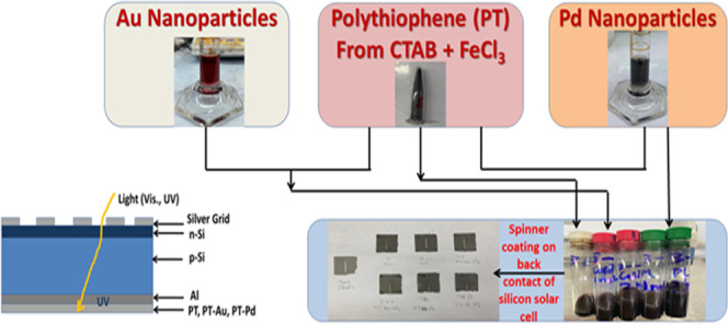
Figure 1 shows a flow diagram illustrating the experimental setup for producing PT, PT-Au, and PT-Pd, spin coating on back contact of silicon solar cell up to measuring the solar cell efficiency. Polythiophene (PT) was prepared as explained in ref (33). Thiophene (2.4 mmol) was mixed with 50 mL of chloroform in a reaction vessel. Then, 3.4 mmol of cetyltrimethyl ammonium bromide (CTAB) surfactant dissolved in 30 mL of chloroform was added to the monomer solution and stirred for 15 min. The molar ratio [monomer]/[surfactant] was 7:1. Finally, 5.5 mmol of anhydrous FeCl3 was dissolved in 170 mL of chloroform and added dropwise. Polymerization was carried out for 24 h at room temperature. The precipitate of polythiophene was collected by filtration and washed with chloroform. The PT was further washed with methanol to remove the residual oxidant. The PT powder was dried in a vacuum dryer at 50 °C for 24 h. Chlorauric acid (HAuCl4·3H2O, 50 mL, 0.01 wt %) solution was heated to boiling while stirring in a 100 mL beaker. Then, a few hundred microliters (μL) of 1 wt % trisodium citrate dihydrate (Na3C6H5O7·H2O) solution was quickly added to the auric solution. The color of the solution changed within several minutes from yellow to black and then to scarlet purple color, indicating the reduction process and the formation of Au nanoparticles. PdCl2 (30 mg) and poly(vinylpyrrolidone) (PVP, 250 mg) were added to equal 20 mL of distilled deionized (DDI) water with vigorous stirring for 30 min. The obtained assorted light orange solution was transferred to a lined stainless steel Teflon-type autoclave, and the system was adjusted at 150 °C for 18 h. After that, the Teflon vessel was cooled to room temperature and the tiny powder was isolated by repeated centrifugation at 10 000 rpm with repeated washing with water and ethanol thrice. Finally, the powder was dispersed in absolute ethanol before applying in PT. Gold and palladium were ultrasonically dispersed in the PT polymer using a Biologics, Inc. model 3000MP ultrasonic homogenizer for 30 min, with two concentrations of gold and palladium, 5 and 10% by weight each. Single-crystalline silicon solar cells of 150 × 150 mm2 were cut into smaller regular pieces of the total area between 8 to 9 cm2, as shown in Figure 1. Four successive PT layers were spin-coated on the rear surface of the solar cell using an APT GmbH Automation spin coater at a rotation speed of 1000 rpm at a rate of 50 rpm/s for 60 s for every layer. Heat treatment of all prepared films was done in Carbolite dryer at 70 °C for 30 min. All solar cells efficiencies were measured under AM1.5 conditions using a PET Photo Emission Tech, Inc. SS200ABA solar simulator, before and after coating, to compare the performances of the cell itself, and the measured cell temperature ranged from 25 to 27 °C, but it was the same for each cell. Ten successive measurements were carried out, and the average one was recorded. High-resolution transmission electron microscopy (TEM) (JEOL JEM-2100F) was used to investigate the morphology of the nanoparticles distribution in the polymer and to investigate the crystal structure of PT, PT-Au, and PT-Pd colloids. UV-visible absorption measurements were done for the colloids to record their absorbance in the visible, near-UV, and UV regions using a Spectro UV–vis Double Beam Labomed, Inc. spectrophotometer in the range from 0 to 1200 nm. Energy band gap calculations are done on these measurements to determine the allowed energy gap transition of these colloids. Scanning electron microscopy (SEM) measurements were carried out using a JEOL JSM-6360LA SEM with a scanning voltage of 15 kV for the successive layers of PT spin-coated on the back contact of the silicon solar cells. External quantum efficiency (EQE) and responsivity were measured for all of the prepared solar cells: as received Si, coated with PT, Pt-Au, and coated with PT-Pd using a monochromator utilizing a PVE300 system in a Bentham TMc300, with a 300 mm focal length monochromator, as described in ref (34). Dark I–V measurements were done under the application of a computer-controlled potentiostat (Metrohm Autolab, model: 87070) with a scan rate of 10 mV/s for a range between −1 V and +1 V.
Figure 1.

(a) Flow diagram illustrating the experimental setup for producing PT, PT-Au, and PT-Pd films via spin coating on back contact of silicon solar cell up to measuring solar cell efficiency. (b) Cross-sectional SEM image of the spin-coated Si solar cell with four PT layers. (c) Silicon solar cell structure with a possible mechanism of light passage in the entire cell.
Results and Discussion
Transmission electron microscopy (TEM) images of polythiophene (PT), gold embedded in polythiophene (PT-Au), and palladium embedded in polythiophene (PT-Pd) are shown in Figure 2. Low-resolution PT shows multilayers of the polymer decorated with dark points, which may be referred to residual iron nanoparticles raised from the PT preparation procedure, as shown in the inset of the PT figure. Selected area electron diffraction (SAED) pattern shown in the inset of the PT figure revealed the amorphous nature of the polythiophene polymer. For gold embedded in polythiophene (PT-Au), the Au nanoparticles with average diameters of 11–14 nm are well dispersed in the PT polymers. High-resolution transmission electron microscopy (HRTEM) of Au showed the fringes of the gold atoms with a d-spacing of 0.24 nm of the (111) plane. The SAED pattern shown in the inset of PT-Au confirms the existence of the (111), (200), (220), and (222) planes of the polycrystalline nature for the Au nanoparticles.35 For palladium embedded in polythiophene (PT-Pd), the Pd nanoparticles with average diameters of 3–5 nm are well dispersed in the PT polymer matrix. HRTEM of Pd shows the fringes of the palladium atoms with a d-spacing of 0.2 nm of the (111) plane. The SAED pattern shown in the inset of PT-Pd confirms the existence of the (111), (200), and (220) planes of the polycrystalline nature of the Pd nanoparticles.36,37
Figure 2.

Low-resolution TEM, HRTEM, and SAED images for PT, PT-Au, and PT-Pd used for spin coating on the rear contact of silicon solar cells.
Scanning electron microscopy (SEM) images of the spin-coated polythiophene on the Al back contact at low and high magnifications with one, two, three, and four layers are shown in Figure 3. With one layer of PT deposition, low-density particles of PT appeared and the aluminum microparticles of the back contact are clearly detected with particles’ average diameter between 1 and 5 μm. Increasing the number of spin-coated PT layers results in an increase in the density of the PT particles with an increase in the coated layers up to four layers of PT. The cross section of the four layers of PT/Al/Si gives an average thickness of about 12 μm, as shown in Figure 1c. The PT particles are compact in morphology and showed a layered structure, as evidenced from the TEM measurements shown in Figure 2. The PT layers exhibit good adhesion to the aluminum substrate.
Figure 3.

SEM of spin-coated polythiophene on Al back contact at low magnification (left) and high magnification (right) with one, two, three, and four layers.
Figure 4a shows the absorbance measurements of a colloidal solution of PT, PT-Au 5%, and PT-Pd 5%. The PT and PT-Au 5% samples show similar behavior of a plasmonic peak at a wavelength of about 580 nm, while the PT-Pd 5% sample has a lower intensity. For the three samples, there is a sharp increase in the absorbance starting from 400 to 300 nm. This near-UV high absorbance seemed to be of high interest to collect the dissipated UV light from the pn silicon junction for the improvement of their efficiency.38
Figure 4.
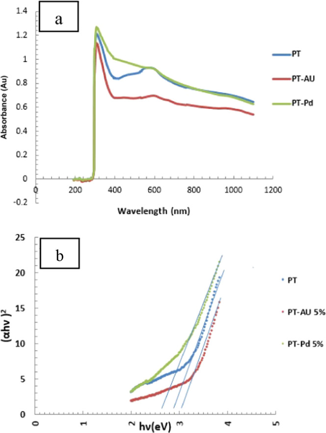
(a) Optical absorption spectra and (b) energy band gap calculations of PT, PT-Au 5%, and PT-Pd 5%.
The energy band gap (Eg) of PT, PT-Au 5%, and PT-Pd 5% is calculated from their absorption spectra, as shown in Figure 4b, using eq 1(39)
| 1 |
where (α) is the absorption coefficient of the materials, (hυ) is the light frequency, (Eg) is the energy band gap defined in eV, αo is a constant called band tailing parameter incident photon energy, and (n) is a parameter depending on the nature of the semiconductor. PT is known as a direct transition conducting polymer with semiconducting behavior, so n = (1/2).40
The band gap energies (Eg) are calculated and determined from the plot of (αhυ)2 vs (hυ). The interception of the regressed line with hν gives the value of the band gap energy (Eg). The calculated energy gap values ranged from 2.65 eV (PT-Pd 5%) to 2.9 eV (PT) and 3.05 eV (PT-Au 5%). These moderately high energy gap values coincide with the behavior of the absorbance given in Figure 4a as well as small nanoparticles of PT, Au, or Pd shown in Figure 2.
Figure 5 and Table 1 give the measured and calculated solar cell efficiency values including power values as well as series and shunt resistances for the spin-coated silicon PV devices with four layers of PT, PT-Au, and PT-Pd. For good and real comparison, all of the PV cells were measured before and after coating under the same measurement conditions (e.g., ambient temperature and solar cell radiation intensity of AM1.5) and a silicon reference cell was always used for adjusting the instrument intensity. The best improvement in efficiency was detected for the coating of PT-Au 5% with a 7.25% increase in the PCE, slightly higher than PT-only, which was 7.17%. For these cells, the most enhanced factor was the reduction of the series resistance of −19.7% for PT-Au 5% and −10.83% for the PT-only, as well as the resulting improvement in the fill factor. This reduction in series resistance significantly enhanced the values of the fill factor by 5.8% for PT-Au 5 and 5.99% for the PT. No significant enhancement for the shunt resistance is detected for all of the fabricated PT, PT-Au, and PT-Pd spin-coated layers on back contact. The decrease in series resistance and consequently improving the fill factor and efficiency for the PT and PT-Au 5% gives the benefit of applying the PT conducting polymer with or without an Au doping that absorbs UV light and improving the device series resistance. In contrast, PT-Pd 5% spin-coated layers increased the series resistance values by 9.2% and consequently reduced the photoconversion efficiency by 3.06%, which could be explained by the absorbance spectra (less plasmonic effect) and the lower energy gap value (2.65 eV), while the higher energy gap of 3.05 eV obtained for PT-Au 5% gave the higher improvement in the overall efficiency. This may be due to the well-dispersed Au nanoparticles onto the PT, as evidenced from Figure 2, and influenced the plasmonic effect, as shown in Figure 4a.
Figure 5.

I–V Curves for solar cells before and after spin coating of the back contact with (a) PT, (b) PT-Au, and (c) PT-Pd.
Table 1. Measured Silicon Solar Cells Efficiency Values, Open-Circuit Voltage, Short-Circuit Current Density, Fill Factor, Series and Shunt Resistances before and after Spin Coating of the Back Contact with Four Layers of PT, PT-Au, and PT-Pd.
| sample | polymer/nanocomposite | V∝ (mV) | JSC (mA/cm2) | FF (%) | efficiency (%) | Rs (Ω) | Rsh (Ω) | |
|---|---|---|---|---|---|---|---|---|
| 1 | PT-CTAB | before | 606.00 | 40.30 | 66.73 | 16.30 | 3.07 | 666.60 |
| after | 614.60 | 40.32 | 70.50 | 17.47 | 2.77 | 666.60 | ||
| increase % | 1.40 | 0.0004 | 5.99 | 7.17 | –10.83 | 0.00 | ||
| 2 | PT-CTAB Au 5% | before | 624.32 | 39.42 | 67.14 | 16.53 | 3.28 | 666.60 |
| after | 630.60 | 39.58 | 71.04 | 17.73 | 2.74 | 666.60 | ||
| increase % | 1.00 | 0.40 | 5.80 | 7.25 | –19.70 | 0.00 | ||
| 3 | PT-CTAB Au 10% | before | 628.90 | 36.60 | 70.90 | 16.30 | 2.96 | 666.60 |
| after | 632.80 | 36.09 | 72.15 | 16.48 | 2.89 | 671.40 | ||
| increase % | 0.62 | –1.41 | 1.76 | 1.10 | –2.42 | 0.68 | ||
Figure 6 shows the open-circuit voltage, Voc, and short-circuit current density, Jsc, of solar cells before and after spin coating of the back contact with PT-Au. An increase in Voc is noticed after coating for both PT-Au5% and PT-Au5% cells. Also a slight reduction in Jsc is noticed for the PT-Au10% cell. Figure 7 shows the fill factor (FF) of solar cells for the same samples. The FF increased by 5.65% for the PT-coated cell, 5.81% for the PT-Au5% coated cell, and 1.76% for the PT-Au10% coated cell.
Figure 6.

Open-circuit voltage, Voc, and short-circuit current density, Jsc, of solar cells before and after spin coating of the back contact with PT-Au.
Figure 7.

Fill factor (FF) of solar cells before and after spin coating of the back contact with PT-Au.
Figure 8a,b shows the measured external quantum efficiencies of solar cells before and after spin coating of the back contact with PT-Au and PT-Pd, respectively. PT-Au 5% displayed superior response to PT-Au 10% in the blue response (300–900 nm range) due to reduced front surface recombination, while PT-Au 10% was superior to PT-Au 5% sample in the red response (900–1100 nm range) due to reduced rear surface recombination, better absorption at long wavelengths, and higher diffusion length, with the latter two inferior to the noncoated sample. The PT-Pd 10% sample showed a deteriorated performance compared to PT-Pd 5%. Figure 9a,b shows the measured responsivity measurements for solar cells before and after spin coating of the back contact with PT-Au and PT-Pd, respectively.
Figure 8.

Quantum efficiency measurements for solar cells before and after spin coating of the back contact with (a) PT-Au and (b) PT-Pd.
Figure 9.

Responsivity measurements for solar cells before and after spin coating of the back contact with (a) PT-Au and (b) PT-Pd.
Figure 10a,b shows the measured dark I–V characteristics for solar cells before and after spin coating of the back contact with PT-Au and PT-Pd, respectively. It shows that PT-Au is superior to PT-Pd and that PT-Pd5% is worse than PT-Pd10%. Again, it is evident that the PT-Au samples outperform the PT-Pd ones.
Figure 10.

Dark I–V measurements for solar cells before and after spin coating of the back contact with (a) PT-Au and (b) PT-Pd.
In Figures 11 and 12, the dark ln I–V measurements in the range between 0.0 V and + 1 V are shown for solar cells before and after spin coating of the back contact with PT-Au and PT-Pd. The solar cell parameters were extracted from these measurements and are shown in Table 2, and a plot of the series and shunt resistances of the cells is shown in Figure 13 before and after spin coating of the back contact with PT-Au and PT-Pd. Increased Au% led to an increase of both series and shunt resistances. The same trend is observed for the PT-Pd samples, but PT-Pd5% showed an abnormally high series resistance, and therefore a much lower spectral response.
Figure 11.

Dark I–V measurements in the range between 0 and + 1 V for solar cells (a) without coating and (b) after spin coating of PT film on the back contact.
Figure 12.

Dark I–V measurements in the range between 0 and + 1 V for solar cells after spin coating of the back contact with (a) PT-Au and (b) PT-Pd.
Table 2. Parameters of the Sample Dark I–V Curve using One-Diode Model Parameter Extraction.
|
I0 (A) |
n |
||||||
|---|---|---|---|---|---|---|---|
| sample | Vth (V) | region 1 | region 2 | region 3 | region 1 | region | region 3 |
| Si without coating | 0.355 | 3 03 × 10–3 | 8.29 × 10⁻⁶ | 681 × 10–7 | 50.4 | 2 83 | 0.765 |
| PT | 0.35 | 2.48 × 10⁻³ | 3.72 × 10⁻⁵ | 5.03 × 10⁻⁶ | 11.3 | 3.44 | 1.11 |
| PT-Au 5% | 0.315 | 3.7 × 10⁻³ | 3.36 × 10⁻⁵ | 3.73 × 10⁻⁶ | 10.2 | 3.24 | 1.02 |
| PT-Au 10% | 0.34 | 3.52 × 10⁻³ | 2.04 × 10⁻⁵ | 1.52 × 10⁻⁶ | 0.131 | 3.25 | 0.957 |
| PT-Pd 5% | 0.3 | 3.03 × 10⁻⁴ | 6.79 × 10⁻⁶ | 14.92 | 0.92 | ||
| PT-Pd 10% | 0.3 | 4.09 × 10⁻³ | 6.77 × 10⁻⁵ | 4.12 × 10⁻⁶ | 0.37 | 4.7 | 0.98 |
Figure 13.

Variation of the series and shunt resistances of Si solar cells before and after the spin coating of the PT-Au and PT-Pd back contacts.
Conclusions
This work reports an investigation of using polymer coating on the back contact of single-crystalline silicon solar cells to increase the photoconversion efficiency of the solar cell. Polythiophene (PT), polythiophene embedded with gold nanoparticles (PT-Au), and polythiophene embedded with palladium nanoparticles (PT-Pd) were spin-coated on the rear contact of the PV cell. Preliminary results revealed a reduction of the series resistance and an increase in the nominal efficiency by up to 7.25%. Further optimization of the coating is expected to yield more improvement.
Acknowledgments
The authors acknowledge City of Scientific Research and Technological Applications (SRTA-City) for offering Research labs for the experimental and characterization tools used for this research. They gratefully thank and appreciate Prof. Mohamed M. Rashad and Dr. Ahmed Mortada for the measurements of the quantum efficiency of the prepared solar cells through their state-of-the-art facility at Central Metallurgical Research, Development Institute (CMRDI), Egypt.
The authors declare no competing financial interest.
References
- Kumar B.; Sivasankar G.; Sangeeth Kumar B.; Sundarapandy T.; Kottaisamy M. Development of Nano-composite Coating for Silicon Solar Cell Efficiency Improvement. Mater. Today: Proc. 2018, 5, 1759–1765. 10.1016/j.matpr.2017.11.273. [DOI] [Google Scholar]
- Ivaturi A.; Macdougall S. K.; Martín-Rodríguez R.; Quintanilla M.; Marques-Hueso J.; Krämer K. W.; Richards B. S.; et al. Optimizing infrared to near infrared upconversion quantum yield of -NaYF4:Er3 in fluoropolymer matrix for photovoltaic devices. J. Appl. Phys. 2013, 114, 013505 10.1063/1.4812578. [DOI] [Google Scholar]
- Rüdiger M.; Fischer S.; Frank J.; Ivaturi A.; Richards B. S.; Krämer K. W.; Goldschmidt J. C.; et al. Bifacial n-type silicon solar cells for upconversion applications. Sol. Energy Mater. Sol. Cells 2014, 128, 57–68. 10.1016/j.solmat.2014.05.014. [DOI] [Google Scholar]
- Fischer S.; Favilla E.; Tonelli M.; Goldschmidt J. C. Record efficient upconverter solar cell devices with optimized bifacial silicon solar cells and monocrystalline BaY2F8:30%Er3+ upconverter. Sol. Energy Mater. Sol. Cells 2015, 136, 127–134. 10.1016/j.solmat.2014.12.023. [DOI] [Google Scholar]
- Ji W.; Allen T.; Yang X.; Zeng G.; De Wolf S.; Javey A. Polymeric Electron-Selective Contact for Crystalline Silicon Solar Cells with an Efficiency Exceeding 19%. ACS Energy Lett. 2020, 5, 897–902. 10.1021/acsenergylett.0c00110. [DOI] [Google Scholar]
- Gibart P.; Auzel F.; Guillaume J.; Zahraman K. Below Band-Gap IR Response of Substrate-Free GaAs Solar Cells Using Two-Photon Up-Conversion. Jpn. J. Appl. Phys. 1996, 35, 4401–4402. 10.1143/JJAP.35.4401. [DOI] [Google Scholar]
- Strümpel C.; Mccann M.; Beaucarne G.; Arkhipov V.; Slaoui A.; Švřcek V.; Tobias I.; et al. Modifying the solar spectrum to enhance silicon solar cell efficiency—An overview of available materials. Sol. Energy Mater. Sol. Cells. 2007, 91, 238–249. 10.1016/j.solmat.2006.09.003. [DOI] [Google Scholar]
- van Dyk E.; Meyer E. Analysis of the effect of parasitic resistances on the performance of photovoltaic modules. Renewable Energy 2004, 29, 333–344. 10.1016/S0960-1481(03)00250-7. [DOI] [Google Scholar]
- Shehata N.; Clavel M.; Meehan K.; Samir E.; Gaballah S.; Salah M. Enhanced erbium-doped ceria nanostructure coating to improve solar cell performance. Materials. 2015, 8, 7663–7672. 10.3390/ma8115399. [DOI] [PMC free article] [PubMed] [Google Scholar]
- Çinar K.; Karaman M.; Bek A. Improvement of Laser-Crystallized Silicon Film Quality via Intermediate Dielectric Layers on a Glass Substrate. ACS Omega 2018, 3, 5846–5852. 10.1021/acsomega.8b00530. [DOI] [PMC free article] [PubMed] [Google Scholar]
- Mehmood U.; Al-Ahmed A.; Hussein I. Review on recent advances in polythiophene based photovoltaic devices. Renewable Sustainable Energy Rev. 2016, 57, 550–561. 10.1016/j.rser.2015.12.177. [DOI] [Google Scholar]
- Wang H.; Chen C.; Jeng R. Polythiophenes Comprising Conjugated Pendants for Polymer Solar Cells: A Review. Materials 2014, 7, 2411–2439. 10.3390/ma7042411. [DOI] [PMC free article] [PubMed] [Google Scholar]
- Li Y.; Kou Z.; Feng J.; Sun H. Plasmon-enhanced organic and perovskite solar cells with metal nanoparticles. Nanophotonics 2020, 9, 3111–3133. 10.1515/nanoph-2020-0099. [DOI] [Google Scholar]
- Du L.; Shi X.; Zhang G.; Furube A. Plasmon induced charge transfer mechanism in gold-TiO2 nanoparticle systems: The size effect of gold nanoparticle. J. Appl. Phys. 2020, 128, 213104 10.1063/5.0027108. [DOI] [Google Scholar]
- Cheng P.; Zhou L.; Li J.; Li Y.; Lee S.; Tang J. Light trapping enhancement of inverted polymer solar cells with a nanostructured scattering rear electrode. Org. Electron. 2013, 14, 2158–2163. 10.1016/j.orgel.2013.05.020. [DOI] [Google Scholar]
- Stratakis E.; Kymakis E. Nanoparticle-based plasmonic organic photovoltaic devices. Mater. Today 2013, 16, 133–146. 10.1016/j.mattod.2013.04.006. [DOI] [Google Scholar]
- Yu G.; Gao J.; Hummelen J. C.; Wudl F.; Heeger A. J. Polymer Photovoltaic Cells: Enhanced Efficiencies via a Network of Internal Donor-Acceptor Heterojunctions. Science 1995, 270, 1789. 10.1126/science.270.5243.1789. [DOI] [Google Scholar]
- Haeldermans I.; Truijen b I.; Vandewal K.; Moons W.; Van Bael M. K.; D’Haen J.; Manca J. V.; Mullens J. Water based preparation method for ‘green’ solid-state polythiophene solar cells. Thin Solid Films 2008, 516, 7245–7250. 10.1016/j.tsf.2007.12.023. [DOI] [Google Scholar]
- Siddiqui M. N.; Mansha M.; Mehmood U.; Nisar U.; Al-Betar A. F.; Al-Saadi A. A. Synthesis and characterization of functionalized polythiophene for polymer-sensitized solar cell. Dyes Pigm. 2017, 141, 406–412. 10.1016/j.dyepig.2017.02.041. [DOI] [Google Scholar]
- Lanzi M.; Di-Nicolaa; Errania F.; Paganina L.; Mucci A. Solventless deposition of oligo- and polythiophenes for bulk heterojunction solar cells. Synth. Met. 2014, 195, 61–68. 10.1016/j.synthmet.2014.05.016. [DOI] [Google Scholar]
- Li G.; Shrotriya V.; Huang J.; Yao Y.; Emery K.; Yang Y. High-efficiency solution processable polymer photovoltaic cells by self-organization of polymer blends. Nat. Mater. 2005, 4, 864–868. 10.1142/9789814317665_0012. [DOI] [Google Scholar]
- Nasybulin E.; Feinstein J.; Cox M.; Kymissis I.; Levon K. Electrochemically prepared polymer solar cell by three-layer deposition of poly(3,4-ethylenedioxythiophene)/poly(2,2'-bithiophene)/fullerene (PEDOT/PBT/C60). Polymer 2011, 52 (16), 3627–3632. 10.1016/j.polymer.2011.06.020. [DOI] [Google Scholar]
- Jeong I.; Woong Job J.; Baec S.; Sonc H.; Kod M. A fluorinated polythiophene hole-transport material for efficient and stable perovskite solar cells. Dyes Pigm. 2019, 164, 1–6. 10.1016/j.dyepig.2019.01.002. [DOI] [Google Scholar]
- Putnam D. G.Investigation of Degradation in Polythiophene-Fullerene Based Solar Cells. Graduate Theses and Dissertations. 2010, 11872, https://lib.dr.iastate.edu/etd/11872. [Google Scholar]
- Kim Y.; Choulis S. A.; Nelson J.; Bradley D.; Cook S.; Durrant J. R. Composition and annealing effects in polythiophene/fullerene solar cells. J. Mater. Sci. 2005, 40, 1371–1376. 10.1007/s10853-005-0568-0. [DOI] [Google Scholar]
- Christopher G.Recombination Dynamics in Polythiophene: Fullerene Solar Cells. Ph.D. Dissertation, Imperial College London, 2008. [Google Scholar]
- Qin Y.; Uddin M.; Chen Y.; Jang B.; Zhao K.; Zhong Z.; Yu H.; Shin T.; Woo H.; Hou J. Highly Efficient Fullerene-Free Polymer Solar Cells Fabricated with Polythiophene Derivative. Adv. Mater. 2016, 28, 9416–9422. 10.1002/adma.201601803. [DOI] [PubMed] [Google Scholar]
- Holliday S.; Ashraf R. S.; Wadsworth A.; Baran D.; Yousaf S. A.; Nielsen C. wB.; Tan C.; Dimitrov S. D.; Shang Z.; Gasparini N.; Alamoudi M.; et al. High-efficiency and air-stable P3HT-based polymer solar cells with a new non-fullerene acceptor. Nat. Commun. 2016, 7, 11585 10.1038/ncomms11585. [DOI] [PMC free article] [PubMed] [Google Scholar]
- Guo X.; Cui C.; Zhang M.; Huo L.; Huang Y.; Hou J.; Li Y. High efficiency polymer solar cells based on poly(3-hexylthiophene)/indene-C70 bisadduct with solvent additive. Energy Environ. Sci. 2012, 5, 7943–7949. 10.1039/c2ee21481d. [DOI] [Google Scholar]
- Ma X.; Ni X. Fabrication of polythiophene–TiO2 heterojunction solar cells coupled with upconversion nanoparticles. J. Mater. Sci. 2015, 26, 1129–1135. 10.1007/s10854-014-2516-8. [DOI] [Google Scholar]
- Inagaki C.; Oliveira M.; Gorgatti Zarbin A. Direct and one-step synthesis of polythiophene/gold nanoparticles thin films through liquid/liquid interfacial polymerization. J. Colloid Interface Sci. 2018, 516, 498–510. 10.1016/j.jcis.2018.01.076. [DOI] [PubMed] [Google Scholar]
- Sanfelice R. C.; Mercante L. A.; Pavinatto A.; Tomazio N. B.; Mendonca C. R.; Ribeiro S. J. L.; Mattoso L. H. C.; Correa D. S. Hybrid composite material based on polythiophene derivative nanofibers modified with gold nanoparticles for optoelectronics applications. J. Mater. Sci. 2017, 52, 1919–1929. 10.1007/s10853-016-0481-8. [DOI] [Google Scholar]
- Fathy M.; Wageh A.; El-Dissouky A.; Kashyout A.; Preparation of Polythiophene derivatives for hybrid solar cell devices., to be submitted.
- Karmalawi A. M.; Rayan D. M.; Rashad M. M. Establishment and evaluation of photovoltaic quantum efficiency system at central metallurgical research and development institute. Optik 2020, 217, 164931 10.1016/j.ijleo.2020.164931. [DOI] [Google Scholar]
- Jayaraman S.; Yu L.; Srinivasan M. P.. Polythiophene-gold Nanoparticle Hybrid Systems: Langmuir-Blodgett Assembly of Nanostructured Films, Nanoscale; The Royal Society of Chemistry, 2013. [DOI] [PubMed] [Google Scholar]
- Zotti G.; Vercelli B.; Berlin A. Gold Nanoparticle Linking to Polypyrrole and Polythiophene: Monolayers and Multilayers. Chem. Mater. 2008, 20, 6509–6516. 10.1021/cm801836j. [DOI] [Google Scholar]
- Wang C.; Hsao B.; Lai S.; Chen W.; Chen H.; Chen Y.; Chien C.; Cai X.; Kempson Ivan M.; Hwu Y.; Margaritondo G. One-pot synthesis of AuPt alloyed nanoparticles by intense x-ray irradiation. Nanotechnology 2011, 22, 065605 10.1088/0957-4484/22/6/065605. [DOI] [PubMed] [Google Scholar]
- Rajasekharreddy P.; Usha Rani P. Biosynthesis and Characterization of Pd and Pt Nanoparticles Using Piper betle L. Plant in a Photoreduction Method. J. Clust. Sci. 2014, 25, 1377–1388. 10.1007/s10876-014-0715-3. [DOI] [Google Scholar]
- Samir E.; Salah M.; Hajjiah A.; Shehata N.; Fathy M.; Hamed A. Electrospun PVA Polymer Embedded with Ceria Nanoparticles as Silicon Solar Cells Rear Surface Coaters for Efficiency Improvement. Polymers 2018, 10, 609 10.3390/polym10060609. [DOI] [PMC free article] [PubMed] [Google Scholar]
- Kamat S. V.; Tamboli S. H.; Puri V.; Puri R. K.; Yadav J. B.; Joo O. Post deposition heating effects on the properties of polythiophene thin films. Arch. Phys. Res. 2010, 1, 119–125. [Google Scholar]