

Abstract
Neural interfaces bridge the nervous system and the outside world by recording and stimulating neurons. Combining electrical and optical modalities in a single, hybrid neural interface system could lead to complementary and powerful new ways to explore the brain. It has gained robust and exciting momentum recently in neuroscience and neural engineering research. Here, we review developments in the past several years aiming to achieve such hybrid electrical and optical microsystem platforms. Specifically, we cover three major categories of technological advances: transparent neuroelectrodes, optical neural fibers with electrodes, and neural probes/grids integrating electrodes and microscale light-emitting diodes. We discuss examples of these probes tailored to combine electrophysiological recording with optical imaging or optical neural stimulation of the brain and possible directions of future innovation.
Keywords: neural interfaces, hybrid, transparent electrodes, optical fibers, LED
1. Introduction
Understanding the brain has always been challenging yet rewarding. Over the past centuries, our knowledge on our own brain has exploded from both studying the brain mechanisms and exploring therapeutic interventions for neurological disorders like epilepsy and Parkinson’s disease [1]. Concomitantly, various neural interface technologies have been developed, including optical and electrical methods, to probe and interrogate the brain [2–5]. Historically, Ramón y Cajal pioneered modern neuroscience by elucidating and recognizing the fundamental neuron-based microscopic structure of the brain in the late 19th century through improved Golgi staining and microscopy [6]. Observed by du Bois-Reymond though first in animal nerves [7], action potential was found to be the information carrier for cell-to-cell communication, which was later established by Nobel laureates Adrian Edgar and Charles Sherrington in the early 20th century [8, 9]. After that, the establishment of the ion-permeation-based mechanism by Hodgkin and Huxley in the 1950s has laid the foundation for the most of our knowledge of neuronal signaling [10, 11]. Measuring and interrogating neuronal signals therefore are crucial to the reverse engineering of the brain to understand normal or pathological dynamics of underlying neural circuits.
The brain, however, is extremely complex, containing networks of billions of neurons with different types, shapes, and complicated connections surrounding them. Conventional neuroelectrodes have proven their ability to probe the electrical activity from the brain with high temporal resolution but intrinsically lacks the spatial precision, while existing optical methods have established as the workhorse to reveal the finest spatial intricacies in brain tissue though they are still catching up in recording fast neuronal activities [12]. Combining these two modalities, in a single, hybrid platform could lead to complementary and powerful new ways to explore the brain and has gained much exciting momentum recently in neuroscience and neural engineering research [13]. As the device technology developed, biological aspects have also taken into consideration to minimize the damage of the brain and to maximize the device performance in terms of engineering perspective. During device implantation, it is crucial to understand the reaction of tissues in terms of cellular and molecular level to mitigate tissue damage, which would otherwise degrade the performance of devices in terms of signal sensitivity and longevity [14]. To reduce the footprint of the device implantation, developments in both materials and device designs have also been made to use softer materials to have better mechanical compliance with the brain and smaller devices to decrease the insertion footprint [15].
In this paper, we review developments in the past several years aiming to achieve such hybrid electrical and optical microsystem platforms. Specifically, we cover three major categories of technological advances, namely (i) transparent neuroelectrodes, (ii) optical neural fibers with electrodes, and (iii) neural probes/grids integrating electrodes and micro-light-emitting diodes (μ-LEDs). In the first category, transparent electrodes enable high spatiotemporal resolution of brain activity mapping since they are capable of recording/stimulating electrical neural activity, and allow optical imaging and interrogation of the neurons simultaneously. The combination of high temporal resolution from the electrophysiology recording and superior spatial resolution from optical imaging will bridge the fast neuronal networks to the underlying molecular and cellular structures in detail. For example, this method revealed spontaneous firing activity of single neurons in the brain network dynamics with corresponding spatial patterns in the cortical area [16]. The second and third categories are both related to optogenetics, a powerful new optical method that can deliver cell-type-specific stimulation of neurons [17], and modulates and controls the neural activity by light stimulating genetically modified neurons with light-sensitive opsins, such as channelrhodopsin-2 (ChR2) and halorhodopsin (NpHR). Significant improvements have been made recently for optogenetic tools in neurobiology including optical fibers and implantable probes [18–20]. The use of optical fiber has drawn considerable attention for effective light delivery in optogenetics due to its well-established optical waveguide property and miniaturized footprint [21]. Fiber-optic based hybrid platforms could offer various properties such as being compact, light-weight, immune to large dynamic range, electromagnetic interference, and their chemical and biological inertness in nature [22, 23]. On the other hand, μ-LEDs have emerged as the other popular means for localized light sources in optogenetics. Systems integrating electrodes with light stimulation capability has also been demonstrated, which incorporated μ-LED on a single or multiple shanks. Together, these hybrid electrical and optical neural interfaces, and their future developments will pave promising pathways for next-generation brain research.
2. Transparent neuroelectrodes
There has been tremendous progress in developing transparent electrodes in recent years, due to their capabilities of simultaneous electrical and optical recordings [24]. The state-of-the-art of microelectrode arrays (MEAs) have achieved high-density microelectrodes for recording and/or modulating of brain signals with electrical stimulation with high sensitivity and selectivity. However, electrode recording alone intrinsically lacks high-level of spatial resolution compared to optical imaging, which is critical as it allows to differentiate cell types, shapes, and complicated neural network connections among the brain cells. In the past, there have been the usage of optical imaging techniques to examine tissue surrounding electrode sites [25]. However, an exact correlation of neural signals with imaging data has been difficult. The development of completely transparent neuroelectrode devices is critical for next-level neural research, allowing both cortical imaging and optogenetic interventions concurrently with electrical recording. Over the past decade, a large number of studies aiming to integrate electrodes with optical imaging methods resulted in many different types of transparent electrodes to meet this need, which can be loosely categorized by the transparent electrode materials in use.
2.1. Indium tin oxide neuroelectrodes
Having high conductivity and transparency over the entire visible spectrum, transparent conductive oxides like indium tin oxide (ITO) have been utilized in numerous industrial applications. ITO has long been used in transparent and flexible applications, including displays, LEDs, solar cells and more recently in neural microelectrodes (Fig. 1a–d), due to its outstanding optical properties, such as extremely high transmittance and low auto-fluorescence. Figure 1a presents a 49-ch MEA using sputtered ITO as electrodes, gold (Au) as its interconnect and Parylene C as substrate [26]. It demonstrated 90% transparency and impedance of 30 kΩ with an electrode size of 250 μm in diameter. Parylene C is a widely used polymer for transparent and flexible neural devices, due to its biostability, biocompatibility, durability, lubricity, transparency, corrosion resistance, flexibility and surface consolidation, thus evading flaking or dusting [27]. Although ITO provides excellent electrical conductivity and transparency at the same time, it intrinsically has a brittle property [28]. To mitigate the brittleness, a hybrid structure of ITO and Au has been developed by confining ITO only to the electrodes while the long interconnect traces and bonding pads are fabricated with ductile Au (Fig. 1b) [29]. This opto-array showed 94% transparency and impedance of 1 ~ 5 kΩ with an electrode size of 200 μm in diameter, and utilized integrated LEDs for optical stimulation and simultaneous electrical recording. More about LED-integrated electrodes will be discussed in Section 4 of this review. Another ITO electrode array had 93% transparency and impedance of 345 kΩ with an electrode size of 100 μm in diameter and was able to facilitate two-photon imaging of Ca2+ signals and simultaneous electrical recording of cortical electroencephalogram (EEG) (Fig. 1c) [30]. They were able to perform the imaging without noticeable distortion of detected neuronal structures. Two-photon combines energy from two light sources, so excitation light arising from near-infrared wavelength range (700 ~ 1000 nm) will be less scattered in the tissues and penetrates deeper [31]. In chronic settings, it showed that fluorescent Ca2+ signals from individual neurons could be collected after 51 days. ITO has also been made into penetrating electrodes for spatial mapping and broader functionality of ITO-based electrodes (Fig. 1d) [32]. This type of electrode is fabricated similarly to the Utah array but with a ZnO crystal, which is an optically transparent, electrical highly conductive semiconductor and the electrode tip is made with ITO-coated ZnO. It demonstrated 90% transparency and impedance of 300 kΩ with an electrode size of ~10,000 μm2. This electrode successfully validated intracortical acute neural recording in an in vivo mouse model. Its recorded spike amplitude was comparable to commercial products from their Si counterpart. Rapid progress has been made recently to overcome the relative brittleness, moderate conductivity, and capacitive nature of ITO-based neuroelectrodes.
Figure 1.

State-of-the-art transparent electrodes. ITO: (a) 16-ch hybrid Au-ITO ECoG array [26], (b) Opto-μECoG array [29], (c) ITO-based array [30], (d) 16-ch penetrating ITO array [32], Graphene: (e) 16-ch graphene-based device [35], (f) doped-graphene 8-electrode hippocampal slice array [36], Nanomesh: (g) 32-ch Au/PEDOT:PSS nanomesh MEA [40], (h) 32-ch penetrating nanomesh electrode [41], Nanostructure: (i) Opto-e-Dura [42], (j) AuNW-based electrodes [43], (k) Au NN ECoG devices on a mouse brain and the single microelectrode from SEM [44], and Organic transistor: (l) 3 × 5 transparent electrophysiology organic electrochemical transistors array [45].
2.2. Graphene neuroelectrodes
Graphene has also been deployed as a material for transparent neuroelectrodes recently. Due to its high transparency and conductivity, graphene serves as an excellent candidate for transparent and flexible neuroelectrodes. Graphene’s advantages include broad-spectrum transparency, flexibility, transferability, strength, and tunable electronic properties [33, 34]. Park et al. were among the first to demonstrate graphene-based neuroelectrodes with also 16 individual channels, showing 90% transparency and 243 kΩ with an electrode size of 200 μm in diameter (Fig. 1e) [35]. The impedance characteristics of graphene electrodes were found to be similar to those of conventional platinum electrodes. By using four-layer graphene films, they showed having more graphene layers could increase electrical conductivity to minimal transparency loss. Any transparent conductor film has inherent trade-offs between transparency and conductivity, where a thicker material increases conductivity but decreases the transparency. They chose four layers of graphene to achieve the lowest sheet resistance to have ~90% transmittance, and better yield and mechanical strength than fewer-layered graphene. Through in vivo experiment, the device recorded evoked potentials with stimulation to both ipsilateral and contralateral, showing electrophysiological responses of ~ 100 μV evoked potentials. This result demonstrates that graphene electrodes can record both spontaneous baseline activities and evoked signals similarly to conventional platinum electrodes. Another seminal work in graphene neuroelectrodes demonstrated doping of graphene increases electrical performance of the graphene electrodes (Fig. 1f) [36]. Through doping, it achieved a significant improvement of signal to noise ratio (SNR) and decreased electrical interference noise compared to Au electrodes. This 16-ch graphene neuroelectrode showed 90% transparency and impedance of 541 kΩ with an electrode size of 50×50 μm2. It also demonstrated simultaneous electrophysiology measurement and calcium imaging, which was performed with confocal or two-photon microscopy setups, having small laser-induced artifacts. The combination of both modalities revealed temporal and spatial characteristics of the high-frequency bursting activities and synaptic potentials. Another work on graphene microelectrodes has been conducted to reduce the artifact during local field potentials recordings, optogenetics and deep 2-photon imaging. They developed a new fabrication process to avoid crack forming during conventional graphene transfer process [37]. More recently, there has been exciting progress in improving the impedance and charge stimulation capabilities of graphene neuroelectrodes while not substantially degrading their transparency.
2.3. Functional nanomesh neuroelectrodes
Functional nanomesh is also emerging as a contender for transparent neuroelectrode material [38]. Stacked layers of conventional metal (e.g., Au) and low-impedance coating (e.g., poly(3,4-ethylenedioxythiophene) polystyrene sulfonate, PEDOT:PSS) of the same nanomesh pattern results in transparency with significant electrical performance increase due to faradaic interfacial layer [39]. A 32-ch bilayer nanomesh MEA with Au and PEDOT: PSS demonstrated comparable electrical performance to non-transparent, commercial Michigan arrays, having an impedance of 130 kΩ and electrode size of 20 μm in diameter with 73% transparency (Fig. 1g) [40]. This array presented concurrent electrical recordings of visual-evoked activities in vivo along with two-photon imaging of individual neurons from the visual cortex of awake mice. More recently, penetrating probes with nanomesh neuroelectrodes demonstrated the measuring of single-unit action potentials in the brain (Fig. 1h) [41]. These 32-ch probes demonstrated 67% transparency and impedance of 149 kΩ with electrode size of 15×15 μm2, and was able to detect single-unit electrophysiological neuronal activities. During in vivo experiment, they recorded spontaneous and evoked neuronal single-unit activities across the visual cortex of mice with high yield. For the penetration, the soft Parylene C shanks were temporarily stiffened with PEG for better insertion. Because of the ability to include the low-impedance coatings, which typically are opaque, functional nanomesh offers high electrode performance and great scalability, which could enable high-channel-count transparent neuroelectrode arrays for large-scale brain mapping.
2.4. Neuroelectrodes from other nanostructures
Other types of nanomaterials can also be great candidates for transparent neuroelectrodes, and nanowires (NWs) are one of them. For example, a 16-ch transparent MEA fabricated from Au NWs on polydimethylsiloxane (PDMS) showed 90% transparency and electrical impedance of 1 kΩ with electrode size of 94,200 μm2 (Fig. 1i) [42]. It was chronically stable in vivo for weeks, suitable for 2-photon calcium imaging, and performed multiple sessions of electrophysiological recording in awake and anesthetized animals. A post-mortem histology study revealed that there was no qualitative difference between implanted and non-implanted regions after 6 weeks. From the concurrent imaging and electrical recording, the calcium signal demonstrated a correlation in positive and negative peaks with electrocorticography (ECoG) signals. Neto et al. used combination of silver nanowires (AgNWs) and indium-doped zinc oxide (IZO) as their transparent material (Fig. 1j) [43]. Its performance showed 60% transparency and electrical impedance of 20 kΩ with an electrode size of 500 μm in diameter. These metal nanowire networks maintained the properties of patterned metal films with simple fabrication using solution-based deposited techniques. Also, IZO coating increased adhesion between the substrate and nanowires, preventing corrosion of AgNW film over time, thus improving conductivity of the NWs. The electrodes recorded electrical neural activities in vivo from the surface of the rat cortex under anesthesia. Another similar approach is to use nanonetwork (NN) (Fig. 1k) [44]. A 16-ch Au NN MEA had 81% transparency and electrical impedance of 34 kΩ with an electrode size of 200 μm in diameter. Patterning Au films and polymer nanofibers together helped microelectrodes to achieve high transparency and low sheet resistance. It also has tunability by controlling the density of Au NN. This device recorded multi-channel in vivo neural activities with high SNR and minimal photoelectric artifacts. Fast and accurate responses from the optically stimulated neurons were measured by the microelectrodes. Simultaneous in vivo recording with optogenetics also achieved efficient and precise visualization of neural activities, spreading from the light-stimulated neurons to interneurons, interpreting neural dynamics accurately and precisely. Finally, polymer conductors can also serve as transparent neuroelectrodes. Figure 1l showed a 15-ch transparent, flexible, and active electrode, which consisted of transparent and organic electrochemical transistors (OECTs) with PEDOT:PSS as low-impedance coating and transparent Au grid interconnects [45]. This device demonstrated 69% transparency and electrical impedance of 10 kΩ with an electrode size of 1,400 μm2 in diameter. The active electrodes demonstrated mapping of evoked responses in vivo with an amplitude of 800 μV at the same region where the surface of cortex is optogenetically modulated by a laser beam. This effort also presented the spatial mapping of EEG recordings from an optogenetic rat with low light-induced artifacts. The field of transparent neuroelectrode is growing rapidly to not only facilitate concurrent electrophysiology and optical approaches, but also achieve large-throughput devices for brain mapping with high spatiotemporal resolution.
3. Optical fibers with electrodes
Achieving better optical interfaces with the brain needs new technologies to deliver light in a more spatially resolved fashion to precisely illuminate the target brain structures. In many studies, it is required to deliver wide-field illumination over a large area of the brain, while for other applications, focused illumination to small brain areas is better. Due to optical fiber’s preservation of energy, it has long been used in many applications such as communications, biomedical technology, and imaging [46–48]. The versatility of optical fiber-based devices is becoming more widely leveraged for in vivo applications [49]. For example, light collection from deep brain regions using fiber-photometry techniques has enabled neural activity recording [50–52]. In addition, multiphoton microscopy through Gradient Index (GRIN) lenses has established as a minimally invasive optical method for imaging of deep structures and subcellular resolution to several millimeters in intact animals. GRIN lenses are needle-like dimension that have been utilized for fiber bundle which is coupled with confocal microscopy [53, 54]. With the advent of optogenetics, optical fibers have become the primary tool for light delivery in neuroscience experiments. Integrating microelectrodes with optical fibers can therefore enable simultaneous electrical recording and optogenetic stimulation to allow cell-type-specific neuronal circuit investigations.
3.1. Materials to form optical fibers
Optical fiber is a flexible filament, like a hair, made of a molten glass or an appropriate polymeric material. Generally, inorganic glasses such as vitreous silica dioxide materials are used in the preparation of optical fiber. Researchers have extended the usage of glass fibers in neuroscience by adding extra functionalities [55–57] or combining them with the neural recording systems [58–63]. To improve mechanical compliance with the brain and optical fibers [64–66], several polymers are used including polymethylmethacrylate (PMMA), polystyrene (PS), polycarbonates (PC), cyclic olefin copolymer, and amorphous fluoropolymer [67–72]. These polymer-based fibers are flexible and biocompatible [73, 74]. However, trade-offs have to be considered in thermal expansion and thermo-optic coefficients, photosensitivity, glass transition temperature, moisture absorption , and refractive index stress-optic coefficient [75, 76]. In this regard, various groups have improved optical fibers by different chemical and physical modifications [77–79].
Fibers can be manufactured into complex structures with multiple classes of materials including metals, semiconductors, and insulators. Optoelectronic devices are formed by conducting and semiconducting domain integration, which is manufactured by utilizing standard wafer based processes [80]. Although these devices are small and also low-cost, they have mechanically rigid substrates and restriction to planar geometries. The unique integration of metals, semiconductors, and insulators into one-dimensional (1D) fibers made optoelectronic functionalities in large-scale and soft substrates (flexible and stretchable) [80, 81]. These types of multi-material fibers are integrated tools to sense and deliver multiple signals into and from the nervous tissue. Various examples of fibers made from multi-material have been reported across multiple applications in several engineering fields [63, 82–85]. Multi-material fibers have developed an easy solution to combine optogenetics with other nervous interrogation devices while decreasing the elastic mismatch between the rigid implanted devices and the soft tissue [22, 86–88].
3.2. Optical fiber designs
In many optogenetic experiments, an optical fiber is inserted into the brain tissue to transmit light to the brain for activating or silencing neurons. One end of the fiber is coupled to the light source, and the opposite end serves as the photo-stimulation site. Light sources can be xenon lamps [89], LED [90, 91], and mostly laser diodes due to their high light intensity, coherence with narrow bandwidth, and low light beam divergence [61, 92–94]. Optical fibers with long, light-weight, and flexible structures are capable of reaching deep neural layers. Dimensions and shapes of the devices play the main role in chronic external body response of the neural tissue, as well as the implantation techniques. To shrink their implantation footprint, optical fibers tolerate mechanical stripping [90] or chemical etching process [95], or simply attain a tapered profile at the end of the fiber for smoothly penetrating into the tissue during the implantation.
Optical fiber-based devices demonstrated several designs (Fig. 2). Aravanis, et al. reported the first approach to improve photo-stimulation in an animal, in which to deliver light to the neural tissue using a single optical fiber attached to an outer light source [96]. In this work, the optical fiber was embedded by using a cannula mounted on the animal skull for spatial guidance (Fig. 2a). A multimode fiber to have simultaneous activation and inhibition [97], neural probes combined electrophysiological recordings and optical channels based on optical fibers arrays [90], and an array of 3D optical fiber for optogenetics along with integrated LEDs and flexible substrate [98] were also reported. Although they can study a large number of neurons, array-based solutions need more complex designs and confront more challenges. Indeed, optical sites were simultaneously transformed with conventional electric recording sites for electrophysiology studies.
Figure 2.

State-of-the-art optical neural fibers with electrodes. (a) Close-up view of how an optical fiber neural interface coupled on rodents [96]. (b) Cross sectional (on the top) and side view coaxial probe photograph displaying main parts (on the bottom). The center of the optical fiber with a 10 micrometer diameter optical aperture leads to have highly and directional light output [99]. (c) Single optical fibers and 16 electrodes with 64 channels [101]. (d) Schematic demonstration of a tapered optical fiber [102], (e) Multi-array(MA) silicon probes with integration of optical fibers [92]. (f) optical fiber coupled to MEA (bottom), detailed structure of the probe (top). Light can be delivered through the tapered optical fiber aperture locally, while the nearby cells neural activities are recorded simultaneously [103]. (g) The integrated multi-electrode array coupled with fiber optic [104]. (h) Interfacing implantable optical fibers by in vivo electrophysiological [105]. (i) LED array and LED-coupled optical fibers [90]. (j) Tapered Fibers composed with a Multi-Electrode Array [106]. (k) A multifunctional fiber probe be equipped with an optical ferrule, an injection tube , and electrical connector [87]. (l) Optical fibers are tightly limit to the tungsten shank without a notable gap [93]. (m) Multiple optical fibers with multiple electrode combination [113].
3.3. Hybrid systems from integrating optical fibers with neuroelectrodes
Over the years, several optical-fiber-based system designs have been reported, integrating one or more optical fibers with different numbers of electrodes. Fig. 2b indicated a single optical fiber with a single electrode [99], and a combination of single optical fibers with multiple electrodes is shown in Figs. 2c–k. For electrophysiology recordings, the single electrode fabrication process includes a thin-film metallic layer deposition over the body of the fiber [95] or simply a metallic wire coupled to the fiber [62, 100]. Also, glass-based optical fiber has been introduced to prevent undesired photoelectric artifacts in the metal electrodes [62, 86]. In contrast, optical fiber designs along with various sites electrode include hybrid solutions which are depending on a single fiber unit integration into simply tetrodes (Fig. 2c) [101], and tapered optical fiber (Fig. 2d) [102], etc. Fig. 2d presents the fabrication flow of such device that has multipoint optical stimulation sites for in vivo mouse striatum and cerebral cortex where the tapered fiber is attached to planar microelectrode array that carries out extracellular recordings.
Recording and stimulation at large scale and with great spatial and temporal accuracy are major prerequisites to study the real-time dynamics of neuronal networks. With high-density electrodes, the large-scale of individual neurons can be monitored. For example, optical fibers integrated with silicon MEA [92] can attain a good spatial resolution of optical stimulation by delivering light adjacent to the probe recording sites (Fig. 2e). High-density electrodes can gather clinical data in the proximity of photo-stimulation focus and in other targets of neural circuits simultaneously. In the optical fiber coupled with 6×6 MEA, in which the pitch between neighboring electrodes is 400 μm and the length of electrode shank is 1 mm approximately (Fig. 2f), the extracellular neural activity can be recorded [103]. This technique provided accurate optical stimulation and electrophysiological neural response monitoring simultaneously, both close and distant from the stimulation site. On the contrary, both the electrodes and optical fibers have a drive mechanism to certify careful guidance and alignment in the optical electrode method [101]. Fig. 2g illustrates an integrated device with MEA attached to an optical fiber to optically stimulate and record electrical signals from the deep brain. This device design is a suitable tool for the acquisition of neural signals in optogenetics and other neuroscience fields [104].
An interfacing implantable optical fiber with in vivo electrophysiological arrays is presented to manipulate neural circuit elements with minimal tissue damage or change in light output over time (Fig 2h). In this optical fiber coupled with MEA, selective control of neural circuit elements with simultaneous recording of spike activities and local field potentials is achievable [105]. Microfabrication approaches which depend on optical fibers to deliver light to neural cells have been illustrating successful photo stimulation results. Also, optical fibers coupled with LEDs can pattern the delivery of light to the deep targets in the brain (Fig. 2i) [90]. To have better accessibility to neural populations, a tapered optical fiber with a 16-ch electrode neural probe is introduced. Optical fibers can be applied to deliver light to deep targets, and LEDs can be spatially arranged in places in order to deliver light into a pattern. Integration of arrays and LED-coupled optical fibers can also enable patterned light delivery to deep targets in the brain (Fig. 2j) [106].
Recent approaches of neural interrogation depend on flexible and multifunctional devices that need the spatiotemporal resolution, selection of cell-type, and long-term stability. Due to urgent needs for understanding and treatment of nervous system disorders, different types of multifunctional tools have been constructed to record and also control the neural activity [86]. Furthermore, thermal drawing (TD), three-dimensional (3D) printing [107], lithographic processes [108], and molding [74] are all techniques to fabricate implantable fiber and waveguides. Generally, TD is a technique used for silica and other inorganic material-based optical fibers [109, 110] or multifunctional polymer fibers [86]. Recent attempts have been made with respect to a light-guiding probe to provide a bigeminal functionality, such as concurrent recordings of potentials and light guidance [32]. A multifunctional probe with optical waveguide and electrical recording capability is considered for bidirectional communication with neural circuits, allowing simultaneous optical stimulation, electrophysiological recording, and drug delivery at high spatial resolution in vivo [111]. A multifunctional fiber probe proportionate with an optical ferrule, an injection tube, and an electrical connector is presented in Fig. 2k [87]. This device is made of an optical waveguide, two microfluidic channels, and six electrodes made with fiber drawing which comforted injections of viral vectors taking opsin genes while supplying optical stimulation and collocated neural recording.
To increase the range of spatial coverage, more advanced optical fiber design emerges, including multicore through bunching multiple single cores of optical fibers [112], with a single (Fig. 2l) [93] or several electrode sites for recording (Fig. 2m) [113]. The integration of several recording sites relies on processes of assembly between the optical fiber and metallic recording wires that are manually inserted into the guide tubes later. The binding of light sources to any optical fiber core becomes a more intricate process and can reduce its energy link efficiency. Minimize brain tissue damage is another key consideration for these hybrid fibers and achieving multifunctionality on a coaxial optrode through micro-nanofabrication coupled fiber manufacturing demonstrates a promising direction for future system miniaturization [99]. The future of optical-fiber-based hybrid neural systems will enjoy continuous advances on performance development and expansions in neuroscience applications.
4. Neural probes/grids integrating electrodes and μ-LEDs
Another important approach to combine optical stimulation and electrophysiology is to integrate μ-LEDs and electrodes [114]. These probes use integrated μ-LEDs to provide individually controllable optical excitation sites, each of which stimulates a local, specific region of the tissue. Over the past years, several probes have been introduced for these purposes [89, 115–117]. The most popular approach has been leveraging probes of Michigan types [118, 119]. Other approaches were also reported, such as through integrating carbon-based transparent ECoG grids with μ-LEDs in which the electrical recording and optical stimulation can be carried out [120, 121]. μ-LEDs directly produce light on site instead of piping light from external sources, and they allow multiple light sources with different stimulation wavelengths [119]. These LEDs typically are of sizes from 10 to 100 μm resulting in successful integration of the light delivery in neural probes monolithically [119, 122]. The commercial availability of μ-LEDs with diverse features in terms of output power, wavelength, configuration and size [123–125] make this approach a promising pathway towards functional hybrid systems.
4.1. Stiff, penetrating probes integrating electrodes and μ-LEDs
Due to absorption of light and light scattering in the brain, silicon-based stiff, penetrating probes have been developed to deliver the light into the brain with small insertion footprints. Also, to reduce the heat dissipation from μ-LEDs, which could result in tissue damage when used for long-term, the good thermal conductivity of silicon can dissipate the heat effectively. Schart, et al. presented an optoelectronic neural interface consisting of 6 silicon-shanks with 16 μ-LEDs per shank (Fig. 3a) [126]. In this work, all 96 μ-LEDs were easily controlled by readily available integrated circuits. During in vivo validation, they captured a distinct spatiotemporal population induced by μ-LED stimulation. The other neural probe provided spatially limited optical stimulation of monitored neurons in dealing with animals simultaneously (Fig. 3b) [127]. This probe with 4-shank had 32 recording electrodes and 12 μ-LEDs, which were integrated monolithically at the tip of the probes to cover a 200 mm vertical area. In deep structures of animals, this configuration will allow for multiscale manipulation of neural circuit behavior in an unprecedented spatiotemporal resolution. Furthermore, complex analysis of the brain requires high-density of both μ-LEDs and recording electrodes, which inevitably causes high stimulation artifact. This 4-shank device with 8 recording electrodes and 3 μ-LEDs per shank incorporated a substrate with heavily doped silicon by boron to eliminate the photovoltaic effect from the LED illumination (Fig. 3c) [128]. As a result, during the in vivo validation, this system demonstrated stimulation-artifact-free electrical recording without any signal degradation.
Figure 3.
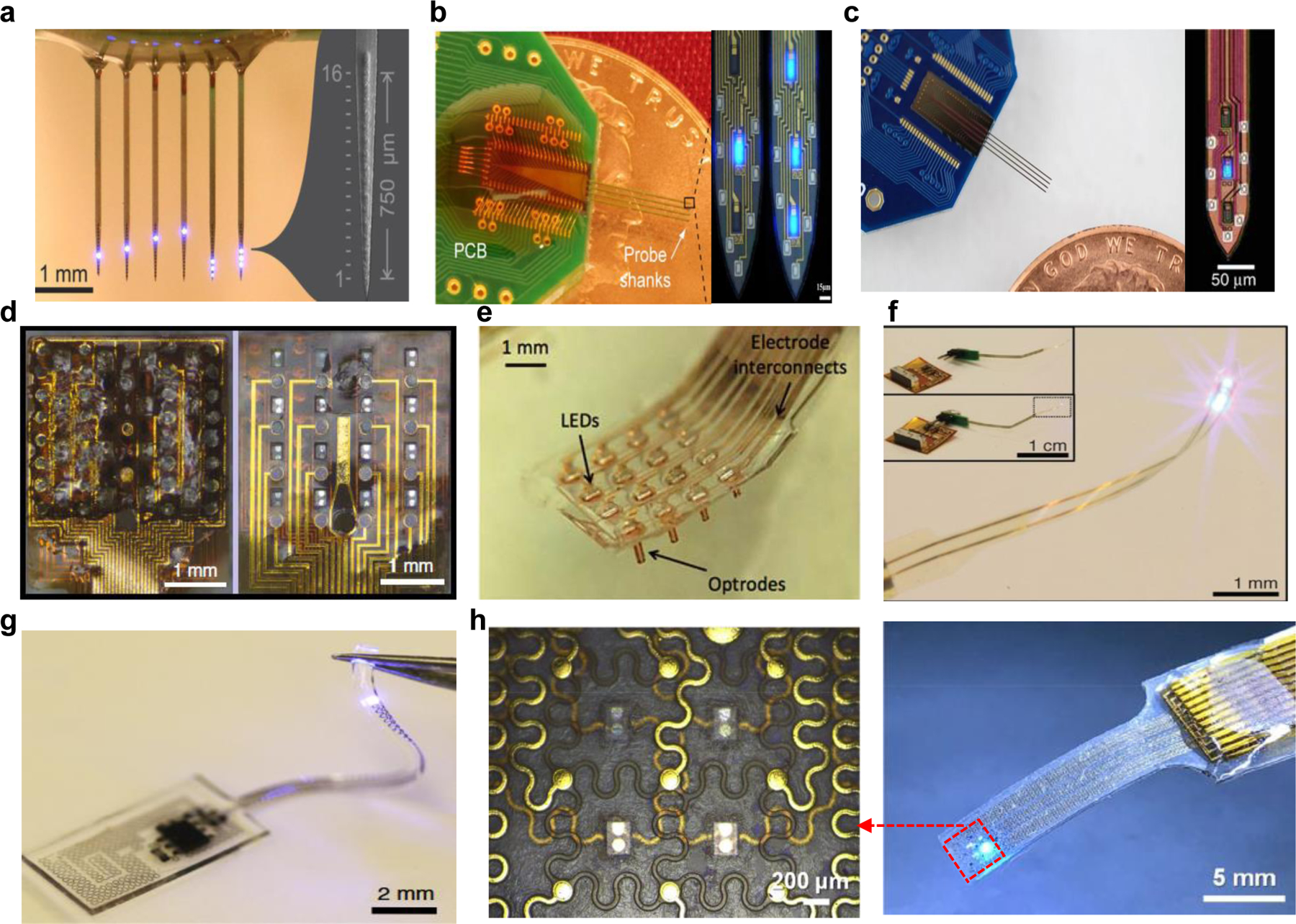
State-of-the-art neural probes/grids integrating electrodes and μ-LEDs. Stiff: (a) 6-shank μ-LED probe with 16 μ-LEDs per shank [126], (b) 4-shank probe with 3 μ-LEDs and 8 electrodes per shank [127], (c) Minimal-stimulation-artifact μ-LED optoelectrodes [128], Flexible: (d) The front side (left) and back side (right) of the flexible hybrid optoelectric neural interface based polyimide with 16 channels of both electrodes and μ-LEDs [148], (e) Probes array coupled with 16 μ-LEDs and 16 electrodes [149], (f) The ultra-flexible probe by the blue light-on μ-LED. The inset image display the integrated device concluding a wireless radio frequency scavenger [119], Stretchable: (g) soft, stretchable, fully implantable optoelectronic system integrated with μ-LEDs [152], and (h) Stretchable opto-electronic neural interface with 4 μ-LEDs and 9 recording electrodes (right) and schematic (left) [153].
4.2. Soft probes integrating electrodes and μ-LEDs
Having flexible or soft neural probes can alleviate micromotion-induced tissue damage [129–134]. While traditional silicon probes have been widely used, soft polymer materials are recently getting attention due to their flexibility and biocompatibility. For chemical sensing of the deep-brain and agent delivery, a flexible and multifunctional neural probe using liquid metal provided ultra large tunable stiffness [135]. There are several efforts on implantable flexible neural probes [122, 136–142], their biodegradable materials covering [143–147], and their usage in vivo validation.
Ji, et al. demonstrated a flexible PI-based hybrid optoelectric neural interface integrated with 16 μ-LEDs and 16-ch IrOx-modified electrodes (Fig. 3d) [148]. They showed stability of the device with 3-month soaking tests, and extensive research on thermal and electrochemical properties to show usefulness of this device for an optogenetic tool. Figure 3e presents a flexible probe array with multi-channel μ-LEDs and wireless-enabled, for bidirectional wireless neural interface [149]. For accurate delivery of light and recording of neural signals in multiple cortical layers altogether, the array integrated wirelessly addressable μ-LED chips with an inclined polymer probe array. In vivo tests on the brains of the rats found that the μ-LEDs could be powered inductively and controlled by utilizing a stimulator of wireless switched capacitor. A light induced neural activity was recorded simultaneously using integrated recording electrodes.
The development of the III-V compound semiconductor μ-LEDs enabled a dramatic improvement of optical and electrical performance compared to conventional LEDs due to their miniaturization [150]. Among many different compound semiconductors, GaN has a long history in LEDs to produce blue, violet, and ultra-violet (UV) laser diodes [151]. The major parameter of binary and ternary III-Nitride alloys is their bandgap energy value, which directly affects the output light wavelength on optoelectronic applications of the material. Figure 3f introduces a flexible, multifunctional, and wireless system, integrated with GaN-based μ-LEDs, having injectable capability [119]. In this work, ultra-small “cellular-scale” μ-LEDs with a size of 50 × 50 μm2 and thickness of 6.45 μm were utilized, having attenuated tissue damage, effective thermal management, and minimal inflammation for chronic uses. This multifunctional integrated system was mainly divided into four different layers, consisted of recording electrodes, photodetectors, μ-LEDs, and temperature sensors. This demonstration analyzed optical, thermal, and electrophysiological extensively, as well as chronic in vivo validation, including cell-type-specific expression of ChR2, electrical signal detection and real-time thermal sensing.
Utilizing elastomeric materials can create probes which are flexible and also remarkably softer, which can tolerate local stretching. Elastomeric probes are usually slightly thicker than flexible ones, but they have better mechanical compliance with the brain. A PDMS probe consisting of metallic structures with serpentine-shaped and off the shelf components along with embedded μ[issp]LEDs is fabricated (Fig. 3g) [152]. It is a soft optoelectronic neural system for wireless optogenetics, controlling different cells and field oscillations in mobile mice with a unique spatial resolution. Another stretchable optoelectronic neural interface was reported, having 4 μ-LEDs and 9 recording electrodes (Fig. 3h) [153]. This device used Dragonskin as substrate and encapsulation layers and incorporated serpentine-shaped interconnects for enhanced stretchability. They also successfully demonstrated ECoG signals with optogenetic stimulation of ChR2 from focal cortical areas of the awaked mouse in vivo recording.
In addition to optogenetic stimulation, implantable μ-LEDs can also be used for neural recording and imaging. Lee, et al. introduced an interesting approach combining the merits of electronics (CMOS for recording, signal amplification and encoding) and of optics (μ-LED for power and data uplink) by using microscale opto-electrically transduced electrodes (MOTEs) [154, 155]. These devices recorded in vivo neural activities in a tether-less fashion when implanted into the brain. While not demonstrated yet, MOTEs hold the potential to perform dual-modal optogenetic stimulation and electrical recording. Another example was an implantable single-photon imager integrated monolithically in the form of a complementary metal-oxide-semiconductor Integrated Circuit (CMOS IC) and optical image sensor array based on shank [156]. It could localize the fluorescent objects beyond conventional systems depth with a minimal tissue displacement. The other approach was an implantable lens-less, shank-based image sensor array and optical-filter-less allowing cellular-resolution recording at the arbitrary depths along with excitation which is provided by an outer laser light source [157].
Utilizing μ-LEDs can also realize three or more modalities (e.g., optical, chemical, fluidic, and electrical) integrated together by downscaling the component and developing creative fabrication methods with microfabricated polymer probes [86, 158]. These integrated systems often incorporate various tools and components, including implantable waveguides, control electronics, light sources, power supply, tools for implantation, and electrical interfaces [159]. Multiple components can be applied with microfabrication technology as a result of the small size of the μ-LEDs. Generally, combining optical and electrical techniques provides an exciting opportunity to examine the stimulation effect on organ-level activity. The combination of magnetic modality with both optogenetic stimulation and electrical recording to consider how optogenetic stimulation affects the extensive brain activities is another great approach [160]. This technique has recently been demonstrated as an effective tool to study depression and schizophrenia which are related to neural circuits in awake rats [161].
5. Conclusion and outlook
Neural interface with hybrid electrical-optical modalities consisted of new sets of circuits and sensors represents unique tools to understand the brain [162]. Especially, transparent electrodes allow simultaneous electrical recording and optical approaches especially imaging, converging complementary information on neuronal dimensions, types, and their activities. In addition to imaging, the invention and rapid development of optogenetics subsequently spurred the birth of a cohort of neural probes for light delivery, enabling cell-type-specific brain stimulation. Today, optical fiber-based probes are widely used in neuroscience studies, some even with compact and wireless devices for brain mapping. In parallel, hybrid probes with μ-LEDs have been developed significantly in the recent years, allowing optical stimulation with increased spatial resolution and stimulation with various wavelengths. Combining optical fibers or μ-LEDs with electrodes have therefore been enabling closed-loop interrogation of the brain and its underlying network. On the other hand, combining electrical and optical modalities could create new challenges where photo stimulation causes light-induced artifact due to photovoltaic effects that interfere with electrical signals from the brain. Great efforts have been made and will continuously be to reduce such artifacts by using different materials with low photovoltaic effects or developing new shielding strategies.
Looking ahead, a natural evolution of hybrid electrical-optical systems is also to scale up in a way that is minimally invasive. A variety of system functionalities, including signal multiplexing, data processing, signal digitalization, pattern recognition, and even data classification, may also be implanted in the brain altogether, permitting multipurpose interactions and reducing latency dramatically. Furthermore, the possibility of constructing hybrid electrical and optical systems on a chip still remains largely unexplored. Such an advanced hybrid system could greatly facilitate the acquisition of spatial data around the stimulation site and allow researchers to understand the area to area interaction and propagation of the brain signaling. Finally, it is also necessary to reduce the cost of manufacturing for widespread applications. Achieving these milestones will significantly advance fundamental neuroscience research as well as enable biomedical devices for clinical purposes.
Acknowledgement
This work is supported by National Science Foundation award 1847215, National Institute of Neurological Disorders and Stroke award 1RF1NS118301-01, and U.S. Army Medical Research Acquisition Activity award W81XWH-18-1-0699.
REFERENCES
- [1].Wellman SM, Eles JR, Ludwig KA, Seymour JP, Michelson NJ, McFadden WE, Vazquez AL and Kozai TD 2018. A materials roadmap to functional neural interface design Advanced functional materials 28 1701269. [DOI] [PMC free article] [PubMed] [Google Scholar]
- [2].Gupta P, Balasubramaniam N, Chang H-Y, Tseng F-G and Santra TS 2020. A Single-Neuron: Current Trends and Future Prospects Cells 9 1528. [DOI] [PMC free article] [PubMed] [Google Scholar]
- [3].Lago N and Cester A 2017. Flexible and organic neural interfaces: A review Applied Sciences 7 1292 [Google Scholar]
- [4].Ferguson M, Sharma D, Ross D and Zhao F 2019. A critical review of microelectrode arrays and strategies for improving neural interfaces Advanced healthcare materials 8 1900558. [DOI] [PMC free article] [PubMed] [Google Scholar]
- [5].Luan L, Robinson JT, Aazhang B, Chi T, Yang K, Li X, Rathore H, Singer A, Yellapantula S and Fan Y 2020. Recent Advances in Electrical Neural Interface Engineering: Minimal Invasiveness, Longevity, and Scalability Neuron 108 302–21 [DOI] [PMC free article] [PubMed] [Google Scholar]
- [6].Sotelo C 2003. Viewing the brain through the master hand of Ramon y Cajal Nature Reviews Neuroscience 4 71–7 [DOI] [PubMed] [Google Scholar]
- [7].Finkelstein G. Mechanical neuroscience: Emil du Bois-Reymond’s innovations in theory and practice. Frontiers in Systems Neuroscience. 2015;9 doi: 10.3389/fnsys.2015.00133. [DOI] [PMC free article] [PubMed] [Google Scholar]
- [8].Sherrington C 1952. The integrative action of the nervous system: CUP Archive; ) [Google Scholar]
- [9].Adrian ED and Matthews BH 1934. The interpretation of potential waves in the cortex The Journal of Physiology 81 440. [DOI] [PMC free article] [PubMed] [Google Scholar]
- [10].Naundorf B, Wolf F and Volgushev M 2006. Unique features of action potential initiation in cortical neurons Nature 440 1060–3 [DOI] [PubMed] [Google Scholar]
- [11].Häusser M 2000. The Hodgkin-Huxley theory of the action potential Nature Neuroscience 3 1165- [DOI] [PubMed] [Google Scholar]
- [12].Patil AC and Thakor NV 2016. Implantable neurotechnologies: a review of micro- and nanoelectrodes for neural recording Medical & Biological Engineering & Computing 54 23–44 [DOI] [PubMed] [Google Scholar]
- [13].Obaid SN, Chen Z and Lu L 2020. Advanced Electrical and Optical Microsystems for Biointerfacing Advanced Intelligent Systems 2 2000091 [Google Scholar]
- [14].Kozai TD, Jaquins-Gerstl AS, Vazquez AL, Michael AC and Cui XT 2015. Brain tissue responses to neural implants impact signal sensitivity and intervention strategies ACS chemical neuroscience 6 48–67 [DOI] [PMC free article] [PubMed] [Google Scholar]
- [15].Sommakia S, Lee HC, Gaire J and Otto KJ 2014. Materials approaches for modulating neural tissue responses to implanted microelectrodes through mechanical and biochemical means Current Opinion in Solid State and Materials Science 18 319–28 [DOI] [PMC free article] [PubMed] [Google Scholar]
- [16].Tsodyks M, Kenet T, Grinvald A and Arieli A 1999. Linking spontaneous activity of single cortical neurons and the underlying functional architecture Science 286 1943–6 [DOI] [PubMed] [Google Scholar]
- [17].Goncalves SB, Ribeiro JF, Silva AF, Costa RM and Correia JH 2017. Design and manufacturing challenges of optogenetic neural interfaces: a review Journal of Neural Engineering 14 041001. [DOI] [PubMed] [Google Scholar]
- [18].Pisano F, Zampaglione E, McAlinden N, Roebber J, Dawson MD, Mathieson K and Sher A 2017. Large scale matching of function to the genetic identity of retinal ganglion cells Scientific reports 7 1–12 [DOI] [PMC free article] [PubMed] [Google Scholar]
- [19].Mahmoudi P, Veladi H and Pakdel FG 2017. Optogenetics, tools and applications in neurobiology Journal of medical signals and sensors 7 71. [PMC free article] [PubMed] [Google Scholar]
- [20].Zhao H. Recent progress of development of optogenetic implantable neural probes. International journal of molecular sciences. 2017;18:1751. doi: 10.3390/ijms18081751. [DOI] [PMC free article] [PubMed] [Google Scholar]
- [21].Govorunova EG, Sineshchekov OA, Li H and Spudich JL 2017. Microbial Rhodopsins: Diversity, Mechanisms, and Optogenetic Applications Annual Review of Biochemistry 86 845–72 [DOI] [PMC free article] [PubMed] [Google Scholar]
- [22].Canales A, Park S, Kilias A and Anikeeva P 2018. Multifunctional fibers as tools for neuroscience and neuroengineering Accounts of Chemical Research 51 829–38 [DOI] [PubMed] [Google Scholar]
- [23].Nazempour R, Zhang Q, Fu R and Sheng X 2018. Biocompatible and Implantable Optical Fibers and Waveguides for Biomedicine Materials 11 [DOI] [PMC free article] [PubMed] [Google Scholar]
- [24].Seo KJ, Qiang Y, Bilgin I, Kar S, Vinegoni C, Weissleder R and Fang H 2017. Transparent electrophysiology microelectrodes and interconnects from metal nanomesh ACS nano 11 436572. [DOI] [PubMed] [Google Scholar]
- [25].Schendel AA, Thongpang S, Brodnick SK, Richner TJ, Lindevig BDB, Krugner-Higby L and Williams JC 2013. A cranial window imaging method for monitoring vascular growth around chronically implanted micro-ECoG devices Journal of Neuroscience Methods 218 121–30 [DOI] [PMC free article] [PubMed] [Google Scholar]
- [26].Ledochowitsch P, Olivero E, Blanche T and Maharbiz MM 2011. A transparent μECoG array for simultaneous recording and optogenetic stimulation. In: 2011 Annual International Conference of the IEEE Engineering in Medicine and Biology Society: IEEE) pp 2937–40 [DOI] [PubMed] [Google Scholar]
- [27].Kuppusami S and Oskouei RH 2015. Parylene coatings in medical devices and implants: A review Univ. J. Biomed. Eng 3 9–14 [Google Scholar]
- [28].Paetzold R, Heuser K, Henseler D, Roeger S, Wittmann G and Winnacker A 2003. Performance of flexible polymeric light-emitting diodes under bending conditions Applied physics letters 82 33424 [Google Scholar]
- [29].Kwon KY, Sirowatka B, Weber A and Li W 2013. Opto-μECoG Array: A Hybrid Neural Interface With Transparent μECoG Electrode Array and Integrated LEDs for Optogenetics IEEE Transactions on Biomedical Circuits and Systems 7 593–600 [DOI] [PubMed] [Google Scholar]
- [30].Zátonyi A, Madarász M, Szabó Á, Lőrincz T, Hodován R, Rózsa B and Fekete Z 2020. Transparent, low-autofluorescence microECoG device for simultaneous Ca2+imaging and cortical electrophysiologyin vivo Journal of Neural Engineering 17 016062. [DOI] [PubMed] [Google Scholar]
- [31].Gautam V, Drury J, Choy JMC, Stricker C, Bachor H-A and Daria VR 2015. Improved two-photon imaging of living neurons in brain tissue through temporal gating Biomedical Optics Express 6 4027–36 [DOI] [PMC free article] [PubMed] [Google Scholar]
- [32].Lee J, Ozden I, Song Y-K and Nurmikko AV 2015. Transparent intracortical microprobe array for simultaneous spatiotemporal optical stimulation and multichannel electrical recording Nature methods 12 1157–62 [DOI] [PubMed] [Google Scholar]
- [33].Geim AK and Novoselov KS 2010. Nanoscience and technology: a collection of reviews from nature journals: World Scientific; ) pp 11–9 [Google Scholar]
- [34].Lee C, Wei X, Kysar JW and Hone J 2008. Measurement of the Elastic Properties and Intrinsic Strength of Monolayer Graphene, Science 321 385. [DOI] [PubMed] [Google Scholar]
- [35].Park D-W, Schendel AA, Mikael S, Brodnick SK, Richner TJ, Ness JP, Hayat MR, Atry F, Frye ST, Pashaie R, Thongpang S, Ma Z and Williams JC 2014. Graphene-based carbon-layered electrode array technology for neural imaging and optogenetic applications Nature Communications 5 5258. [DOI] [PMC free article] [PubMed] [Google Scholar]
- [36].Kuzum D, Takano H, Shim E, Reed JC, Juul H, Richardson AG, de Vries J, Bink H, Dichter MA, Lucas TH, Coulter DA, Cubukcu E and Litt B 2014. Transparent and flexible low noise graphene electrodes for simultaneous electrophysiology and neuroimaging Nature Communications 5 5259. [DOI] [PMC free article] [PubMed] [Google Scholar]
- [37].Thunemann M, Lu Y, Liu X, Kılıç K, Desjardins M, Vandenberghe M, Sadegh S, Saisan PA, Cheng Q and Weldy KL 2018. Deep 2-photon imaging and artifact-free optogenetics through transparent graphene microelectrode arrays Nature communications 9 1–12 [DOI] [PMC free article] [PubMed] [Google Scholar]
- [38].Vinnikova S, Fang H and Wang S 2020. Mechanics of Regular-Shape Nanomeshes for Transparent and Stretchable Devices Journal of Applied Mechanics 87 [Google Scholar]
- [39].Qiang Y, Seo KJ, Zhao X, Artoni P, Golshan NH, Culaclii S, Wang PM, Liu W, Ziemer KS and Fagiolini M 2017. Bilayer nanomesh structures for transparent recording and stimulating microelectrodes Advanced Functional Materials 27 1704117 [Google Scholar]
- [40].Qiang Y, Artoni P, Seo KJ, Culaclii S, Hogan V, Zhao X, Zhong Y, Han X, Wang P-M, Lo Y-K, Li Y, Patel HA, Huang Y, Sambangi A, Chu JSV, Liu W, Fagiolini M and Fang H 2018. Transparent arrays of bilayer-nanomesh microelectrodes for simultaneous electrophysiology and two-photon imaging in the brain Science Advances 4 eaat0626. [DOI] [PMC free article] [PubMed] [Google Scholar]
- [41].Seo KJ, Artoni P, Qiang Y, Zhong Y, Han X, Shi Z, Yao W, Fagiolini M and Fang H 2019. Transparent, Flexible, Penetrating Microelectrode Arrays with Capabilities of Single-Unit Electrophysiology Advanced Biosystems 3 1800276. [DOI] [PubMed] [Google Scholar]
- [42].Renz AF, Lee J, Tybrandt K, Brzezinski M, Lorenzo DA, Cerra Cheraka M, Lee J, Helmchen F, Vörös J and Lewis CM 2020. Opto-E-Dura: A Soft, Stretchable ECoG Array for Multimodal, Multiscale Neuroscience Advanced healthcare materials 9 2000814. [DOI] [PubMed] [Google Scholar]
- [43].Neto JP, Costa A, Pinto JV, Marques–Smith A, Costa J, Martins R, Fortunato E, Kampff A and Barquinha P 2020. Transparent and flexible ECoG electrode arrays based on silver nanowire networks for neural recordings bioRxiv 2020.02.24.962878 [Google Scholar]
- [44].Seo JW, Kim K, Seo KW, Kim MK, Jeong S, Kim H, Ghim JW, Lee JH, Choi N and Lee JY 2020. Artifact-Free 2D Mapping of Neural Activity In Vivo through Transparent Gold Nanonetwork Array Advanced Functional Materials 30 2000896 [Google Scholar]
- [45].Lee W, Kim D, Matsuhisa N, Nagase M, Sekino M, Malliaras GG, Yokota T and Someya T 2017. Transparent, conformable, active multielectrode array using organic electrochemical transistors Proceedings of the National Academy of Sciences 114 10554. [DOI] [PMC free article] [PubMed] [Google Scholar]
- [46].Alwis L, Sun T and Grattan K 2016. Developments in optical fibre sensors for industrial applications Optics & Laser Technology 78 62–6 [Google Scholar]
- [47].HOPKINS HH and Kapany NS 1954. A flexible fibrescope, using static scanning Nature 173 39–41 [Google Scholar]
- [48].Cheng S-F and Chau L-K 2003. Colloidal gold-modified optical fiber for chemical and biochemical sensing Analytical chemistry 75 16–21 [DOI] [PubMed] [Google Scholar]
- [49].Mowbray SE and Amiri AM 2019. A brief overview of medical fiber optic biosensors and techniques in the modification for enhanced sensing ability Diagnostics 9 23. [DOI] [PMC free article] [PubMed] [Google Scholar]
- [50].Patel AA, McAlinden N, Mathieson K and Sakata S 2020. Simultaneous electrophysiology and fiber photometry in freely behaving mice Frontiers in neuroscience 14 148. [DOI] [PMC free article] [PubMed] [Google Scholar]
- [51].Sych Y, Chernysheva M, Sumanovski LT and Helmchen F 2019. High-density multi-fiber photometry for studying large-scale brain circuit dynamics Nature methods 16 553. [DOI] [PubMed] [Google Scholar]
- [52].Lu L, Gutruf P, Xia L, Bhatti DL, Wang X, Vazquez-Guardado A, Ning X, Shen X, Sang T and Ma R 2018. Wireless optoelectronic photometers for monitoring neuronal dynamics in the deep brain Proceedings of the National Academy of Sciences 115 E1374–E83 [DOI] [PMC free article] [PubMed] [Google Scholar]
- [53].Levene MJ, Dombeck DA, Kasischke KA, Molloy RP and Webb WW 2004. In vivo multiphoton microscopy of deep brain tissue Journal of neurophysiology 91 1908–12 [DOI] [PubMed] [Google Scholar]
- [54].Adams JK, Boominathan V, Avants BW, Vercosa DG, Ye F, Baraniuk RG, Robinson JT and Veeraraghavan A 2017. Single-frame 3D fluorescence microscopy with ultraminiature lensless FlatScope Science advances 3 e1701548. [DOI] [PMC free article] [PubMed] [Google Scholar]
- [55].Zorzos AN, Boyden ES and Fonstad CG 2010. Multiwaveguide implantable probe for light delivery to sets of distributed brain targets Optics letters 35 4133–5 [DOI] [PMC free article] [PubMed] [Google Scholar]
- [56].Abaya T, Blair S, Tathireddy P, Rieth L and Solzbacher F 2012. A 3D glass optrode array for optical neural stimulation Biomedical optics express 3 3087–104 [DOI] [PMC free article] [PubMed] [Google Scholar]
- [57].Zorzos AN, Scholvin J, Boyden ES and Fonstad CG 2012. Three-dimensional multiwaveguide probe array for light delivery to distributed brain circuits Optics letters 37 4841–3 [DOI] [PMC free article] [PubMed] [Google Scholar]
- [58].Pisanello F, Mandelbaum G, Pisanello M, Oldenburg IA, Sileo L, Markowitz JE, Peterson RE, Della Patria A, Haynes TM and Emara MS 2017. Dynamic illumination of spatially restricted or large brain volumes via a single tapered optical fiber Nature neuroscience 20 1180–8 [DOI] [PMC free article] [PubMed] [Google Scholar]
- [59].Davey CJ, Argyros A, Fleming SC and Solomon SG 2015. Multimodal optogenetic neural interfacing device fabricated by scalable optical fiber drawing technique Applied Optics 54 10068–72 [DOI] [PubMed] [Google Scholar]
- [60].Wu F, Stark E, Im M, Cho I-J, Yoon E-S, Buzsáki G, Wise KD and Yoon E 2013. An implantable neural probe with monolithically integrated dielectric waveguide and recording electrodes for optogenetics applications J Neural Eng 10 056012. [DOI] [PMC free article] [PubMed] [Google Scholar]
- [61].Dufour S, Lavertu G, Dufour-Beauséjour S, Juneau-Fecteau A, Calakos N, Deschênes M, Vallée R and De Koninck Y 2013. A multimodal micro-optrode combining field and single unit recording, multispectral detection and photolabeling capabilities PloS one 8 e57703. [DOI] [PMC free article] [PubMed] [Google Scholar]
- [62].LeChasseur Y, Dufour S, Lavertu G, Bories C, Deschênes M, Vallée R and De Koninck Y 2011. A microprobe for parallel optical and electrical recordings from single neurons in vivo Nature methods 8 319–25 [DOI] [PubMed] [Google Scholar]
- [63].Park S, Loke G, Fink Y and Anikeeva P 2019. Flexible fiber-based optoelectronics for neural interfaces Chemical Society Reviews 48 1826–52 [DOI] [PubMed] [Google Scholar]
- [64].Sridharan A, Rajan SD and Muthuswamy J 2013. Long-term changes in the material properties of brain tissue at the implant–tissue interface Journal of neural engineering 10 066001. [DOI] [PMC free article] [PubMed] [Google Scholar]
- [65].Gilletti A and Muthuswamy J 2006. Brain micromotion around implants in the rodent somatosensory cortex Journal of neural engineering 3 189. [DOI] [PubMed] [Google Scholar]
- [66].Lee H, Bellamkonda RV, Sun W and Levenston ME 2005. Biomechanical analysis of silicon microelectrode-induced strain in the brain J Neural Eng 2 81. [DOI] [PubMed] [Google Scholar]
- [67].Zubia J and Arrue J 2001. Plastic optical fibers: An introduction to their technological processes and applications Optical fiber technology 7 101–40 [Google Scholar]
- [68].Sanghera J and Aggarwal I 1999. Active and passive chalcogenide glass optical fibers for IR applications: a review Journal of Non-Crystalline Solids 256 6–16 [Google Scholar]
- [69].Nielsen K, Rasmussen HK, Adam AJ, Planken PC, Bang O and Jepsen PU 2009. Bendable, low-loss Topas fibers for the terahertz frequency range Optics Express 17 8592–601 [DOI] [PubMed] [Google Scholar]
- [70].Khanarian G 2001. Optical properties of cyclic olefin copolymers Optical Engineering 40 1024–30 [Google Scholar]
- [71].Iftekhar S, Grins J and Edén M 2010. Composition–property relationships of the La2O3–Al2O3–SiO2 glass system Journal of non-crystalline solids 356 1043–8 [Google Scholar]
- [72].Sheeba M 2008. Fabrication and Characterization of Polymer Optical Fibers for Photonic Device Applications. Citeseer) [Google Scholar]
- [73].Fu R, Luo W, Nazempour R, Tan D, Ding H, Zhang K, Yin L, Guan J and Sheng X 2018. Implantable and Biodegradable Poly (l‐lactic acid) Fibers for Optical Neural Interfaces, Advanced Optical Materials 6 1700941 [Google Scholar]
- [74].Nazempour R, Zhang Q, Fu R and Sheng X 2018. Biocompatible and implantable optical fibers and waveguides for biomedicine Materials 11 1283. [DOI] [PMC free article] [PubMed] [Google Scholar]
- [75].Luo Y, Yan B, Zhang Q, Peng G-D, Wen J and Zhang J 2017. Fabrication of polymer optical fibre (POF) gratings Sensors 17 511. [DOI] [PMC free article] [PubMed] [Google Scholar]
- [76].Shukla S, Kushwaha CS, Guner T and Demir MM 2019. Chemically modified optical fibers in advanced technology: An overview Optics & Laser Technology 115 404–32 [Google Scholar]
- [77].Stajanca P, Topolniak I, Pötschke S and Krebber K 2018. Solution-mediated cladding doping of commercial polymer optical fibers Optical Fiber Technology 41 227–34 [Google Scholar]
- [78].Tyler DR 2004. Mechanistic aspects of the effects of stress on the rates of photochemical degradation reactions in polymers Journal of Macromolecular Science, Part C: Polymer Reviews 44 351–88 [Google Scholar]
- [79].Blanc W and Dussardier B 2016. Formation and applications of nanoparticles in silica optical fibers Journal of Optics 45 247–54 [Google Scholar]
- [80].Yan W, Dong C, Xiang Y, Jiang S, Leber A, Loke G, Xu W, Hou C, Zhou S and Chen M 2020. Thermally drawn advanced functional fibers: New frontier of flexible electronics Materials Today [Google Scholar]
- [81].Bayindir M, Sorin F, Abouraddy AF, Viens J, Hart SD, Joannopoulos JD and Fink Y 2004. Metal–insulator–semiconductor optoelectronic fibres Nature 431 826–9 [DOI] [PubMed] [Google Scholar]
- [82].Resendez SL and Stuber GD 2015. In vivo calcium imaging to illuminate neurocircuit activity dynamics underlying naturalistic behavior Neuropsychopharmacology 40 238. [DOI] [PMC free article] [PubMed] [Google Scholar]
- [83].Guo Q, Zhou J, Feng Q, Lin R, Gong H, Luo Q, Zeng S, Luo M and Fu L 2015. Multi-channel fiber photometry for population neuronal activity recording Biomedical optics express 6 3919–31 [DOI] [PMC free article] [PubMed] [Google Scholar]
- [84].Stolyarov AM, Gumennik A, McDaniel W, Shapira O, Schell B, Sorin F, Kuriki K, Benoit G, Rose A and Joannopoulos JD 2012. Enhanced chemiluminescent detection scheme for trace vapor sensing in pneumatically-tuned hollow core photonic bandgap fibers Optics Express 20 12407–15 [DOI] [PubMed] [Google Scholar]
- [85].Khudiyev T, Clayton J, Levy E, Chocat N, Gumennik A, Stolyarov AM, Joannopoulos J and Fink Y 2017. Electrostrictive microelectromechanical fibres and textiles Nature communications 8 1–7 [DOI] [PMC free article] [PubMed] [Google Scholar]
- [86].Canales A, Jia X, Froriep UP, Koppes RA, Tringides CM, Selvidge J, Lu C, Hou C, Wei L and Fink Y 2015. Multifunctional fibers for simultaneous optical, electrical and chemical interrogation of neural circuits in vivo Nature biotechnology 33 277–84 [DOI] [PubMed] [Google Scholar]
- [87].Park S, Guo Y, Jia X, Choe HK, Grena B, Kang J, Park J, Lu C, Canales A and Chen R 2017. One-step optogenetics with multifunctional flexible polymer fibers Nature neuroscience 20 612–9 [DOI] [PMC free article] [PubMed] [Google Scholar]
- [88].Lu C, Park S, Richner TJ, Derry A, Brown I, Hou C, Rao S, Kang J, Moritz CT and Fink Y 2017. Flexible and stretchable nanowire-coated fibers for optoelectronic probing of spinal cord circuits Science advances 3 e1600955. [DOI] [PMC free article] [PubMed] [Google Scholar]
- [89].Zhang J, Laiwalla F, Kim JA, Urabe H, Van Wagenen R, Song Y-K, Connors BW, Zhang F, Deisseroth K and Nurmikko AV 2009. Integrated device for optical stimulation and spatiotemporal electrical recording of neural activity in light-sensitized brain tissue J Neural Eng 6 055007. [DOI] [PMC free article] [PubMed] [Google Scholar]
- [90].Bernstein JG, Allen BD, Guerra AA and Boyden ES 2015. Processes for design, construction and utilisation of arrays of light-emitting diodes and light-emitting diode-coupled optical fibres for multi-site brain light delivery Journal of engineering (Stevenage, England) 2015 [DOI] [PMC free article] [PubMed] [Google Scholar]
- [91].Stark E, Koos T and Buzsáki G 2012. Diode probes for spatiotemporal optical control of multiple neurons in freely moving animals Journal of neurophysiology 108 349–63 [DOI] [PMC free article] [PubMed] [Google Scholar]
- [92].Royer S, Zemelman BV, Barbic M, Losonczy A, Buzsáki G and Magee JC 2010. Multi‐array silicon probes with integrated optical fibers: light‐assisted perturbation and recording of local neural circuits in the behaving animal European Journal of Neuroscience 31 2279–91 [DOI] [PMC free article] [PubMed] [Google Scholar]
- [93].Tamura K, Ohashi Y, Tsubota T, Takeuchi D, Hirabayashi T, Yaguchi M, Matsuyama M, Sekine T and Miyashita Y 2012. A glass-coated tungsten microelectrode enclosing optical fibers for optogenetic exploration in primate deep brain structures Journal of neuroscience methods 211 49–57 [DOI] [PubMed] [Google Scholar]
- [94].Park H, Shin H-J, Cho I-J, Yoon E-s, Suh J-KF, Im M, Yoon E, Kim Y-J and Kim J 2011. The first neural probe integrated with light source (blue laser diode) for optical stimulation and electrical recording. In: 2011 Annual International Conference of the IEEE Engineering in Medicine and Biology Society: IEEE) pp 2961–4 [DOI] [PubMed] [Google Scholar]
- [95].Chen S, Pei W, Gui Q, Chen Y, Zhao S, Wang H and Chen H 2013. A fiber-based implantable multi-optrode array with contiguous optical and electrical sites Journal of neural engineering 10 046020. [DOI] [PubMed] [Google Scholar]
- [96].Aravanis AM, Wang L-P, Zhang F, Meltzer LA, Mogri MZ, Schneider MB and Deisseroth K 2007. An optical neural interface: in vivo control of rodent motor cortex with integrated fiberoptic and optogenetic technology Journal of neural engineering 4 S143. [DOI] [PubMed] [Google Scholar]
- [97].Bernstein JG, Han X, Henninger MA, Ko EY, Qian X, Franzesi GT, McConnell JP, Stern P, Desimone R and Boyden ES 2008. Prosthetic systems for therapeutic optical activation and silencing of genetically targeted neurons. In: Optical Interactions with Tissue and Cells XIX: International Society for Optics and Photonics; ) p 68540H. [DOI] [PMC free article] [PubMed] [Google Scholar]
- [98].Schwaerzle M, Elmlinger P, Paul O and Ruther P 2015. Miniaturized 3× 3 optical fiber array for optogenetics with integrated 460 nm light sources and flexible electrical interconnection. In: 2015 28th IEEE International Conference on Micro Electro Mechanical Systems (MEMS): IEEE) pp 162–5 [Google Scholar]
- [99].Ozden I, Wang J, Lu Y, May T, Lee J, Goo W, O’Shea DJ, Kalanithi P, Diester I and Diagne M 2013. A coaxial optrode as multifunction write-read probe for optogenetic studies in non-human primates Journal of neuroscience methods 219 142–54 [DOI] [PMC free article] [PubMed] [Google Scholar]
- [100].Duffy BA, Choy M, Chuapoco MR, Madsen M and Lee JH 2015. MRI compatible optrodes for simultaneous LFP and optogenetic fMRI investigation of seizure-like afterdischarges Neuroimage 123 173–84 [DOI] [PMC free article] [PubMed] [Google Scholar]
- [101].Voigts J, Siegle JH, Pritchett DL and Moore CI 2013. The flexDrive: an ultra-light implant for optical control and highly parallel chronic recording of neuronal ensembles in freely moving mice Frontiers in systems neuroscience 7 8. [DOI] [PMC free article] [PubMed] [Google Scholar]
- [102].Pisanello F, Sileo L, Oldenburg IA, Pisanello M, Martiradonna L, Assad JA, Sabatini BL and De Vittorio M 2014. Multipoint-emitting optical fibers for spatially addressable in vivo optogenetics Neuron 82 1245–54 [DOI] [PMC free article] [PubMed] [Google Scholar]
- [103].Wang J, Wagner F, Borton DA, Zhang J, Ozden I, Burwell RD, Nurmikko AV, van Wagenen R, Diester I and Deisseroth K 2011. Integrated device for combined optical neuromodulation and electrical recording for chronic in vivo applications J Neural Eng 9 016001. [DOI] [PubMed] [Google Scholar]
- [104].Guo S, Zhou H, Zhang J, Xu K and Zheng X 2013. A multi-electrode array coupled with fiberoptic for deep-brain optical neuromodulation and electrical recording. In: 2013 35th Annual International Conference of the IEEE Engineering in Medicine and Biology Society (EMBC): IEEE) pp 2752–5 [DOI] [PubMed] [Google Scholar]
- [105].Sparta DR, Stamatakis AM, Phillips JL, Hovelsø N, Van Zessen R and Stuber GD 2012. Construction of implantable optical fibers for long-term optogenetic manipulation of neural circuits Nature protocols 7 12–23 [DOI] [PMC free article] [PubMed] [Google Scholar]
- [106].Sileo L, Bitzenhofer SH, Spagnolo B, Pöpplau JA, Holzhammer T, Pisanello M, Pisano F, Bellistri E, Maglie E and De Vittorio M 2018. Tapered fibers combined with a multi-electrode array for optogenetics in mouse medial prefrontal cortex Frontiers in neuroscience 12 771. [DOI] [PMC free article] [PubMed] [Google Scholar]
- [107].Parker ST, Domachuk P, Amsden J, Bressner J, Lewis JA, Kaplan DL and Omenetto FG 2009. Biocompatible silk printed optical waveguides Advanced Materials 21 2411–5 [Google Scholar]
- [108].Jain A, Yang AH and Erickson D 2012. Gel-based optical waveguides with live cell encapsulation and integrated microfluidics Optics letters 37 1472–4 [DOI] [PubMed] [Google Scholar]
- [109].Orf ND, Shapira O, Sorin F, Danto S, Baldo MA, Joannopoulos JD and Fink Y 2011. Fiber draw synthesis Proceedings of the National Academy of Sciences 108 4743–7 [Google Scholar]
- [110].Abouraddy A, Bayindir M, Benoit G, Hart S, Kuriki K, Orf N, Shapira O, Sorin F, Temelkuran B and Fink Y 2007. Towards multimaterial multifunctional fibres that see, hear, sense and communicate Nature materials 6 336–47 [DOI] [PubMed] [Google Scholar]
- [111].Canales A, Jia X, Lu C, Froriep UP, Koppes RA, Tringides CM, Selvidge J, Fink Y and Anikeeva P 2015. Optoelectronic Probing of Neural Circuits with Multifunctional Fibers. In: Optics and the Brain: Optical Society of America; ) p BrT4B. 2 [DOI] [PubMed] [Google Scholar]
- [112].Xu H, Davitt KM, Dong W, Song Y-K, Patterson WR III, Aizenman CD and Nurmikko AV 2008. Combining multicore imaging fiber with matrix addressable blue/green LED arrays for spatiotemporal photonic excitation at cellular level IEEE Journal of Selected Topics in Quantum Electronics 14 167–70 [Google Scholar]
- [113].Hayashi Y, Tagawa Y, Yawata S, Nakanishi S and Funabiki K 2012. Spatio‐temporal control of neural activity in vivo using fluorescence microendoscopy European Journal of Neuroscience 36 2722–32 [DOI] [PubMed] [Google Scholar]
- [114].Rivnay J, Wang H, Fenno L, Deisseroth K and Malliaras GG 2017. Next-generation probes, particles, and proteins for neural interfacing Science Advances 3 e1601649. [DOI] [PMC free article] [PubMed] [Google Scholar]
- [115].Gradinaru V, Thompson KR, Zhang F, Mogri M, Kay K, Schneider MB and Deisseroth K 2007. Targeting and readout strategies for fast optical neural control in vitro and in vivo Journal of Neuroscience 27 14231–8 [DOI] [PMC free article] [PubMed] [Google Scholar]
- [116].Wang L, Huang K, Zhong C, Wang L and Lu Y 2018. Fabrication and modification of implantable optrode arrays for in vivo optogenetic applications Biophysics reports 4 82–93 [DOI] [PMC free article] [PubMed] [Google Scholar]
- [117].Yoo S, Lee H, Jun SB, Kim Y-K and Ji C-H 2018. Disposable MEMS optrode array integrated with single LED for neurostimulation Sensors and Actuators A: Physical 273 276–84 [Google Scholar]
- [118].Campbell PK, Jones KE, Huber RJ, Horch KW and Normann RA 1991. A silicon-based, three-dimensional neural interface: manufacturing processes for an intracortical electrode array IEEE Transactions on Biomedical Engineering 38 758–68 [DOI] [PubMed] [Google Scholar]
- [119].Kim T-i, McCall JG, Jung YH, Huang X, Siuda ER, Li Y, Song J, Song YM, Pao HA and Kim R-H 2013. Injectable, cellular-scale optoelectronics with applications for wireless optogenetics Science 340 211–6 [DOI] [PMC free article] [PubMed] [Google Scholar]
- [120].Kuzum D, Takano H, Shim E, Reed JC, Juul H, Richardson AG, De Vries J, Bink H, Dichter MA and Lucas TH 2014. Transparent and flexible low noise graphene electrodes for simultaneous electrophysiology and neuroimaging Nature communications 5 1–10 [DOI] [PMC free article] [PubMed] [Google Scholar]
- [121].Park D-W, Schendel AA, Mikael S, Brodnick SK, Richner TJ, Ness JP, Hayat MR, Atry F, Frye ST and Pashaie R 2014. Graphene-based carbon-layered electrode array technology for neural imaging and optogenetic applications Nature communications 5 1–11 [DOI] [PMC free article] [PubMed] [Google Scholar]
- [122].McCall JG, Kim T-i, Shin G, Huang X, Jung YH, Al-Hasani R, Omenetto FG, Bruchas MR and Rogers JA 2013. Fabrication and application of flexible, multimodal light-emitting devices for wireless optogenetics Nature protocols 8 2413. [DOI] [PMC free article] [PubMed] [Google Scholar]
- [123].Lee ST, Williams PA, Braine CE, Lin D-T, John SW and Irazoqui PP 2015. A miniature, fiber-coupled, wireless, deep-brain optogenetic stimulator IEEE Transactions on Neural Systems and Rehabilitation Engineering 23 655–64 [DOI] [PubMed] [Google Scholar]
- [124].Iwai Y, Honda S, Ozeki H, Hashimoto M and Hirase H 2011. A simple head-mountable LED device for chronic stimulation of optogenetic molecules in freely moving mice Neuroscience research 70 124–7 [DOI] [PubMed] [Google Scholar]
- [125].Wentz CT, Bernstein JG, Monahan P, Guerra A, Rodriguez A and Boyden ES 2011. A wirelessly powered and controlled device for optical neural control of freely-behaving animals Journal of neural engineering 8 046021. [DOI] [PMC free article] [PubMed] [Google Scholar]
- [126].Scharf R, Tsunematsu T, McAlinden N, Dawson MD, Sakata S and Mathieson K 2016. Depth-specific optogenetic control in vivo with a scalable, high-density μLED neural probe Scientific reports 6 28381. [DOI] [PMC free article] [PubMed] [Google Scholar]
- [127].Wu F, Stark E, Ku P-C, Wise KD, Buzsáki G and Yoon E 2015. Monolithically integrated μLEDs on silicon neural probes for high-resolution optogenetic studies in behaving animals Neuron 88 113648. [DOI] [PMC free article] [PubMed] [Google Scholar]
- [128].Kim K, Vöröslakos M, Seymour JP, Wise KD, Buzsáki G and Yoon E 2020. Artifact-free and high-temporal-resolution in vivo opto-electrophysiology with microLED optoelectrodes Nature communications 11 1–12 [DOI] [PMC free article] [PubMed] [Google Scholar]
- [129].Rousche PJ, Pellinen DS, Pivin DP, Williams JC, Vetter RJ and Kipke DR 2001. Flexible polyimide-based intracortical electrode arrays with bioactive capability Ieee T Bio-Med Eng 48 361–71 [DOI] [PubMed] [Google Scholar]
- [130].Xiang Z, Yen S-C, Xue N, Sun T, Tsang WM, Zhang S, Liao L-D, Thakor NV and Lee C 2014. Ultrathin flexible polyimide neural probe embedded in a dissolvable maltose-coated microneedle Journal of Micromechanics and Microengineering 24 065015 [Google Scholar]
- [131].Stieglitz T 2001. Flexible biomedical microdevices with double-sided electrode arrangements for neural applications Sensors and Actuators A: Physical 90 203–11 [Google Scholar]
- [132].Tooker A, Tolosa V, Shah KG, Sheth H, Felix S, Delima T and Pannu S 2012. Polymer neural interface with dual-sided electrodes for neural stimulation and recording. In: 2012 Annual International Conference of the IEEE Engineering in Medicine and Biology Society: IEEE) pp 5999–6002 [DOI] [PubMed] [Google Scholar]
- [133].Minev IR, Musienko P, Hirsch A, Barraud Q, Wenger N, Moraud EM, Gandar J, Capogrosso M, Milekovic T, Asboth L, Torres RF, Vachicouras N, Liu Q, Pavlova N, Duis S, Larmagnac A, Vörös J, Micera S, Suo Z, Courtine G and Lacour SP 2015. Electronic dura mater for long-term multimodal neural interfaces Science 347 159–63 [DOI] [PubMed] [Google Scholar]
- [134].Lee K-K, He J, Singh A, Massia S, Ehteshami G, Kim B and Raupp G 2003. Polyimide-based intracortical neural implant with improved structural stiffness Journal of Micromechanics and Microengineering 14 32 [Google Scholar]
- [135].Wen X, Wang B, Huang S, Lee M-S, Chung P-S, Chow YT, Huang I-W, Monbouquette HG, Maidment NT and Chiou P-Y 2019. Flexible, multifunctional neural probe with liquid metal enabled, ultra-large tunable stiffness for deep-brain chemical sensing and agent delivery Biosensors and Bioelectronics 131 37–45 [DOI] [PMC free article] [PubMed] [Google Scholar]
- [136].Woeppel K, Yang Q and Cui XT 2017. Recent advances in neural electrode–tissue interfaces Current opinion in biomedical engineering 4 21–31 [DOI] [PMC free article] [PubMed] [Google Scholar]
- [137].Kozai TDY, Langhals NB, Patel PR, Deng X, Zhang H, Smith KL, Lahann J, Kotov NA and Kipke DR 2012. Ultrasmall implantable composite microelectrodes with bioactive surfaces for chronic neural interfaces Nat Mater 11 1065. [DOI] [PMC free article] [PubMed] [Google Scholar]
- [138].Williamson A, Ferro M, Leleux P, Ismailova E, Kaszas A, Doublet T, Quilichini P, Rivnay J, Rózsa B and Katona G 2015. Localized neuron stimulation with organic electrochemical transistors on delaminating depth probes Advanced Materials 27 4405–10 [DOI] [PubMed] [Google Scholar]
- [139].Kozai TDY and Kipke DR 2009. Insertion shuttle with carboxyl terminated self-assembled monolayer coatings for implanting flexible polymer neural probes in the brain Journal of neuroscience methods 184 199–205 [DOI] [PMC free article] [PubMed] [Google Scholar]
- [140].Felix S, Shah K, George D, Tolosa V, Tooker A, Sheth H, Delima T and Pannu S 2012. Removable silicon insertion stiffeners for neural probes using polyethylene glycol as a biodissolvable adhesive. In: 2012 Annual International Conference of the IEEE Engineering in Medicine and Biology Society: IEEE) pp 871–4 [DOI] [PubMed] [Google Scholar]
- [141].Liu J 2018. Biomimetics Through Nanoelectronics: Springer; ) pp 65–93 [Google Scholar]
- [142].Takeuchi S, Suzuki T, Mabuchi K and Fujita H 2003. 3D flexible multichannel neural probe array J Micromech Microeng 14 104 [Google Scholar]
- [143].Chorover SL and Deluca A-M 1972. A sweet new multiple electrode for chronic single unit recording in moving animals Physiology & behavior 9 671–4 [DOI] [PubMed] [Google Scholar]
- [144].Lewitus D, Smith KL, Shain W and Kohn J 2011. Ultrafast resorbing polymers for use as carriers for cortical neural probes Acta biomaterialia 7 2483–91 [DOI] [PubMed] [Google Scholar]
- [145].Foley CP, Nishimura N, Neeves KB, Schaffer CB and Olbricht WL 2009. Flexible microfluidic devices supported by biodegradable insertion scaffolds for convection-enhanced neural drug delivery Biomedical microdevices 11 915. [DOI] [PubMed] [Google Scholar]
- [146].Takeuchi S, Ziegler D, Yoshida Y, Mabuchi K and Suzuki T 2005. Parylene flexible neural probes integrated with microfluidic channels Lab on a Chip 5 519–23 [DOI] [PubMed] [Google Scholar]
- [147].Wu F, Im M and Yoon E 2011. A flexible fish-bone-shaped neural probe strengthened by biodegradable silk coating for enhanced biocompatibility. In: 2011 16th International Solid-State Sensors, Actuators and Microsystems Conference: IEEE) pp 966–9 [Google Scholar]
- [148].Ji B, Guo Z, Wang M, Yang B, Wang X, Li W and Liu J 2018. Flexible polyimide-based hybrid optoelectric neural interface with 16 channels of micro-LEDs and electrodes Microsystems & nanoengineering 4 1–11 [DOI] [PMC free article] [PubMed] [Google Scholar]
- [149].Kwon KY, Lee H-M, Ghovanloo M, Weber A and Li W 2014. A wireless slanted optrode array with integrated micro leds for optogenetics. In: 2014 IEEE 27th International Conference on Micro Electro Mechanical Systems (MEMS): IEEE) pp 813–6 [Google Scholar]
- [150].Dupré L, Marra M, Verney V, Aventurier B, Henry F, Olivier F, Tirano S, Daami A and Templier F 2017. Processing and characterization of high resolution GaN/InGaN LED arrays at 10 micron pitch for micro display applications. In: Gallium Nitride Materials and Devices XII: International Society for Optics and Photonics; ) p 1010422 [Google Scholar]
- [151].Moustakas TD and Paiella R 2017. Optoelectronic device physics and technology of nitride semiconductors from the UV to the terahertz Reports on Progress in Physics 80 106501. [DOI] [PubMed] [Google Scholar]
- [152].Park SI, Brenner DS, Shin G, Morgan CD, Copits BA, Chung HU, Pullen MY, Noh KN, Davidson S and Oh SJ 2015. Soft, stretchable, fully implantable miniaturized optoelectronic systems for wireless optogenetics Nature biotechnology 33 1280–6 [DOI] [PMC free article] [PubMed] [Google Scholar]
- [153].Ji B, Ge C, Guo Z, Wang L, Wang M, Xie Z, Xu Y, Li H, Yang B and Wang X 2020. Flexible and stretchable opto-electric neural interface for low-noise electrocorticogram recordings and neuromodulation in vivo Biosensors and Bioelectronics 153 112009. [DOI] [PubMed] [Google Scholar]
- [154].Lee S, Cortese AJ, Gandhi AP, Agger ER, McEuen PL and Molnar AC 2018. A 250 μm× 57 μm microscale opto-electronically transduced electrodes (MOTEs) for neural recording IEEE transactions on biomedical circuits and systems 12 1256–66 [DOI] [PMC free article] [PubMed] [Google Scholar]
- [155].Lee S, Cortese AJ, Mok A, Wu C, Wang T, Park JU, Smart C, Ghajari S, Khilwani D and Sadeghi S 2020. Fabrication of Injectable Micro-Scale Opto-Electronically Transduced Electrodes (MOTEs) for Physiological Monitoring Journal of Microelectromechanical Systems 29 720–6 [DOI] [PMC free article] [PubMed] [Google Scholar]
- [156].Choi J, Taal AJ, Pollmann EH, Lee C, Kim K, Moreaux LC, Roukes ML and Shepard KL 2019. A 512-Pixel, 51-kHz-Frame-Rate, Dual-Shank, Lens-Less, Filter-Less Single-Photon Avalanche Diode CMOS Neural Imaging Probe IEEE Journal of Solid-State Circuits 54 2957–68 [DOI] [PMC free article] [PubMed] [Google Scholar]
- [157].Lee C, Taal AJ, Choi J, Kim K, Tien K, Moreaux L, Roukes ML and Shepard KL 2019. 11.5 A 512-Pixel 3kHz-Frame-Rate Dual-Shank Lensless Filterless Single-Photon-Avalanche-Diode CMOS Neural Imaging Probe. In: 2019 IEEE International Solid- State Circuits Conference - (ISSCC), pp 198–200 [DOI] [PMC free article] [PubMed] [Google Scholar]
- [158].Rubehn B, Wolff SB, Tovote P, Lüthi A and Stieglitz T 2013. A polymer-based neural microimplant for optogenetic applications: design and first in vivo study Lab on a Chip 13 579–88 [DOI] [PubMed] [Google Scholar]
- [159].Lin Y-L, Kyung C-M, Yasuura H and Liu Y 2015. Smart sensors and systems: Springer; ) [Google Scholar]
- [160].Lee JH, Durand R, Gradinaru V, Zhang F, Goshen I, Kim D-S, Fenno LE, Ramakrishnan C and Deisseroth K 2010. Global and local fMRI signals driven by neurons defined optogenetically by type and wiring Nature 465 788–92 [DOI] [PMC free article] [PubMed] [Google Scholar]
- [161].Ferenczi EA, Zalocusky KA, Liston C, Grosenick L, Warden MR, Amatya D, Katovich K, Mehta H, Patenaude B and Ramakrishnan C 2016. Prefrontal cortical regulation of brainwide circuit dynamics and reward-related behavior Science 351 [DOI] [PMC free article] [PubMed] [Google Scholar]
- [162].Maiolo L, Polese D and Convertino A 2019. The rise of flexible electronics in neuroscience, from materials selection to in vitro and in vivo applications Advances in Physics: X 4 1664319 [Google Scholar]