Dip-pen nanolithography (DPN)[1,2] has emerged as a powerful tool for printing soft and hard matter on surfaces with sub-50-nm to many micrometer resolution. Indeed, lithographic patterns of various small organic molecules,[3-5] polymers,[6-8] proteins,[9-12] sol gels,[13] nanoparticles,[14,15] high-melting-temperature molecules,[16] and viruses[17] have been generated on a wide variety of substrates, including Au,[2,18,19] Ag,[20] GaAs,[21] and SiOx.[4,22] With the development of cantilever arrays (linear A-26 pen[23] and two-dimensional 55000-pen array systems[24]) the technique has evolved into a parallel methodology[25] that, in certain cases, exceeds the throughput capabilities of serial nanolithographic techniques such as e-beam lithography. Indeed, our group has recently shown that by using a two-dimensional (2D) 55000-pen array in conjunction with wet-chemical etching protocols, we can generate millions of solid-state nanostructures over a square-centimeter area in less than 30 min.[24]
A variety of etching protocols in combination with etch resist materials have been utilized to generate solid-state metal structures for applications in electronics, catalysis, and optics.[26] For example, alkanethiols have been used extensively as etching resists because they form self-assembled monolayers (SAMs) that can protect an underlying metal surface from chemical or electrochemical oxidation and dissolution.[27-31] In fact, alkanethiols as DPN inks combined with wet-chemical or electrochemical etching protocols have been used to produce solid-state nanostructures with feature sizes ranging from 12nm to many micrometers.[30-33] Typically, lithographic patterns of 1-octadecanethiol (ODT) or 16-mercaptohexadecanoic acid (MHA) are generated via DPN. Exposing the substrate containing the alkanethiol SAMs to etching solutions produces positive solid-state nanostructures. On the other hand, hole features (negative nanostructures) can be generated through the fabrication of MHA lithographic features using DPN, subsequently backfilling the exposed gold regions with ODT, electrochemically desorbing the MHA SAMs, and incubating the substrate in an etching solution.[33]
Although alkanethiols can be excellent etch resist materials for many surfaces (e.g., Au, Pd, and Ag), they possess certain limitations. In generating negative features, two different SAMs are required (e.g., ODT and MHA) and an electrochemical setup is necessary to selectively desorb one SAM in the presence of the other.[33,34] Pinholes can lead to nonuniform etching and lower-quality structures. Finally, one must use chemical protocols to eliminate the SAM resist from the surface once the desired solid-state structures have been made. Herein, we show how poly(ethylene glycol) (PEG), coupled with the high resolution of DPN and wet-chemical etching methods, can be used as a novel physisorbed resist to generate high-quality positive and negative nanostructures (Scheme 1). Elimination of the resist can be effected by simply rinsing the patterned substrate in dichloromethane.
Scheme 1.
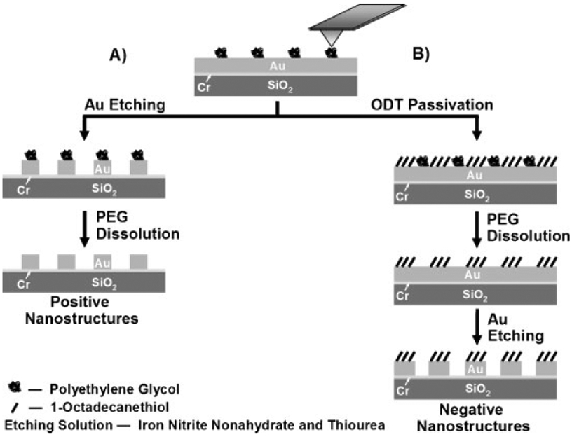
Polymer-based etch-resist methodology for generating positive and negative nanostructures.
In this work, DPN templates of PEG features are used as either a protective or sacrificial layer to generate raised or recessed structures on surfaces (Scheme 1). Derivatives of this polymer have been used as materials to minimize nonspecific adsorption of proteins and virus particles on surfaces such as Au and SiO2.[9,35-37] In a typical experiment, a cantilever array with 26 tips (A-26) was dipped into a 5mg mL−1 acetonitrile solution of PEG (MW 2000) for 10 s, then mounted onto an NSCRIPTOR and used to generate dots and lines on gold surfaces. Incubating the substrate in an aqueous etching solution containing 20mM thiourea and 30mM iron nitrate nonahydrate generates positive solid-state nanostructures (Scheme 1A). On the other hand, substrates that were subsequently passivated with 1mM ODT and washed with dichloromethane (to remove the PEG) before exposing to the same etching solution were used to produce negative nanoscale features (Scheme 1B). The resulting nanostructures were characterized by atomic force microscopy (AFM), scanning electron microscopy (SEM), and optical microscopy.
One of the attributes of DPN is the ability to tailor feature size by varying the scan rate of the tip array and tip–substrate contact time. There is typically a feature size dependence that correlates with the square root of the tip–substrate contact time.[16,38-40] The PEG exhibits a similar dependence when deposited on a 30-nm-thick Au film thermally evaporated on a SiO2 substrate. Scan rates of 0.05, 0.10, and 0.75 μm s−1 gave 175-, 105-, and 70-nm-wide line features, respectively (Figure 1A). On the other hand, dot features can be generated by holding the tip in contact with the substrate for set periods of time. Contact times of 0.5, 1, 2, 4, and 8 s at 80–90% humidity resulted in dot features with diameters of 100, 200, 300, 400, and 500 nm, respectively (Figure 1B).
Figure 1.
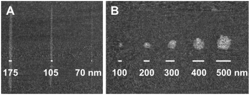
Lateral force microscopy (LFM) images of polyethylene glycol A) line and B) dot nanostructures generated using DPN.
After working out the protocol for patterning PEG, we evaluated the potential for using the PEG resist and wet chemical etching to generate positive solid-state features. As proof-of-concept, we used a 26-pen parallel array to generate twenty-six 15 × 20 PEG dot arrays on a gold thin-film surface. Each array consists of dots with deliberately generated 200-, 300-, 400-, and 500-nm-diameter features. The total time needed to generate the 26 identical PEG dot arrays was ≈1 h. The patterned substrate was subsequently etched using an aqueous solution of 20mM thiourea and 30mM iron nitrate nonahydrate to generate positive Au nanostructures with dot diameters of 205, 289, 400, and 517nm (±10 nm), respectively (Figure 2 A and B). Significantly, one can reduce the PEG feature size to the sub-100-nm scale simply by reducing the humidity to ≈70%. For example, contact times of 1, 2, 4, and 8 s resulted in PEG dot features with diameters of 80, 140, 178, and 234 nm, respectively (Figure 2C). We further show that a Au feature size down to 85nm thus far can be sequentially obtained using the above-generated PEG features as the etch resist (Figure 2D). There is remarkably good agreement between the sizes of the PEG resist features defined by DPN and the resulting solid-state raised nanostructures. AFM analysis of the solid-state features shows that on average they are 27 nm (±2 nm) high, which is equivalent to the thickness of the evaporated Au layer (≈30nm). These observations suggest that the PEG templates effectively protect the underlying gold regions, while the exposed gold areas were oxidized by the etching solution.
Figure 2.
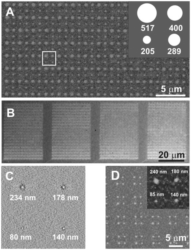
A) SEM and B) optical microscopy images of the generated positive Au nanostructures; C) contact-mode AFM image of PEG patterns used as etch resist to make the dot features in (D); D) tapping-mode AFM images of positive dot solid-state Au nanostructures generated from (C). One cell, which is designated by the white box in (A), is shown schematically in the inset of (A). The inset in (D) shows a zoomed-in AFM image of a generated Au dot array.
The DPN technique coupled with the novel PEG resist is quite versatile and allows one to generate very sophisticated structures, including complex shapes and patterns. As proof-of-concept, we used a digitized image of the Northwestern University logo and generated a PEG replica of it at 80-nm dot size resolution in dot matrix form (≈12000 features) on an Au thin film substrate in 50 min. This structure was etched as described above for 45 min, rinsed with CH2Cl2, and characterized by SEM (Figure 3A). Line arrays were similarly made and SEM and AFM post-etching analyses show the high uniformity and well-defined edges of the resulting features (Figure 3B and C). Each line, based upon AFM analysis (Figure 3C and D) is 150nm (±5 nm) wide, 6 μm long, and 27 nm (±2 nm) thick.
Figure 3.
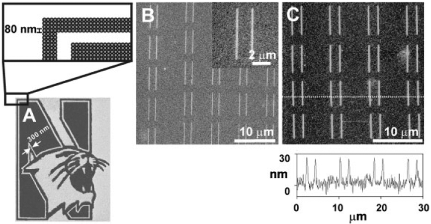
A) SEM image of a set of positive nanostructures in the form of the Northwestern University logo; the expanded area is a representation of the dot matrix map used to generate the structure; B) SEM image of positive line structures generated by DPN with the PEG resist and subsequent wet chemical etching; C) tapping-mode AFM image of the nanostructures shown in (B) and its corresponding height profile.
Interestingly, the PEG can not only be used to generate positive features but also negative ones. To generate negative features, we used the PEG as a sacrificial template (Scheme 1B). With this approach, we generate features made of PEG by DPN on a 60–70-nm-thick Au film, passivate the surrounding areas with ODT by immersing the substrate for 15 min in a 1mM ethanolic solution of ODT, and then rinse with CH2Cl2, which removes the PEG and residual physisorbed ODT. Subsequent etching results in the formation of negative features in the areas originally occupied by PEG. Using this approach, we have generated arrays of dot and line features and AFM and optical analysis of the resulting structures show that they are highly uniform (4% variation in line width, 7% variation in dot diameter; Figure 4). Height profiles show that the average depths of the generated nanostructures were similar to the thickness of the underlying gold layer (dots: ≈65 nm, lines: ≈58 nm). We intentionally used different Au film thicknesses (70nm for dot and 60nm for line; Figure 4A and B) to evaluate the versatility of the technique and how one can control the depth of negative features using this approach. As with the positive features, the use of the cantilever arrays shows how the process can be easily scaled (Figure 4C and D).
Figure 4.
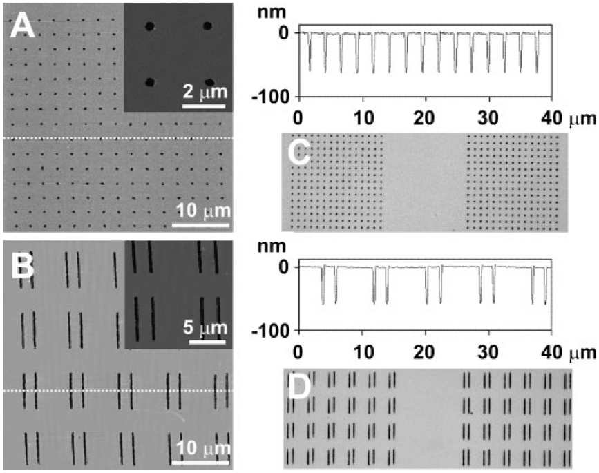
Tapping-mode AFM, height profile, and optical images of A,C) circular holes and B,D) line trenches generated using the negative feature polymer-based etching methodology. The insets in (A) and (B) show the zoomed-in AFM images of the negative nanostructures.
In summary, we have discovered that PEG can be used as a novel and extremely useful resist material for generating both positive and negative structures in the context of DPN. The PEG resist, when coupled with wet chemical etching, allows one to generate solid-state nanostructures in a manner that overcomes some of the limitations of the alkanethiol-based etching methods. Specifically, the polymer-based approach requires only a simple washing step to desorb materials from a substrate surface and, in principle, can be used with many types of underlying substrates (there is no requirement of chemisorption). Furthermore, the ability to generate a thick polymer layer and the elimination of the electrochemical desorption step associated with SAMs results in less pitting of the surface due to pinholes. Finally, the process works with parallel pen arrays, allowing one to pattern relatively large areas and it is likely extendable to other polymeric materials and perhaps other lithographic techniques.
Experimental Section
PEG templates were generated using DPN. A 26-tip array AFM probe was dip coated in a 5 mg mL−1 poly(ethylene glycol) acetonitrile solution for 10 s. The polymer-coated cantilever probes were then mounted on a NSCRIPTOR and PEG features were written on a thin layer of Au thermally evaporated on a SiO2 substrate with a 10-nm Cr adhesion layer. PEG templates that were first passivated with 1mM ODT for 15 min and rinsed with a dichloromethane solution, prior to incubation in an etching solution containing 20mM thiourea and 30mM iron nitrate nonahydrate, were used to generate negative nanostructures. Positive solid-state nanostructures were generated upon direct incubation of the PEG-patterned substrate in the same aqueous etching solution. The substrates were then rinsed with copious amounts of water to remove the PEG.
Supplementary Material
Acknowledgments
C. A. M. acknowledges DARPA, AFSOR, NSF, NSEC, and NCI (through the CCNE program) for support of the research. He is also grateful for a NIH Director’s Pioneer Award.
Footnotes
Supporting Information is available on the WWW under http://www.small-journal.com or from the author.
References
- [1].Ginger DS, Zhang H, Mirkin CA, Angew. Chem 2004, 116, 30–46; [DOI] [PubMed] [Google Scholar]; Angew. Chem. Int. Ed 2004, 43, 30–45. [Google Scholar]
- [2].Piner RD, Zhu J, Xu F, Hong SH, Mirkin CA, Science 1999, 283, 661–663. [DOI] [PubMed] [Google Scholar]
- [3].Liu X, Guo S, Mirkin CA, Angew. Chem 2003, 115, 4933–4937; [Google Scholar]; Angew. Chem. Int. Ed 2003, 42, 4785–4789. [DOI] [PubMed] [Google Scholar]
- [4].Jung H, Kulkarni R, Collier CP, J. Am. Chem. Soc 2003, 125, 12096–12097. [DOI] [PubMed] [Google Scholar]
- [5].Sheehan PE, Whitman LJ, King WP, Nelson BA, Appl. Phys. Lett 2004, 85, 1589–1591. [Google Scholar]
- [6].Lim J-H, Mirkin CA, Adv. Mater 2002, 14, 1474–1477. [Google Scholar]
- [7].Liu X, Zhang Y, Goswami DK, Okasinski JS, Salaita K, Bedzyk MJ, Mirkin CA, Science 2004, 307, 1763–1766. [DOI] [PubMed] [Google Scholar]
- [8].Noy A, Miller AE, Klare JE, Weeks BL, Woods BW, De Yoreo JJ, Nano Lett. 2002, 2, 109–112. [Google Scholar]
- [9].Lee K-B, Park S-J, Mirkin CA, Smith JC, Mrksich M, Science 2002, 295, 1702–1705. [DOI] [PubMed] [Google Scholar]
- [10].Jung H, Dalal CK, Kuntz S, Shah R, Collier CP, Nano Lett. 2004, 4, 2171–2177. [Google Scholar]
- [11].Li B, Zhang Y, Hu J, Li M, Ultramicroscopy 2005, 105, 312–315. [Google Scholar]
- [12].Lim J-H, Ginger DS, Lee K-B, Heo J, Nam J-M, Mirkin CA, Angew. Chem 2003, 115, 2411–2414; [DOI] [PubMed] [Google Scholar]; Angew. Chem. Int. Ed 2003, 42, 2309–2312. [DOI] [PubMed] [Google Scholar]
- [13].Su M, Liu X, Li S-Y, Dravid VP, Mirkin CA, J. Am. Chem. Soc 2002, 124, 1560–1561. [DOI] [PubMed] [Google Scholar]
- [14].Liu X, Fu L, Hong S, Dravid VP, Mirkin CA, Adv. Mater 2002, 14, 231–234. [Google Scholar]
- [15].John NS, Gundiah G, Thomas PJ, Kulkarni GU, Int. J. Nanosci 2005, 4, 921–934. [Google Scholar]
- [16].Huang L, Chang Y-H, Kakkassery JJ, Mirkin CA, J. Phys. Chem. B 2006, 110, 20756–20758. [DOI] [PMC free article] [PubMed] [Google Scholar]
- [17].Vega RA, Maspoch D, Salaita K, Mirkin CA, Angew. Chem 2005, 117, 6167–6169; [DOI] [PubMed] [Google Scholar]; Angew. Chem. Int. Ed 2005, 44, 6013–6015. [DOI] [PubMed] [Google Scholar]
- [18].Hong S, Mirkin CA, Science 2000, 288, 1808–1811. [DOI] [PubMed] [Google Scholar]
- [19].Hong S, Zhu J, Mirkin CA, Science 1999, 286, 523–525. [DOI] [PubMed] [Google Scholar]
- [20].Zhang H, Jin R, Mirkin CA, Nano Lett. 2004, 4, 1493–1495. [Google Scholar]
- [21].Ivanisevic A, Mirkin CA, J. Am. Chem. Soc 2001, 123, 7887–7889. [DOI] [PubMed] [Google Scholar]
- [22].Pena DJ, Raphael MP, Byers JM, Langmuir 2003, 19, 9028–9032. [Google Scholar]
- [23].Salaita K, Lee SW, Wang X, Huang L, Dellinger TM, Liu C, Mirkin CA, Small 2005, 1, 940–945. [DOI] [PubMed] [Google Scholar]
- [24].Salaita K, Wang Y, Fragala J, Vega RA, Liu C, Mirkin CA, Angew. Chem 2006, 118, 7378–7381; [DOI] [PubMed] [Google Scholar]; Angew. Chem. Int. Ed 2006, 45, 7220–7223. [DOI] [PubMed] [Google Scholar]
- [25].Zhang M, Bullen D, Chung SW, Hong S, Ryu KS, Fan ZF, Mirkin CA, Liu C, Nanotechnology 2002, 13, 212–217. [Google Scholar]
- [26].Love JC, Paul KE, Whitesides GM, Adv. Mater 2001, 13, 604–607. [Google Scholar]
- [27].Love JC, Estroff LA, Kriebel JK, Nuzzo RG, Whitesides GM, Chem. Rev 2005, 105, 1103–1169. [DOI] [PubMed] [Google Scholar]
- [28].Weinberger DA, Hong S, Mirkin CA, Wessels BW, Higgins TB, Adv. Mater 2000, 12, 1600–1603. [Google Scholar]
- [29].Xia Y, Zhao X-M, Kim E, Whitesides GM, Chem. Mater 1995, 7, 2323. [Google Scholar]
- [30].Zhang H, Chung S-W, Mirkin CA, Nano Lett. 2003, 3, 43–45. [Google Scholar]
- [31].Zhang H, Mirkin CA, Chem. Mater 2004, 16, 1480–1484. [Google Scholar]
- [32].Jang J-W, Maspoch D, Fujigaya T, Mirkin CA, Small 2007, 3, 600–605. [DOI] [PubMed] [Google Scholar]
- [33].Salaita KS, Lee SW, Ginger DS, Mirkin CA, Nano Lett. 2006, 6, 2493–2498. [DOI] [PubMed] [Google Scholar]
- [34].Zhang Y, Salaita K, Lim J-H, Lee K-B, Mirkin CA, Langmuir 2004, 20, 962–968. [DOI] [PubMed] [Google Scholar]
- [35].Lee K-B, Lim J-H, Mirkin CA, J. Am. Chem. Soc 2003, 125, 5588–5589. [DOI] [PubMed] [Google Scholar]
- [36].Prime KL, Whitesides GM, Science 1991, 252, 1164–1167. [DOI] [PubMed] [Google Scholar]
- [37].Lopez GP, Biebuyck HA, Harter R, Kumar A, Whitesides GM, J. Am. Chem. Soc 1993, 115, 10774–10781. [Google Scholar]
- [38].Manandhar P, Jang J, Schatz GC, Ratner MA, Hong S, Phys. Rev. Lett 2003, 90, 1155051–1155054. [DOI] [PubMed] [Google Scholar]
- [39].Cho N, Ryu S, Kim B, Schatz GC, Hong S, J. Chem. Phys 2006, 124, 0247141–0247145. [DOI] [PubMed] [Google Scholar]
- [40].Rozhok S, Piner R, Mirkin CA, J. Phys. Chem. B 2003, 107, 751–757. [Google Scholar]
Associated Data
This section collects any data citations, data availability statements, or supplementary materials included in this article.


