

Abstract
We report a low-cost, high-throughput scanning probe lithography method that uses a soft elastomeric tip array, rather than tips mounted on individual cantilevers, to deliver inks to a surface in a “direct write” manner. Polymer pen lithography merges the feature size control of dip-pen nanolithography with the large-area capability of contact printing. Because ink delivery is time and force dependent, features on the nanometer, micrometer, and macroscopic length scales can be formed with the same tip array. Arrays with as many as about 11 million pyramid-shaped pens can be brought into contact with substrates and readily leveled optically to ensure uniform pattern development.
Lithography is used in many areas of modern science and technology, including the production of integrated circuits, information storage devices, video screens, microelectromechanical systems (MEMS), miniaturized sensors, microfluidic devices, biochips, photonic bandgap structures, and diffractive optical elements (1-6). Generally, lithography can be divided into two categories on the basis of patterning strategy: parallel replication and serial writing. Parallel replication methods such as photolithography (7), contact printing (8-11), and nanoimprint lithography (12) are useful for high-throughput, large-area patterning. However, most of these methods can only duplicate patterns, which are predefined by serial writing approaches and thus cannot be used to arbitrarily generate different patterns (i.e., one photomask leads to one set of feature sizes for a given wavelength). In contrast, serial writing methods—including electron-beam lithography (EBL), ion beam lithography, and many scanning probe microscopy (SPM)–based methods (13-16)—can create patterns with high resolution and registration but are limited in throughput (17, 18). Indeed, only recently have researchers determined ways to use two-dimensional cantilever arrays for dip-pen nanolithography (DPN) to produce patterned structures made of molecule-based materials over areas as large as square centimeters (19, 20).
DPN uses an “ink”-coated atomic force microscope (AFM) tip to deliver soft or hard materials (e.g., molecular inks, nanoparticles, or sol gels) to a surface with high registration and sub-50-nm resolution in a “constructive” manner (3, 16, 21-23). When combined with high-density cantilever arrays, DPN is a versatile and powerful tool for constructing molecule-based patterns over relatively large areas with moderate throughput (1). The limitations of DPN are (i) the inability to easily and rapidly work across the micro- and nanometer-length scales in a single experiment (typically, either sharp tips are optimized to generate nanoscale features or blunt tips are used to generate microscale features) (24) and (ii) the need for fragile and costly two-dimensional cantilever arrays to achieve large-area patterning. Indeed, no simple strategy exists that allows one to rapidly pattern molecule-based features with sizes ranging from the nanometer to millimeter scale in a parallel, high-throughput, and direct-write manner. We report the development of polymer pen lithography (PPL), a low-cost, cantilever-free lithographic approach that, thus far, allows a digitized pattern to be printed at spot sizes ranging from 90 nm to hundreds of μm simply by changing the force and time over which the ink is delivered.
In contrast with DPN and other SPM-based lithographies, which typically use hard silicon–based cantilevers, PPL uses elastomeric tips without cantilevers [typically polydimethylsiloxane (PDMS)] (25, 26) to deliver ink. A typical polymer pen array (Fig. 1) contains thousands of pyramid-shaped tips that are made with a master prepared by conventional photolithography and subsequent wet chemical etching (fig. S1) (27). The pyramids are connected by a thin PDMS backing layer (50 to 100 μm thick) that is adhered to a glass support before curing. The glass support and thin backing layer significantly improve the uniformity of the polymer pen array over large areas, to date up to an entire 3-inch (76.2-mm) wafer surface (Fig. 1B and fig. S2) (27). When the sharp tips of the polymer pens are brought in contact with a substrate, ink is delivered at the points of contact (Fig. 1A). An important feature for ensuring uniform ink delivery over large areas is that the amount of light reflected from the tips increases greatly when the tips make contact with the substrate (movie S1) (27). Thus, the transparent elastomer polymer pen array allows us to determine visually when all of the pens are in contact with an underlying substrate. The otherwise daunting task of leveling the array can be tackled in an experimentally straightforward manner.
Fig. 1.
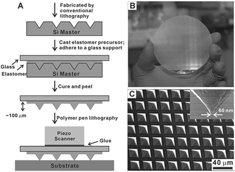
(A) A schematic illustration of the polymer pen lithography setup. (B) A photograph of an 11-million-pen array. (C) Scanning electron microscope image of the polymer pen array. The average tip radius of curvature is 70 ± 10 nm (inset).
We performed our PPL experiments with an Nscriptor system (NanoInk, Skokie, IL) equipped with a 90-μm closed loop scanner and commercial lithography software (DPNWrite, DPN System-2, NanoInk, Skokie, IL). Depending on intended use, the pitch of a pen array is deliberately set between 20 μm and 1 mm, corresponding to pen densities of 250,000/cm2 and 100/cm2, respectively. Larger pitch arrays are required to make large features (micrometer or millimeter scale) but also can be used to make nanometer-scale features. All of the pens are remarkably uniform in size and shape, with an average tip radius of 70 ± 10 nm (Fig. 1C). In principle, this value could be reduced substantially with higher-quality masters and stiffer elastomers. Finally, for many of the experiments we reported, we demonstrate capabilities with an array that contains either 15,000 or 28,000 pyramid-shaped pens, but we have made and demonstrated patterning capabilities with arrays with as many as ~11,000,000 pens (fig. S3) (27).
In a typical experiment, a polymer pen array (1 cm2 in size) was inked by immersing it in a saturated solution of 16-mercaptohexadecanoic acid (MHA) in ethanol for 5 min followed by rinsing with ethanol. The inked pen array was used for generating 1-μm diameter MHA dot patterns on a thermally evaporated polycrystalline gold substrate (25 nm Au with a 5 nm Ti adhesion layer coated on Si) by bringing it in contact with the gold surface for 0.1 s. This process was repeated 35 times to generate a 6 by 6 array of MHA dots (less than 10% deviation in feature diameter). The exposed gold on this MHA patterned substrate was subsequently etched (20 mM thiourea, 30 mM iron nitrate, 20 mM hydrochloric acid, and 2 mM octanol in water) to yield raised structures that are approximately 25 nm in height and easily imaged by optical microscopy (Fig. 2A).
Fig. 2.
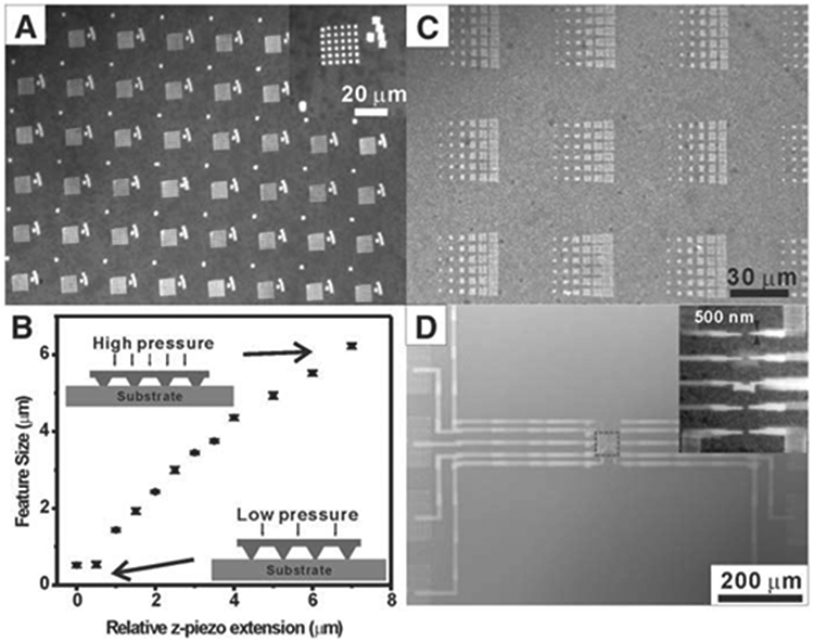
(A) Optical image of a 480-μm by 360-μm section of a one million gold dot array (6 by 6 within each block) on a silicon substrate (using a pen array with 28,000 pyramid-shaped tips). (B) MHA dot size as a function of relative z-piezo extension. The results were obtained using a polymer pen array with 15,000 pyramid-shaped tips at 25°C with a relative humidity of 40%. (C) Optical image of arrays of gold squares generated at different z-piezo extensions (using a pen array with 28,000 pyramid-shaped tips). (D) An optical microscope image of a multidimensional gold circuit fabricated by PPL. The inset shows a magnified SEM image of the circuit center.
A defining characteristic of PPL, in contrast with DPN and most contact printing strategies, which are typically viewed as force-independent (21), is that it exhibits both time- and force-dependent ink transport. As with DPN, features made by PPL exhibit a size that is linearly dependent on the square root of the tip-substrate contact time (fig. S4) (27-29). This property of PPL, which is a result of the diffusive characteristics of the ink and the small size of the delivery tips, allowed us to pattern submicrometer features with high precision and reproducibility (variation of feature size is less than 10% under the same experimental conditions).
The force dependence of PPL derives from the “soft” nature of the elastomer pyramid array. Indeed, the microscopic pyramidal tips can be made to deform with successively increasing amounts of applied force, which can be controlled by simply extending the piezo in the vertical direction (z-piezo). Although such deformation has been regarded as a major drawback in contact printing (it can result in “roof” collapse and limit feature size resolution), with PPL, the controlled deformation can be used as an adjustable variable, allowing control of the tip-substrate contact area and the resulting feature size. Within the force range allowed by z-piezo extension, one can observe a near linear relation between piezo extension and feature size at a fixed contact time of 1 s (Fig. 2B).
At the point of initial contact and a relative extension of 0.5 μm, the sizes of the MHA dots do not significantly differ and are both ~500 nm, indicating that the bulk of the polymer pen array compresses before the pyramid-shaped tips significantly deform. This observation is consistent with the known force-strain curves associated with PDMS (25). This type of buffering is fortuitous and essential for leveling because it provides extra tolerance in bringing all of the tips in contact with the surface without tip deformation and significantly changing the intended feature size. When the z-piezo extends 1 μm or more, the tips exhibit significant and controllable deformation (Fig. 2B).
Because of the force dependency of PPL, we do not have to rely on the time-consuming, meniscus-mediated ink diffusion process to generate large features. Indeed, we can generate either nanometer- or micrometer-sized features in only one printing cycle by simply adjusting the degree of tip deformation. As proof of concept, 6 by 6 gold square arrays, where each square in a row was written with one printing cycle at different tip-substrate forces but a constant 1-s tip-substrate contact time, were fabricated by PPL and subsequent wet chemical etching (Fig. 2C). The largest and smallest gold squares are 4 μm and 600 nm on edge, respectively. This experiment does not define the feature size range attainable in a PPL experiment but rather is a demonstration of the multiple scales accessible by PPL at a fixed tip-substrate contact time (1 s in this case).
Unlike conventional contact printing, PPL allows for the combinatorial patterning of molecule-based and solid-state features with dynamic control over feature size, spacing, and shape. As in conventional lithography of images, the polymer tips are used to form a dot pattern of the intended pattern or structure. As proof of concept, we used a polymer pen array with 100 pyramidal tips spaced 1 mm apart to generate 100 duplicates of an integrated gold circuit. The width of each electrode in the center of the circuit is 500 nm, whereas the width of each electrode lead going to these nanometer-scale electrodes is 10 μm, and the size of the external bonding pad is 100 by 100 μm2 (Fig. 2D). Because the Nscriptor provides only a 90 by 90 μm2 scanner, the circuits were divided into 35 80 by 80 μm2 subpatterns that were then stitched together by manually moving the stage motor after each subpattern was generated. This limitation could be addressed by programming the movement of the stage motor relative to the positions of the multiple subpatterns. To accommodate both resolution and throughput concerns, we used different relative z-piezo extensions at different positions of the circuit, where 0 (initial contact), 2, and 6 μm were used for the central electrodes, electrode leads, and bonding pads, respectively. As a result, writing a 100 by 100 μm2 area requires only 400 printing cycles (less than 0.5 s for each cycle), and the total time required to generate 100 duplicates of the circuit is ~2 hours. Re-inking of the pen array is not necessary because the PDMS behaves as a reservoir for the ink throughout the experiment (28, 29). This relatively high-throughput production of multiscale patterns would be difficult, if not impossible, to do by EBL or DPN.
The force dependence and maskless nature of PPL allow many structural variants to be created without the hurdle of designing a new master by a throughput-impeded serial process. In addition, PPL can be used with sub-100-nm resolution with the registration capabilities of a closed-loop scanner. For example, PPL was used to generate 15,000 replicas of the 2008 Beijing Olympic logo on gold with MHA as the ink and subsequent wet chemical etching (Fig. 3A). Each logo was generated using the multiscale capabilities of PPL from a 70 by 60 μm2 bitmap. The letters and numbers “Beijing 2008” were generated from ~20,000 90-nm dots (initial contact), whereas the picture and Olympic rings were made from ~4,000 600-nm dots at higher array-substrate contact forces (relative piezo extension = 1 μm). These structures were created by holding the pen array at each spot for 0.05 s and traveling between spots at a speed of 60 μm/s. A representative portion of the ~15,000 replicas (yield > 99%) generated across the 1-cm2 substrate shows their uniformity (Fig. 3B). The total time required to fabricate all of these structures was less than 40 min.
Fig. 3.
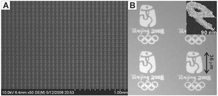
(A) SEM image of a representative region of ~15,000 miniaturized duplicates of the 2008 Beijing Olympic logo. (B) A zoom-in optical image of a representative replica. The inset shows a magnified SEM image of the letter “e.”
The time- and force-dependent ink transport properties of the polymer pen pyramid arrays provide a tunability to PPL that may allow other patterning capabilities to be developed. Because PPL is a direct-write technique, it is also ideal for fabricating arrays of structures made of soft matter, such as proteins (fig. S5) (27), making it potentially useful in the life sciences as well.
Supplementary Material
Footnotes
Supporting Online Material
References and Notes
- 1.Mirkin CA, ACS Nano 1, 79 (2007). [DOI] [PubMed] [Google Scholar]
- 2.Salaita K, Wang YH, Mirkin CA, Nat. Nanotechnol 2, 145 (2007). [DOI] [PubMed] [Google Scholar]
- 3.Ginger DS, Zhang H, Mirkin CA, Angew. Chem. Int. Ed 43, 30 (2004). [DOI] [PubMed] [Google Scholar]
- 4.Xia Y, Whitesides GM, Angew. Chem. Int. Ed 37, 550 (1998). [DOI] [PubMed] [Google Scholar]
- 5.Xia Y, Whitesides GM, Annu. Rev. Mater. Sci 28, 153 (1998). [Google Scholar]
- 6.Qi M et al. , Nature 429, 538 (2004). [DOI] [PubMed] [Google Scholar]
- 7.Ito T, Okazaki S, Nature 406, 1027 (2000). [DOI] [PubMed] [Google Scholar]
- 8.Loo YL, Willett RL, Baldwin KW, Rogers JA, J. Am. Chem. Soc 124, 7654 (2002). [DOI] [PubMed] [Google Scholar]
- 9.Zheng Z, Azzaroni O, Zhou F, Huck WTS, J. Am. Chem. Soc 128, 7730 (2006). [DOI] [PubMed] [Google Scholar]
- 10.Kumar A, Whitesides GM, Appl. Phys. Lett 63, 2002 (1993). [Google Scholar]
- 11.Yousaf MN, Houseman BT, Mrksich M, Proc. Natl. Acad. Sci. U.S.A 98, 5992 (2001). [DOI] [PMC free article] [PubMed] [Google Scholar]
- 12.Chou SY, Krauss PR, Renstrom PJ, Science 272, 85 (1996). [Google Scholar]
- 13.Xu S, Miller S, Laibinis PE, Liu GY, Langmuir 15, 7244 (1999). [Google Scholar]
- 14.Geissler M, Xia Y, Adv. Mater 16, 1249 (2004). [Google Scholar]
- 15.Gates BD et al. , Chem. Rev 105, 1171 (2005). [DOI] [PubMed] [Google Scholar]
- 16.Piner RD, Zhu J, Xu F, Hong S, Mirkin CA, Science 283, 661 (1999). [DOI] [PubMed] [Google Scholar]
- 17.Kramer S, Fuierer RR, Gorman CB, Chem. Rev 103, 4367 (2003). [DOI] [PubMed] [Google Scholar]
- 18.Maoz R, Cohen SR, Sagiv J, Adv. Mater 11, 55 (1999). [Google Scholar]
- 19.Lenhert S, Sun P, Wang Y, Fuchs H, Mirkin CA, Small 3, 71 (2007). [DOI] [PubMed] [Google Scholar]
- 20.Salaita K et al. , Angew. Chem. Int. Ed 45, 7220 (2006). [DOI] [PubMed] [Google Scholar]
- 21.Hong S, Mirkin CA, Science 288, 1808 (2000). [DOI] [PubMed] [Google Scholar]
- 22.Demers LM et al. , Science 296, 1836 (2002). [DOI] [PubMed] [Google Scholar]
- 23.Lee K-B, Park S-J, Mirkin CA, Smith JC, Mrksich M, Science 295, 1702 (2002). [DOI] [PubMed] [Google Scholar]
- 24.For instance, DPN fabrication of a 10-μm by 10-μm MHA feature on a gold substrate with a conventional Si3N4 cantilever (radius of curvature = 20 to 60 nm) takes ~30 min.
- 25.Schmid H, Michel B, Macromolecules 33, 3042 (2000). [Google Scholar]
- 26.Odom TW, Love JC, Wolfe DB, Paul KE, Whitesides GM, Langmuir 18, 5314 (2002). [Google Scholar]
- 27.Materials and methods are available as supporting material on Science Online.
- 28.Zhang H, Elghanian R, Amro NA, Disawal S, Eby R, Nano Lett. 4, 1649 (2004). [Google Scholar]
- 29.Wang X et al. , Langmuir 19, 8951 (2003). [Google Scholar]
- 30.C.A.M. acknowledges the U.S. Air Force Office of Scientific Research (AFOSR), the Defense Advanced Research Projects Agency (DARPA), and NSF (Nanoscale Science and Engineering Center program) for support of this research. C.A.M. is grateful for a NIH Director’s Pioneer Award and a National Security Science and Engineering Faculty Fellowship from the U.S. Department of Defense. L.R.G. acknowledges the NSF for a Graduate Research Fellowship.
Associated Data
This section collects any data citations, data availability statements, or supplementary materials included in this article.