

Dip-pen nanolithography (DPN) allows one to directly print a wide variety of biomaterials including DNA, phospholipids, and proteins on a surface with high registry and sub-50-nm resolution.[1–3] The recent development of massively parallel DPN has substantially increased the throughput of DPN through the use of 2D pen arrays consisting of as many as 55 000 atomic force microscopy (AFM) cantilevers per square centimeter.[4,5] Multiplexing, or the ability to simultaneously generate structures made of different materials, is the next step in developing a suite of DPN-based nanofabrication tools. Such capabilities will allow researchers to: 1) fabricate nanoarrays[6–10] with unprecedented chemical and biochemical complexity; 2) control materials assembly through the use of affinity templates,[11,12] such that each patterned feature controls the placement of different building blocks for fabricating higher-ordered architectures; and 3) develop an understanding of multivalent interactions between patterned surfaces and proteins, viruses, spores, and cells on a length scale that is biologically meaningful.[13–15] Methods for multiplexing in the context of a DPN experiment thus far have been limited owing to the challenges associated with addressing and inking each pen of an array with different molecules. The challenge extends beyond issues of cantilever addressability because a viable approach also requires uniform ink coating for different pens within an array and controlled transport rates for different ink molecules during a single experiment.
Hong et al. first demonstrated the direct DPN patterning of two different inks, 16-mercaptohexadecanoic acid (MHA) and 1-octadecanethiol (ODT), with high registry by using different tips in a serial process.[16] This approach provided little control over the diffusion rates of the two inks and the corresponding linewidths of the nanostructures generated in the experiment. Later, researchers developed microscopic inkwells that could be filled with various inks through integrated microfluidic channels. These inkwells were used to address the different pens in a 1D cantilever array for simultaneous DPN patterning of multiple inks from a single pen array.[17] This technique allows one to ink a linear pen array with up to eight different inks in a single step, depending on the number of available inkwells.[18] Although this approach works well for research applications where a few inks are being integrated in the context of a linear cantilever array comprising relatively few pens, the method is not directly scalable to 2D arrays consisting of thousands or even millions of pens. For instance, an inkwell chip containing 55 000 individually addressable ink wells in one square centimeter would require more than 0.5 m2 just to accommodate the area occupied by the ink reservoirs.
Herein, we describe a novel approach to inking pen arrays that addresses the multiplexed inking challenge in the context of DPN and related nanolithographies. Specifically, we independently address pens within 1D or 2D arrays with chemically distinct inks using an inkjet printer and introduce a new surface-modification strategy that directs the droplets of inks to the tips of the cantilevers. This method of delivery provides control over the inking process and transforms DPN into a general nanofabrication tool that uniquely combines high throughput, high resolution, and multiplexing capabilities (Scheme 1).
Scheme 1.
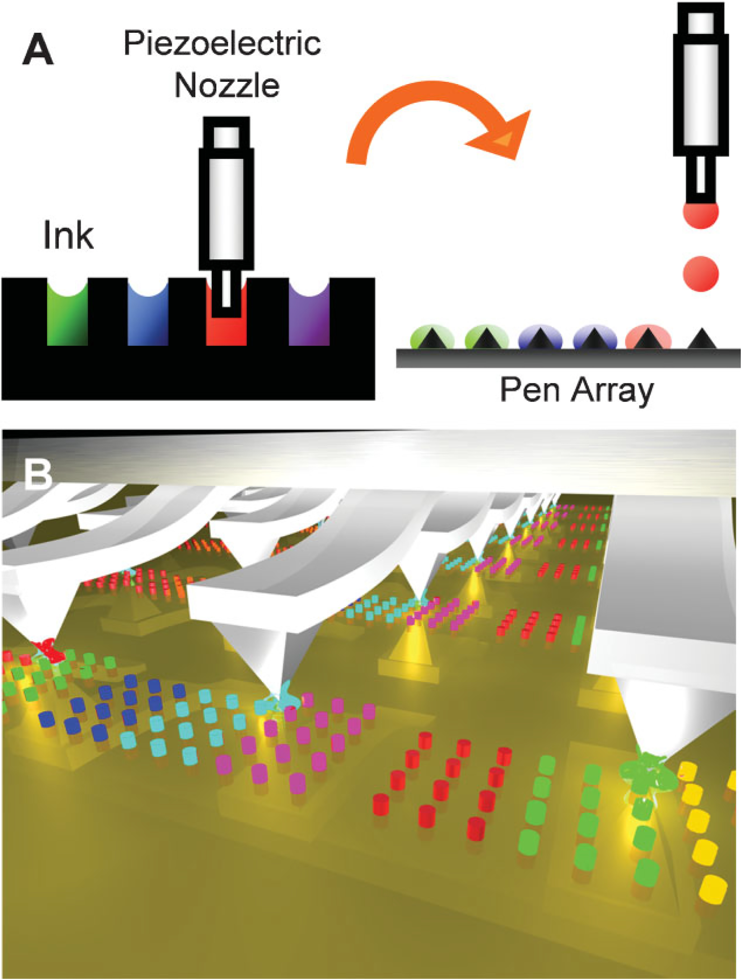
Schemes for A) addressable inking of pen arrays by inkjet printing and B) multiplexed dip-pen nanolithography.
We first demonstrate that inkjet printing allows one to independently address each pen within an array. Using a remote piezoelectric-controlled nozzle, the inkjet printer can directly deliver pico- to nanoliter volumes of ink to each pen. In air, the droplet diameters range from 40 to 100 μm, but increase to several hundred micrometers when they contact the substrate.[19–22] This inking protocol allows for the delivery of a large number of chemically distinct inks to each pen, or several pens, within a 1D or 2D pen array. To evaluate this approach, we initially studied the ability to address and coat every other pen in a 7-pen 1D array with an MHA/ethanol solution (10 mM, ~320 pL droplets), Figure 1A. This inkcoated pen array was then used in a DPN experiment to generate a 4 × 4 array of 1.5 mm diameter MHA features on a gold thin-film substrate. Subsequent etching of the exposed gold left raised features that could be easily characterized by optical microscopy, Figure 1B. Note that only the four inked cantilevers produced patterns. This experiment demonstrates that cantilevers spaced 150 μm apart can be addressed without cross-contamination.
Figure 1.
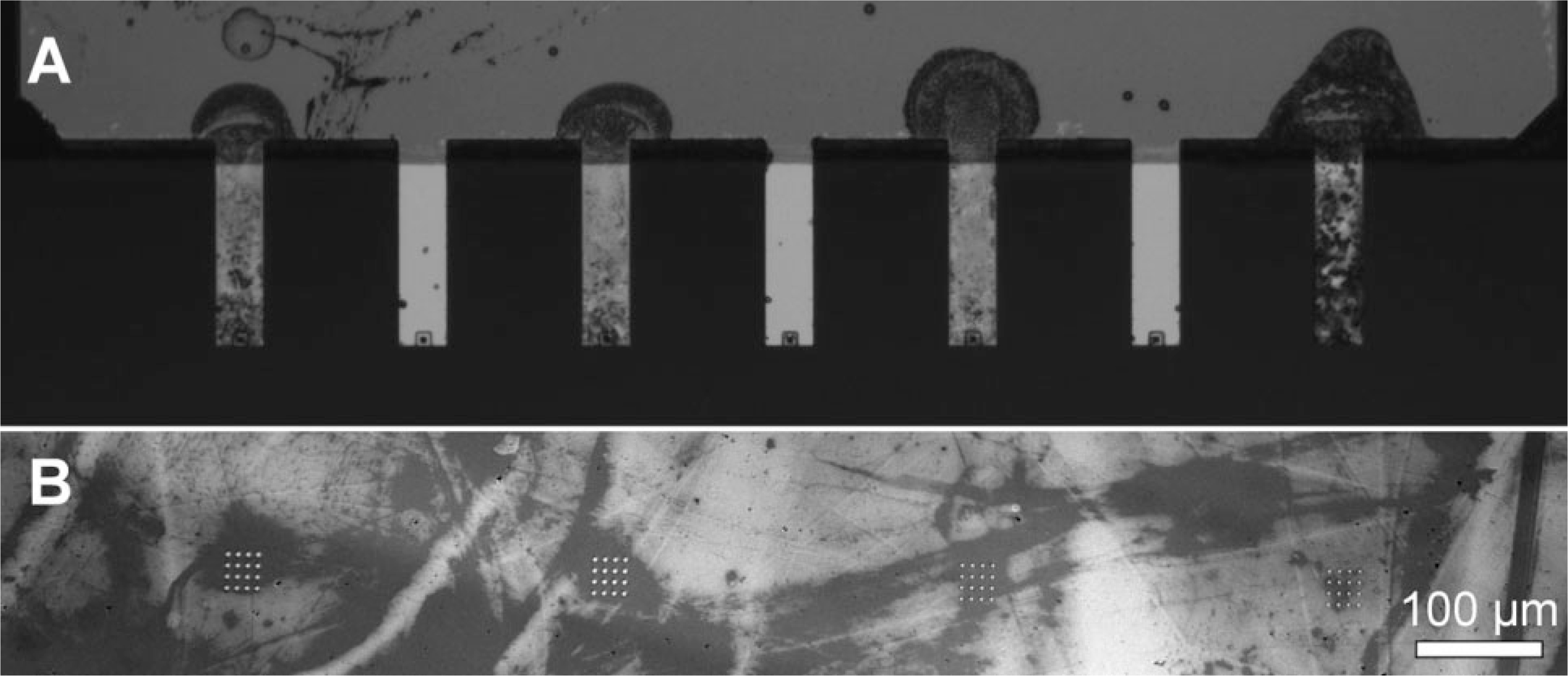
Addressable inking of a 1D pen array. A) Optical image of a 1D pen array with alternating pens inked with 1 drop of MHA-ethanol solution (10 mM, 320 pL) and B) the corresponding gold nanostructures patterned with the inked pen array.
Importantly, we found that delivering the same amount of MHA ink to different pens within an array using inkjet printing yields pattern features that are similar in size. Pattern sizes were measured by in situ lateral force microscopy (LFM) of the MHA patterns, by examining the aforementioned raised gold structures via optical microscopy, and also by AFM. The standard deviation of feature sizes generated by four different pens within the same array is (4.4 ± 1.4)% and increased only slightly among different pen arrays, to (4.8 ± 0.7)% (see Supporting Information, Figure S2). This size variation is remarkably small compared to dip-coated pen arrays, whose ink diffusion rates can vary by more than 10% from pen to pen (standard deviation) and are arbitrary from array to array (Supporting Information, Figure S3). The inked pen arrays have a shelf-life of at least one month and can generate high-quality features down to 100 nm with less than a 10% feature size variation.
These experiments confirmed that the large variation in diffusion rates associated with a pen array inked by dip-coating in a solution mainly arises from inhomogeneous ink distribution on the pens. Typically, the inking process involves pens soaking in an ink solution (e.g., a saturated solution of MHA in acetonitrile) for a few seconds, after which they are blow-dried with N2.[1,23–25] This process introduces variability due to inhomogeneous solvent drying, which can depend on the duration and angle of N2 blowing, as well as the manner of soaking. Because well-defined amounts of ink can be delivered with high spatial resolution to each pen, inkjet printing is a method that allows one to overcome the irreproducibility problems associated with inking from a solution.
To evaluate the prospects for multiplexing, we inked alternating cantilevers within a 7-pen array, each with different fluorophore-labeled phospholipids, by programming a single inkjet nozzle to go through cycles of aspiration, dispensing (inking), and cleaning for each of the four inks (Figure 2A). Each of the dye-labeled lipids was diluted (1 wt%) in a carrier lipid, 1,2-dioleoyl-sn-glycero-3-phosphocholine (DOPC). The use of DOPC as a carrier for multiplexed DPN is important for several reasons. First, it allows one to make the transport properties of different dye-labeled lipid inks uniform. Second, it is possible to incorporate up to ~25 wt% of certain functional lipids (such as biotinylated or nickel-chelating lipids) with DOPC. Third, being a major structural and functional component of biological membranes, phospholipids are well studied and compatible with many biological molecules.[18] The inked pen array was subsequently used to pattern four different inks in arrays of squares. Each square is 10 μm wide and made of 300 nm parallel line features. Significantly, the pen spacing is 150 μm, but using this technique and a mechanical stage, one can move pens in and out of the normal AFM field of view (90 μm × 90 μm), allowing one to construct structures made of different materials in one field of view (Figure 2B). This pattern demonstrates that inkjet printing can enable multiplexed DPN with multiple inks.[2,3,16]
Figure 2.
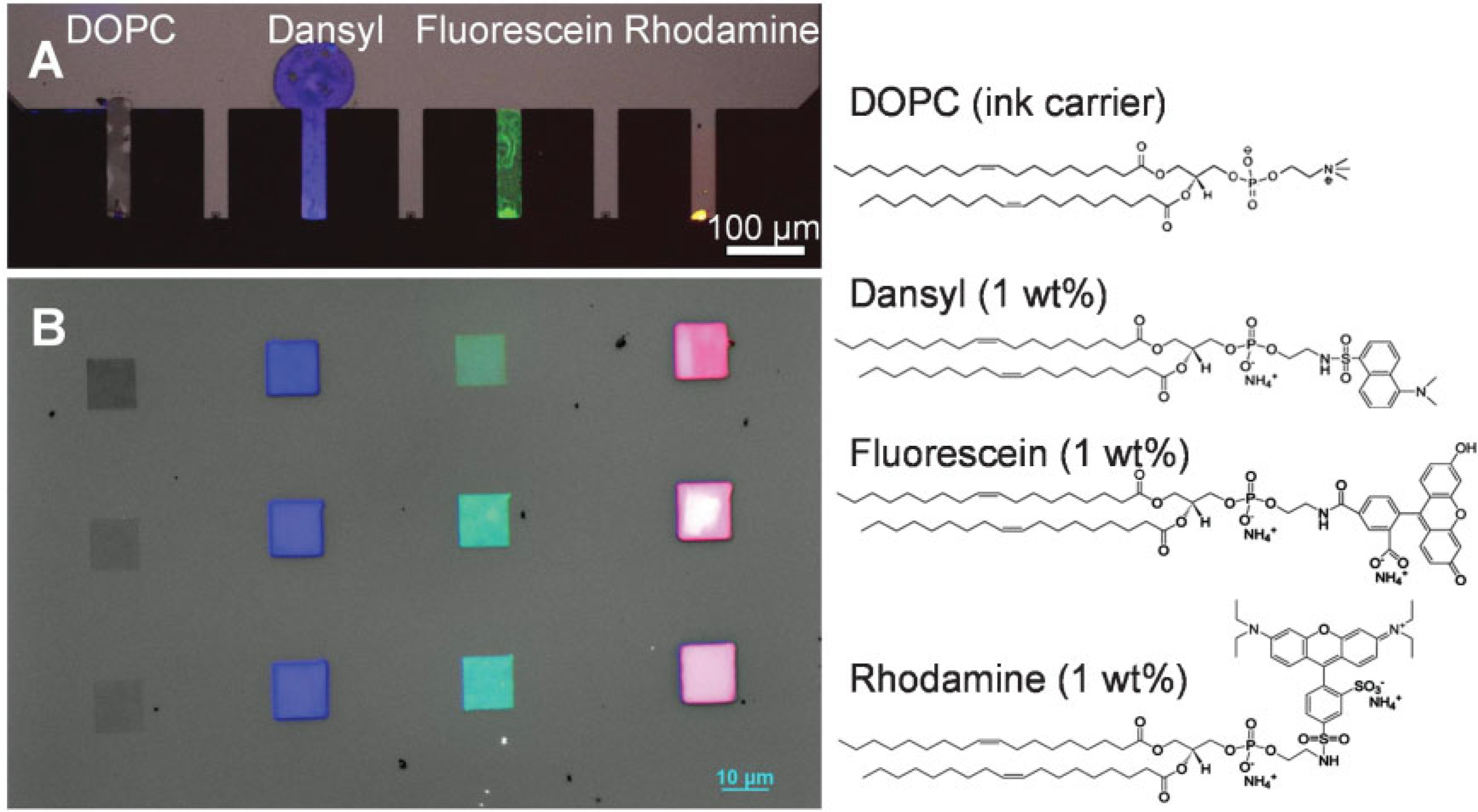
Fluorescent images showing individually addressable, multiplexed inking of a 1D pen array with phospholipids. A) A pen array inked with four different fluorophore-labeled phospholipids (structures shown on the right). B) Corresponding multiplexed patterns written on a glass slide.
Multiplexed inking of 2D arrays with multiple fluorophore-labeled phospholipids is also possible. In a proof-of-concept experiment, the gold-coated tips of a 55 000-pen 2D array[4,5] were functionalized with 1-mercaptoundecanol, and the remaining areas (silicon nitride and silicon/SiO2) were passivated with 1-octadecyltrichlorosilane (OTS). This chemical modification step is important as it overcomes the capillary-action-driven adhesion of inked cantilevers to the silicon/SiO2 support (Supporting Information, Figure S5). In one experiment, fluorophore-labeled phospholipids were printed on one quadrant of a 55 000-pen 2D array in the pattern of "NU" (Figure 3A and Supporting Information, Figure S4). The inked pen array was subsequently used for DPN patterning. Due to the 20 mm spacing between the adjacent pens of this 2D array, each inkjet droplet covered five to seven pens rather than one. Moreover, the inking was not perfectly uniform due to the spreading of droplets once they hit the substrate. Both of these issues can be addressed by increasing the pen-to-pen spacing in the array. Indeed, as proof of concept, single-pen addressability can be achieved by using a 2D pen array with 90mm 90mm pen-to-pen spacing (Figures 3B–D). It is important to note that the phospholipid ink droplets were better confined to the tips by functionalizing the gold-coated pens with a hydrophobic molecule, ODT; the droplet footprints decreased by ~50% compared to those on hydrophilic MHA-functionalized surfaces.
Figure 3.
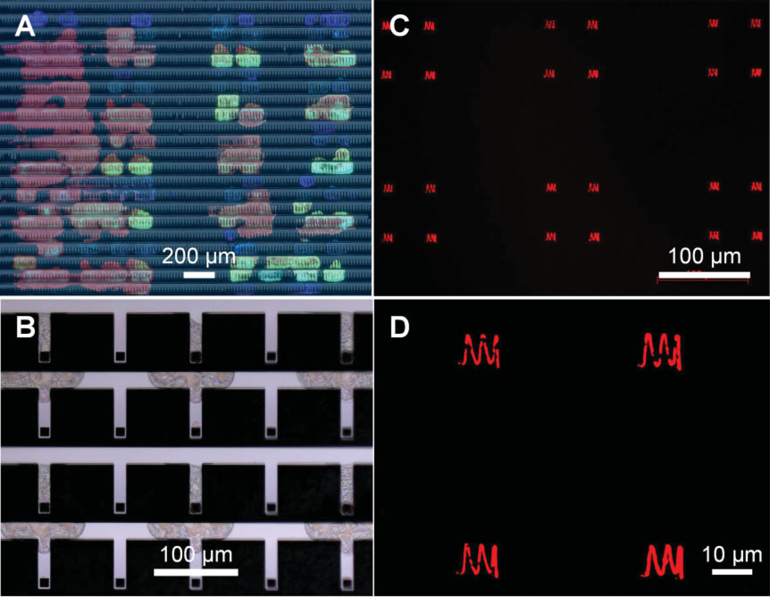
Addressable inking of 2D pen arrays with phospholipids. A) Four fluorophore-labeled phospholipids printed on a 2D pen array (90 μm × 20 μm spacing). B) Rhodamine-labeled phospholipid addressed to every other pen in a 2D array (90 μm × 90 μm spacing) and C,D) Corresponding 700 nm linewidth patterns written on a glass slide. Note that the cross-talk problem encountered in (A) is eliminated when the pen-to-pen spacing is increased to 90 μm × 90 μm.
Despite the addressability afforded by inkjet printing, the spatial resolution of inking is constrained by mechanical hysteresis, which limits registration of the inkjet printer with the pens in the array, the size of the nozzle (~85 μm diameter for the system used herein), occasional droplet formation inconsistencies, and the spreading of ink on the surface.[19–21] To overcome these problems, we have developed a self-correcting inking strategy that allows directed drying of the ink droplet based on chemical wetting and surface modification protocols[12,26,27] (Scheme 2). The basic idea is to functionalize the pen anisotropically so that the pyramidal tip is hydrophilic and the remaining area is hydrophobic. The anisotropic functionalization facilitates localization of an ink droplet on the hydrophilic tip due to differences in surface energy.
Scheme 2.
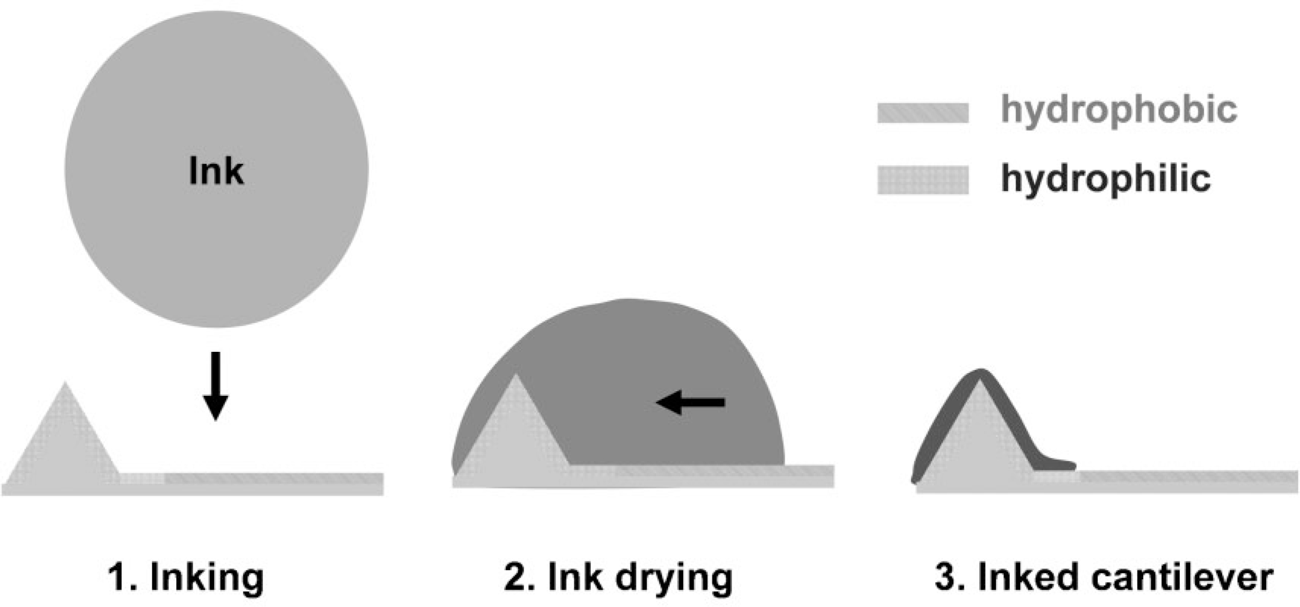
Scheme for self-correcting inking of an anisotropically functionalized pen. The pen is functionalized in such a way that the tip area is hydrophilic (MHA functionalization) and the remaining areas are hydrophobic (ODT functionalization). Ink molecules are preferentially driven to the hydrophilic area due to differences in surface energy.
As proof of concept, we selectively coated the tips of an array with a thin layer of gold using a cover slip as a shadow mask (Supporting Information, Figure S6). This approach allows one to locally functionalize the tip area with MHA through alkanethiol–gold chemistry[11] (Figure 4). Because the gold-deposition step can be integrated into the mold-and-transfer pen-microfabrication process,[4,28] this anisotropic functionalization strategy can be conveniently applied to both individual AFM cantilevers and pen arrays.[4] Using this approach and an inkjet printer to deliver 320 pL droplets onto individual pens within the array, such structures could be selectively addressed without contaminating neighboring pens (Figure 4A). The ink droplet was localized within the MHA-functionalized tip area, an area which is less than 2% of the total footprint area for an MHA/ethanol droplet drying on a MHA-functionalized gold substrate. This experiment, however, does not demonstrate the selective ink localization from the cantilever arm to the tip. To evaluate localization, a 0.2 μL droplet of 2 mM MHA/ethanol solution was deposited on the cantilever and tip areas of a 7-pen array (Figure 4B, five pens shown). Optical microscopy showed that as the droplet dries, the ink moves from the hydrophobic cantilever arm to the hydrophilic tip (see Supporting Information, movie). The liquid film breaks up at the hydrophobic–hydrophilic boundary, thereby confining the ink to the tip area (Figure 4B). A control experiment shows that the ink dries randomly on native SixNy cantilevers.
Figure 4.
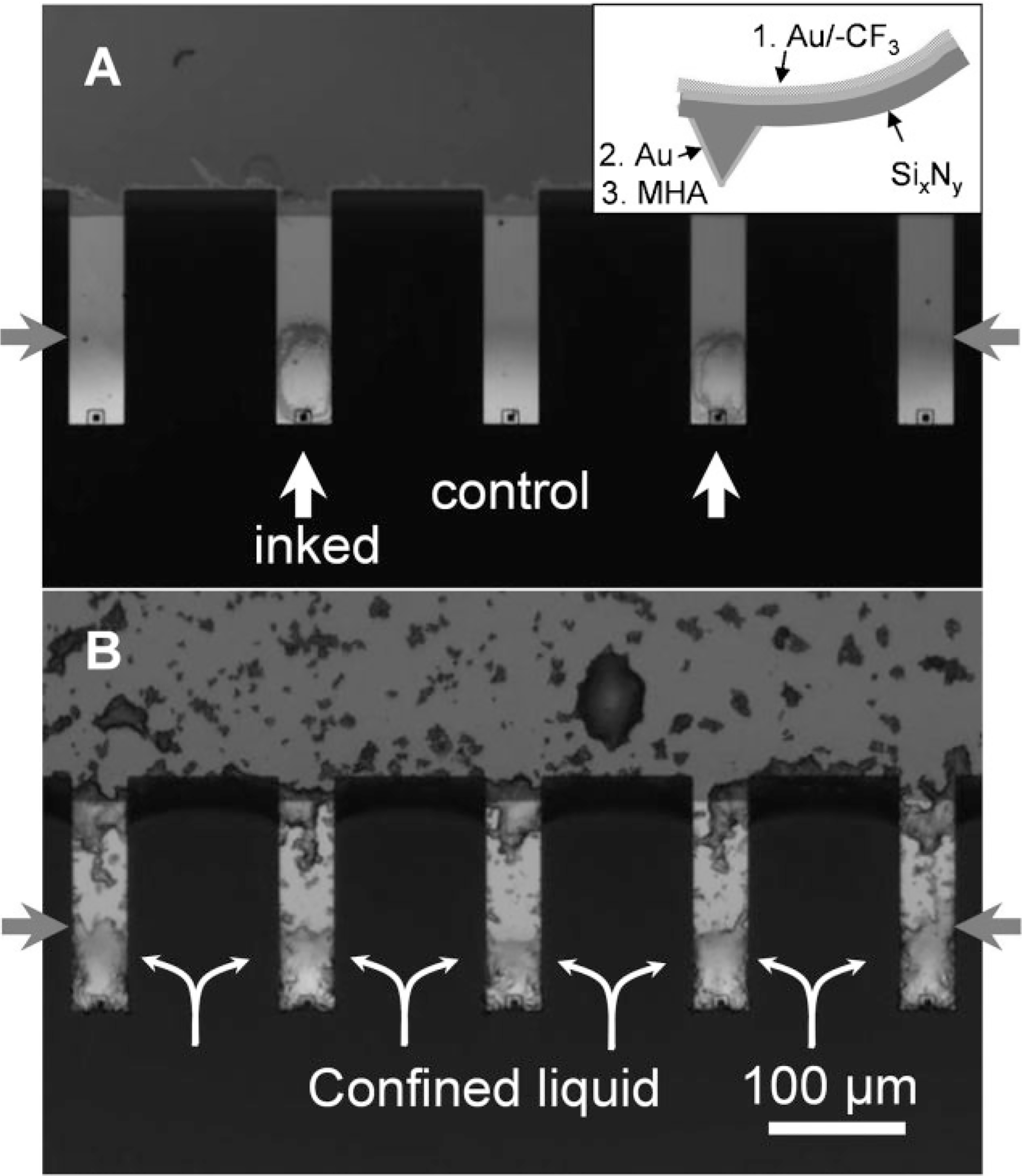
Self-correcting inking of anisotropically functionalized pens. A) Addressable inking of pens (white arrows) within a pen array by inkjet printing 3 drops of 10 mM MHA/ethanol solution (320 pL each) on each tip. The anisotropically functionalized areas (boundary marked by red arrows) dictate where the ink droplet dried. The inset shows the anisotropic functionalization of AFM probes, which consists of three steps: 1) coating the back side with a thin layer of 20 nm Au/5 nm Ti and functionalizing with 1H,1H,2H,2H-perfluorodecanethiol, 2) coating the front side of the tip area with gold (10 nm Au/4 nm Ti) using a glass cover slip as a shadow mask, and 3) selectively functionalizing the Au-coated front side of the tip with MHA. B) Optical microscopy image of anisotropically functionalized pens dip-coated with an MHA/ ethanol solution. Note that the ink is confined to the hydrophilic tip areas.
In another experiment, a gold-on-silicon substrate (25 nm gold/5 nm Ti/SiOx/Si) was modified with a monolayer of ODT, followed by a second deposition of gold on an area not covered by a glass cover slip. The second gold area was functionalized with MHA. This procedure creates a sharp boundary between the hydrophobic and hydrophilic portions of the substrate. An array of 10 mM MHA/ethanol ink droplets were deposited directly on and near the boundary, with varying droplet–boundary distances. For droplets that were within 230 μm of the boundary but on the ODT side, the ink droplets all moved to the MHA side of the substrate (Figure 5). Therefore, one does not have to perfectly address the tips of an array to achieve uniform tip inking because the ink on the cantilever arm will move to the tip.
Figure 5.
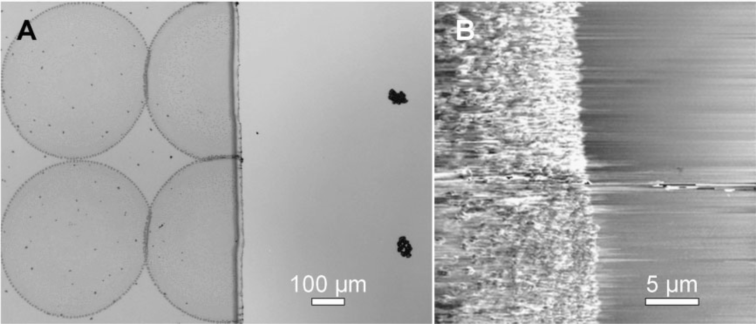
Footprints of inkjet droplets on and near a hydrophobic-hydrophilic boundary. A) A representative optical image showing the footprints of MHA ink droplets (320 pL, 10 mM in ethanol) printed near the MHA–ODT boundary. The footprint radii are (233.3 ± 6.2) μm for MHA (left) and (35.7 ± 3.7) mm for ODT (right). When a droplet hits the hydrophobic–hydrophilic boundary, the portion on the hydrophobic side is driven and localized to the MHA side (center). B) AFM image showing MHA was completely localized to the hydrophilic side.
Taken together, the inkjet and self-correcting inking strategy reported here provide a versatile and high-resolution method of addressing the multiplexed-inking challenge for DPN with 1D and 2D cantilever arrays. This work marks an important step towards the realization and practice of high-throughput, multiplexed, and consistent nanoscale patterning of soft matter. When one considers that we and others have shown the versatility of DPN for many types of inks,[2,3] it should be possible to extend the strategy to many classes of important molecules, including DNA, peptides, proteins, and other chemically and biologically relevant materials.
Experimental Section
Materials:
16-mercaptohexadecanoic acid (MHA, 90%), 1-octadecanethiol (ODT, 98%), and ethanol (200 proof, HPLC grade) were purchased from Sigma–Aldrich. Ti (99.7%) and Au (99.99%) wires were purchased from Alfa Aesar, Ward Hill, MA. All phospholipids were purchased from Avanti Polar Lipids, Inc. and include 1,2-dioleoyl-sn-glycero-3-phosphocholine (DOPC), 1,2-dioleoyl-sn-glycero-3-phosphoethanolamine-N-(lissamine Rhodamine B sulfonyl) ammonium salt (Rhodamine), 1,2-dioleoyl-sn-glycero-3-phosphoethanolamine-N-(5-dimethylamino-1-naphthalenesulfonyl) (Dansyl), and 1,2-dioleoyl-sn-glycero-3-phosphoethanolamine-N-(carboxyfluorescein) (Fluorescein).
Inkjet printing:
Inkjet printing was carried out using a drop-on-demand microdispensing system (Piezorray, Perkin Elmer, Inc., Waltham, MA) with an 85-μm piezoelectric-controlled nozzle that dispenses 320 pL droplets. The droplet formation was controlled by adjusting the voltage and pulse-width dispensing conditions (70 V, 40 μs), which could be monitored in real time using a charge-coupled device (CCD) camera. The system was enclosed in an environmental chamber, and the X–Y positional accuracy was 25 μm. Ink solutions included MHA in ethanol (0.5–10 mM), DOPC phospholipids in water (multilamellar vesicles at 10 g/L with 1 wt% fluorophore-labeled lipids), and saturated MHA–acetonitrile solutions.
Dip-pen nanolithography:
DPN experiments were performed with an NScriptor (NanoInk, Inc., Skokie, IL) or an AFM (CP-III, Veeco/Thermomicroscopes, Sunnyvale, CA) equipped with a 100-μm scanner and closed-loop scan control. All DPN patterning experiments were carried out under controlled environments (~40–75% relative humidity, 20–24 °C). Polycrystalline Au films were prepared by thermal evaporation of 5–10 nm of Ti on SiOx followed by 25 nm of Au at a rate of 1 Å/s and a base pressure of ≤5 × 10⁻⁶ Torr.
Supplementary Material
Acknowledgments
We thank NanoInk for the custom fabricated pen arrays. C.A.M. acknowledges the Air Force Office of Scientific Research, Defense Advanced Research Projects Agency, Army Research Office, National Science Foundation (NSF), and the National Institutes of Health through a Director’s Pioneer Award for support of this work. He is also grateful for an NSSEF Fellowship from the Department of Defense. L.R.G. thanks the NSF for a Graduate Research Fellowship. S.L. and H.F. thank the Deutsche Forschungsgemeinschaft (DFG) for financial support.
Footnotes
Supporting Information is available on the WWW under http://www.small-journal.com or from the author.
Contributor Information
Yuhuang Wang, Department of Chemistry, Department of Materials Science and Engineering, International Institute for Nanotechnology, Northwestern University, 2145 Sheridan Road, Evanston, Illinois 60208-3113 (USA).
Louise R. Giam, Department of Chemistry, Department of Materials Science and Engineering, International Institute for Nanotechnology, Northwestern University, 2145 Sheridan Road, Evanston, Illinois 60208-3113 (USA)
Matt Park, Department of Chemistry, Department of Materials Science and Engineering, International Institute for Nanotechnology, Northwestern University, 2145 Sheridan Road, Evanston, Illinois 60208-3113 (USA).
Steven Lenhert, Institut für NanoTechnologie, Forschungszentrum Karlsruhe GmbH 76021 Karlsruhe (Germany); Physikalisches Institut, Universität Münster 48149 Münster (Germany).
Harald Fuchs, Institut für NanoTechnologie, Forschungszentrum Karlsruhe GmbH 76021 Karlsruhe (Germany); Physikalisches Institut, Universität Münster 48149 Münster (Germany).
Chad A. Mirkin, Department of Chemistry, Department of Materials Science and Engineering, International Institute for Nanotechnology, Northwestern University, 2145 Sheridan Road, Evanston, Illinois 60208-3113 (USA).
References
- [1].Piner RD, Zhu J, Xu F, Hong SH, Mirkin CA, Science 1999, 283, 661. [DOI] [PubMed] [Google Scholar]
- [2].Ginger DS, Zhang H, Mirkin CA, Angew. Chem. Int. Ed. 2004, 43, 30. [DOI] [PubMed] [Google Scholar]
- [3].Salaita K, Wang Y, Mirkin CA, Nature Nanotechnol. 2007, 2, 145. [DOI] [PubMed] [Google Scholar]
- [4].Salaita K, Wang Y, Fragala J, Vega RA, Liu C, Mirkin CA, Angew. Chem. Int. Ed. 2006, 45, 7220. [DOI] [PubMed] [Google Scholar]
- [5].Lenhert S, Sun P, Wang Y, Fuchs H, Mirkin CA, Small 2007, 3, 71. [DOI] [PubMed] [Google Scholar]
- [6].Lee M, Kang D-K, Yang H-K, Park K-H, Choe SY, Kang C, Chang S-I, Han MH, Kang I-C, Proteomics 2006, 6, 1094. [DOI] [PubMed] [Google Scholar]
- [7].Lee K-B, Kim E-Y, Mirkin CA, Wolinsky SM, Nano Lett. 2004, 4, 1869. [Google Scholar]
- [8].Chen H, Li J, Methods in Molecular Biology 2007, 381, 411. [DOI] [PubMed] [Google Scholar]
- [9].Wingren C, Montelius L, Borrebaeck CAK, Protein Microarrays 2005, 339. [Google Scholar]
- [10].Mossman KD, Campi G, Groves JT, Dustin ML, Science 2005, 310, 1191. [DOI] [PubMed] [Google Scholar]
- [11].Love JC, Estroff LA, Kriebel JK, Nuzzo RG, Whitesides GM, Chem. Rev. 2005, 105, 1103. [DOI] [PubMed] [Google Scholar]
- [12].Wang Y, Maspoch D, Zou S, Schatz GC, Smalley RE, Mirkin CA, Proc. Nat. Acad. Sci. USA. 2006, 103, 2026. [DOI] [PMC free article] [PubMed] [Google Scholar]
- [13].Blanchette CD, Ratto TV, Longo ML, in Principles of Cellular Engineering: Micromechanics at the Biomolecular Interface, (Ed.: King MR), Elsevier, Burlington, MA: 2006, p. 195. [Google Scholar]
- [14].Stevens MM, George JH, Science 2005, 310, 1135. [DOI] [PubMed] [Google Scholar]
- [15].Christman KL, Enriquez-Rios VD, Maynard HD, Soft Matter 2006, 2, 928. [DOI] [PubMed] [Google Scholar]
- [16].Hong SH, Zhu J, Mirkin CA, Science 1999, 286, 523. [DOI] [PubMed] [Google Scholar]
- [17].Rosner B, Duenas T, Banerjee D, Shile R, Amro N, Rendlen J, Smart Mater. Struct. 2006, 15, S124. [Google Scholar]
- [18].Sekula S, Fuchs J, Weg-Remers S, Nagel P, Schuppler S, Fragala J, Theilacker N, Franzreb M, Wingren C, Ellmark P, Borrebaeck CAK, Mirkin CA, Fuchs H, Lenhert S, Small 2008, 4, 920–924. [DOI] [PubMed] [Google Scholar]
- [19].Calvert P, Chem. Mater. 2001, 13, 3299. [Google Scholar]
- [20].Sirringhaus H, Shimoda T, MRS Bull. 2003, 28, 802. [Google Scholar]
- [21].Zaugg FG, Wagner P, MRS Bull. 2003, 28, 837. [Google Scholar]
- [22].de Gans B-J, Kazancioglu E, Meyer W, Schubert US, Macromol. Rapid Commun. 2004, 25, 292. [Google Scholar]
- [23].Rozhok S, Piner R, Mirkin CA, J. Phys. Chem. B 2003, 107, 751. [Google Scholar]
- [24].Valiokas R, Vaitekonis S, Klenkar G, Trinkunas G, Liedberg B, Langmuir 2006, 22, 3456. [DOI] [PubMed] [Google Scholar]
- [25].Peterson EJ, Weeks BL, De Yoreo JJ, Schwartz PV, J. Phys. Chem. B 2004, 108, 15206. [Google Scholar]
- [26].Kargupta K, Sharma A, Phys. Rev. Lett. 2001, 86, 4536. [DOI] [PubMed] [Google Scholar]
- [27].Sehgal A, Ferreiro V, Douglas JF, Amis EJ, Karim A, Langmuir 2002, 18, 7041. [Google Scholar]
- [28].Zou J, Wang X, Bullen D, Ryu K, Liu C, Mirkin CA, J. Micromech. Microeng. 2004, 14, 204. [Google Scholar]
Associated Data
This section collects any data citations, data availability statements, or supplementary materials included in this article.