

Abstract
Two‐dimensional polymers (2DPs) are a class of atomically/molecularly thin crystalline organic 2D materials. They are intriguing candidates for the development of unprecedented organic–inorganic 2D van der Waals heterostructures (vdWHs) with exotic physicochemical properties. In this work, we demonstrate the on‐water surface synthesis of large‐area (cm2), monolayer 2D polyimide (2DPI) with 3.1‐nm lattice. Such 2DPI comprises metal‐free porphyrin and perylene units linked by imide bonds. We further achieve a scalable synthesis of 2DPI‐graphene (2DPI‐G) vdWHs via a face‐to‐face co‐assembly of graphene and 2DPI on the water surface. Remarkably, femtosecond transient absorption spectroscopy reveals an ultra‐fast interlayer charge transfer (ca. 60 fs) in the resultant 2DPI‐G vdWH upon protonation by acid, which is equivalent to that of the fastest reports among inorganic 2D vdWHs. Such large interlayer electronic coupling is ascribed to the interlayer cation–π interaction between 2DP and graphene.
Keywords: 2D polymers, graphene, interfacial synthesis, transient absorption spectroscopy, van der Waals heterostructure
We demonstrate a general but reliable on‐water synthesis and assembly strategy toward the preparation of 2D polyimide (2DPI)‐graphene (G) van der Waals heterostructures (vdWHs) on water surface. Remarkably, femtosecond transient absorption spectroscopy reveals an ultra‐fast interlayer charge transfer (ca. 60 fs) after protonation in the heterostructure, which is among the fastest reports of vdWHs.

Two‐dimensional (2D) van der Waals heterostructures (vdWHs) are generated by integration of 2D materials with dangling‐bond‐free surfaces through the weak interlayer vdW interaction along the vertical direction. [1] In recent years, synthetic 2D vdWHs have attracted increasing attentions due to the miscellaneous components and novel functions in phototransistors, [2] photodiodes, [3] memory devices [4] and tunneling devices. [5] Through surface reconstruction and proximity effects between the neighboring layers, the opto‐electrical properties of vdWHs can be tailored for tuning of carrier density, enhancement of electron‐hole separation, and accelerated charge transfer. [6] Furthermore, numerous exotic physical phenomena have emerged owing to the strong interlayer interactions such as moiré pattern in graphene/hexagonal boron nitride (G/h‐BN), [7] ultralong valley lifetime in WSe2/MoS2, [8] and strong spin–orbit coupling in graphene/WS2. [9] Despite versatile studies, 2D vdWHs reported so far are limited to inorganic 2D materials. It has remained largely unexplored to develop organic components for constructing organic–inorganic hybrid 2D vdWHs.
2D polymers (2DPs) have recently emerged as a new generation of atomically/molecularly thin organic 2D materials, which comprise repeated units linked via covalent bonds with long‐range order in two distinct directions. [10] Recent advances of on‐water surface synthesis strategies have paved the way to achieving single‐ to few‐layer crystalline 2DPs.[ 10a , 11 ] Owing to the homogenous, free‐standing, transferable and large‐area (up to cm2) characteristics,[ 10c , 11g ] the resultant 2DPs are attractive for the construction of 2D vdWHs.[ 11c , 11d , 11e ] Moreover, compared with inorganic 2D materials, 2DPs can be readily tailored to a much higher degree by using abundant building blocks and linkage chemistries. Thereby, 2DP‐based vdWHs are highly attractive owing to their tunable physicochemical properties and designable functions. Nevertheless, 2DP‐based vdWHs have remained rarely explored so far because of the challenge to synthesize structurally defined 2DP monolayers and to precisely assemble them with other 2D materials in a defined vdWH sequence. [12]
In this work, we demonstrated the preparation of 2D polyimide (2DPI)‐graphene (G) vdWH by the on‐water surface synthesis and assembly strategy. The 2DPI was firstly synthesized by polycondensation between 5,10,15,20‐tetrakis(4‐aminophenyl)porphyrin (M1) and perylene‐3,4,9,10‐tetracarboxylic dianhydride (M2), as shown in Figure 1 a. The achieved 2DPI is a large‐area (tens of cm2), free‐standing film with a sub‐nanometer thickness (0.8 nm). Subsequently, 2DPI‐G was built up by the assembly of 2DPI with electrochemically exfoliated graphene on the water surface and followed up by transferring to substrates with additional annealing. The unique structure of 2DPI‐G was proved by grazing incidence wide‐angle X‐ray scattering (GIWAXS), which presented a 3.14‐nm lattice for the 2DPI crystal and a 0.23‐nm lattice for graphene, thus demonstrating the co‐existence of both 2D materials in the vdWHs. Aberration‐corrected high‐resolution transmission electron microscopy (AC‐HRTEM) revealed hexagonal moiré fringes, indicating the face‐to‐face stacking between graphene and 2DPI. Remarkably, after the protonation of the porphyrin units in 2DPI (H‐2PI) by hydrochloric acid, the femtosecond transient absorption spectroscopy (fs‐TA) revealed that the H‐2DPI‐G displayed a strong acceleration of the relaxation dynamics related to an interfacial charge transfer from H‐2DPI to graphene. The interlayer charge transfer time of about 60 fs achieved in the H‐2DPI‐G heterostructure is comparable to that of the fastest reports among inorganic vdWHs, such as MoS2‐WS2 (50 fs) [13] and graphene‐WS2 (83 fs). [14]
Figure 1.

Reaction of the 2DPI by the LB method and illustration of 2DPI‐G vdWH. a) Synthesis of 2DPI on the water surface and face‐to‐face co‐assembly of graphene and 2DPI at the interface. b) Illustration of the 2DPI‐G fabrication on the water surface by LB method. There are six steps: Step 1: spread M1 onto the water surface; Step 2: well‐controlled compression induces the pre‐organization of M1; Step 3: Inject M2 into water subphase; Step 4: M2 is absorbed onto pre‐organized M1, triggering assembly and reaction; Step 5: disperse exfoliated graphene (EG) into the subphase; Step 6: 2DPI‐G formation via interfacial co‐assembly and subsequent annealing process.
The synthesis and fabrication of 2DPI‐G involve 6 steps, as illustrated in Figure 1 b. The procedure from Step 1 to Step 4 deals with the synthesis of 2DPI. In Step 1, a chloroform solution of M1 (0.1 mL, 1 mg mL−1) was spread onto the water surface. After 5 min evaporation of chloroform, the Delrin barriers were driven forward to compress M1 on the water surface at a rate of 1 mm min−1 (Step 2). When the surface pressure reached 10 mN m−1, M1 could be assembled as a monolayer with a mean molecular area (MMA) of 6 Å2, according to its surface pressure (SP)–mean molecular area (MMA) isotherm (Supporting Information, Figure S1). Then, M2 (20 mL, 1 mg mL−1, dissolved in 1 mg mL−1 LiOH aqueous solution, ca. 200 molar equivalents to M1) was gradually injected into the trough (Step 3). And the subphase was tuned to be alkaline (pH 11). M2 then slowly diffused to the air–water interface and got adsorbed onto the M1 monolayer and induced the 2D polymerization. After 30 h of reaction, we achieved a ca. 20 cm×7.5 cm thin film floating on the water surface (Step 4, Figure 1 a, Figure 2 a, Figure S2). Afterwards, the film was transferred onto a solid substrate and further annealed at 100 °C for 1 hour to complete the reaction of residual functional monomers and remove the water.
Figure 2.

Characterizations of 2DPI. a) Camera picture of the film on the water surface. b) Optical microscope image of the film with a rupture on a SiO2/Si substrate. Dash lines mark the edge of the films. c) AFM image on a SiO2/Si substrate. The height profile along the black line is inserted. d) SEM image on a copper grid with the hexagonal pores of 18 μm diameter (e) High‐resolution XPS spectrum of N 1 s region of M1 (bottom) and 2DPI (top). Nitrogen species of ‐NH2 (400.0 eV), imide (400.8 eV), and porphyrin core (including ‐N‐ at 398.4 eV and ‐NH‐ at ca. 400 eV) are marked in green, red, magenta, and violet, respectively. f) High‐resolution XPS spectrum at O1s region of M2 and 2DPI, the marked peaks at 533.18 eV (brown), and 531.58 eV (green) correspond to the character peaks of oxygen in C‐O‐C and C=O, respectively. g) ATR‐FTIR spectrum with marked reactive functional groups. h) Raman spectra of M1, M2, and 2DPI.
Figure 2 b presents the optical image of a homogenous 2DPI film with a straight rapture, showing the contrast between the bare substrate (SiO2/Si) and the film. The atomic force microscopy (AFM) measurement at the film edge revealed a thickness of 0.8 nm (Figure 2 c), suggesting the single‐layer feature. Due to AFM tip‐sample convolution effects, surface roughness of substrate (ca. 0.15 nm), and possible trapped solvents, the thickness measured by AFM is typically higher than the theoretical value for one monolayer (i.e., 0.43 nm).[ 11c , 15 ] Although the transfer procedure led to occasional film rupture, the ultrathin film could still cover almost the whole substrate and was mechanically stable to span over the hole of TEM grid as large as 18 μm (Figure 2 d). We performed X‐ray photoelectron spectroscopy (XPS) to investigate the elemental composition and chemical state of M1, M2, and 2DPI. We fit the high‐resolution N1s (Figure 2 e) and O1s (Figure 2 f) core level spectra with Gaussian‐Lorentzian sum peaks after the subtraction of a Shirley‐type baseline. Figure 2 f shows that the N ‐NH2 peak (at ca. 400 eV) is highly reduced after reaction; meanwhile, the imide (Nimide) peak emerged at 400.8 signaling the formation of the target imide bond. Additionally, Figure 2 f reveals the elimination of oxygen species of M2 (O C‐O‐C at 533.2 eV) after polymerization. Attenuated total reflection Fourier‐transform infrared spectroscopy (ATR‐FTIR) spectra indicated that the peak of the N‐H stretching of ‐NH2 (at 3364 cm−1) from M1 disappeared after polymerization (Figure 2 g). Meanwhile, the C=O vibration exhibited a blue shift from 1754 cm−1 for anhydride (M2) to 1695 cm−1 for imide (2DPI). In the Raman spectra of 2DPI (Figure 2 h), a characteristic peak of the imide C−N bond of 2DPI appeared at 1400 cm−1. Thereby, XPS, FTIR and Raman results clearly present the targeted imide bond formation and elimination of functional groups of the monomers, which strongly support the successful synthesis of 2DPI.
Following the synthesis of the 2DPI, Step 5 and Step 6 are concerned with the fabrication of the 2DPI‐G vdWHs. In Step 5, an aqueous suspension of high‐quality electrochemically exfoliated graphene [16] (EG has an average lateral size of ca. 2 μm and 80 % mono‐ to tri‐layer graphene; ca. 1 mg mL−1, 2 mL) was injected into the aqueous subphase (Figure 1 b). Graphene flakes then could attach to the bottom surface of the 2DP monolayer driven by the π‐π stacking interaction. To prepare the 2DPI‐G, we repeatedly transferred films to other substrates (Step 6 in Figure 1 b). As shown in Figure 3 a, the achieved vdWHs exhibited layered morphology via the repeated transfer method. The EG flakes are distributed in the 2DPI‐G without significant aggregation as can be seen in Figure 3 b. We then explored the crystal structure of 2DPI‐G. The chemical instability of ultrathin organic materials can always result in the collapse of their internal ordered structure and even decomposition at ambient condition, especially under electron radiation. [11c] To solve this problem, grazing incidence wide‐angle X‐ray scattering (GIWAXS) was utilized to characterize the pristine crystal structures of 2DPI‐G. Moreover, the 2DPI film is encapsulated by graphene in the case of 2DPI‐G, which prevents radiation damage during the measurement. [11c] The 2D‐GIWAXS pattern in Figure 3 c shows diffraction rings at 0.20 Å−1, 1.48 Å−1, 2.21 Å−1 and 2.53 Å−1, which correspond to d‐space values of 31.4 Å, 4.24 Å, 2.84 Å and 2.48 Å, respectively. The ring at 31.4 Å can be attributed to the 100 or 010 Bragg peaks of 2DPI, consistent with the calculated results (Figure 3 e). The peak at 4.24 Å corresponds to the layer distance of few‐layer stacking EG. [17] The peak at 2.84 Å are mainly distributed along the out‐of‐plane direction, which could originate from the higher‐order Bragg diffraction of interlayer structure. The peak at 2.48 Å is assigned to the lattice constant of graphene (a=b=2.46 Å). [18] Moreover, this ring mainly lies in the in‐plane direction, suggesting that the EG flakes prefer a face‐on orientation in the vdWHs.
Figure 3.
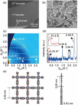
Morphology and structural characterization of 2DPI‐G. a) SEM image and b) low‐magnification TEM images of 2DPI‐G heterostructure after twice deposition. The edges of the graphene flakes were marked by dashed lines. c) 2D‐GIWAXS pattern of 2DPI‐G. d) The profile of integrated intensity of GIWAXS pattern with a zoom‐in view of low Qxy region. e) The model from DFT calculation, showing both top view and side view.
The 2DPI‐G heterostructures are visualized with aberration‐corrected high‐resolution transmission electron microscopy (AC‐HRTEM). As shown in Figure 4 a, one can observe moiré patterns in the 2DPI‐G, which is caused by the misoriented stacking of the graphene layers as a typical phenomenon in vdWHs. [19] Figure 4 b presents a highly ordered in‐plane structure in the selected area as marked in Figure 4 a. Its FFT pattern reveals that the superlattice structure has hexagonal moiré fringes with periodicity of ca. 9.39 and ca. 5.62 nm, demonstrating the face‐on orientation of 2DPI‐G. However, unlike GIWAXS investigation, we did not observe the 3.0 nm periodicity in the TEM image, which is mostly due to the extreme sensitivity of 2DPI monolayer toward electron irradiation damage. Figure 4 c shows a zoom‐in image of the selected part of Figure 4 b, which manifests the superlattice structures. The graphene lattice with d space of 0.24 nm was presented with higher magnification at the atomic resolution (showing 0.22 nm in Figure 4 d). It should be noted that different superlattices can be observed, which are attributed to the random rotation of EG during the co‐assembly with 2DPI (Figure S3).
Figure 4.

TEM images of the 2DPI‐G vdWHs. a) Low‐magnification TEM image. b) TEM image of the marked area in (a) clearly showing the moiré patterns. c) The zoom‐in image of the marked area in (b) shows the superlattice at higher magnification. d) Zoom‐in image of the marked area in (c) showing the crystalline lattice of EG.
Ultraviolet‐visible (UV/Vis) absorption spectroscopy and transient absorption (TA) are employed to study the intrinsic optical properties of 2DPI and 2DPI‐G and the interlayer coupling phenomenon within 2DPI‐G. Figure 5 a shows that porphyrin units are dominant in the absorption spectrum of 2DPI with the characteristic Soret band at ca. 440 nm and Q bands at 548 and 665 nm. Figure 5 b exhibits the increase of absorbance after the repeated horizontal transfer of 2DPI onto quartz substrates. The light absorption strongly depends on the layer thickness, which presents a linear correlation (Figure 5 c) between the number of layers and the absorbance value of the S band, following the Beer–Lambert law. This result suggests that multilayer structures of 2DPI are homogenous over the thin films.
Figure 5.

Optical properties of 2DPI‐G heterostructure. a) UV/Vis absorption of monomers and 2DPI. b) Spectra of 2DPI with the different number of layers from 1 layer to 6 layers. c) The absorbance intensity of Soret bands versus layer numbers, showing a linear relationship. d) UV/Vis absorption spectra of 2DPI‐G (black) and H‐2DPI‐G (red). The spectrum of 2DPI (blue dash) is also added as the reference. e) Dynamics of transient absorption in multi‐layer graphene (blue dots), protonated 2DPI (red dots) and protonated 2DPI‐G (green dots) measured using a degenerate pump‐probe spectroscopy setup with fs pulses at 470 nm. The inset shows the sub‐ps dynamics immediately after the photoexcitation.
The relaxation dynamics of charge carriers in 2DPI‐G was characterized by the TA spectroscopy. However, we only obtained the signal of graphene in 2DPI‐G samples (Figure S4), because relaxation in graphene dominates the decay process which diminishes the signal of 2DPI. This result also indicates that the interlayer charge transfer is not significant due to the weak electronic interaction between pristine 2DPI and graphene. To overcome this obstacle, we protonated 2DPI‐G with HCl (37 %wt), which is denoted as H‐2DPI‐G. Compared with 2DPI‐G and 2DPI, the S band of H‐2DPI‐G significantly broadened (Figure 5 d) due to a shoulder peak formation, which could be further divided into a narrow absorption peak at 438 nm and a broad absorption peak at 481 nm (Figure S5). The Q bands (400 nm to 600 nm) were red‐shifted and merged into a single broad band peaked at 709 nm. The significant red shift of absorption band is related to the cation‐π interaction between graphene and porphyrin structures in the vdWH, which can enhance the interlayer interaction in H‐2DPI‐G. [20] Moreover, compared with 2DPI‐G before protonation, the redshift also indicates an intrinsically smaller band gap that is positive for charge transfer from H‐2DPI to graphene. [12c]
Figure 5 e presents a noticeable acceleration of the relaxation dynamics of H‐2DPI‐G with near‐resonant excitation at 470 nm. Both fast and slow decay processes of H‐2DPI‐G are influenced by the charge transfer from H‐2DPI to graphene. The most remarkable effect is the emergence of the pronounced fast relaxation process caused by the proximity of the graphene layer. By comparing the UV/Vis absorption around 470 nm (see Figure 5 d), the fast decay in H‐2DPI‐G is attributed to the relaxation of the lower energy level. Fitting with a bi‐exponential decay function gives the relaxation time constants of the fast and slow decays in H‐2DPI‐G that are equal to 61.5±6.5 fs and 1700±100 fs, respectively (Table S1, see detailed discussion in Supporting Information). The timescale of ca. 60 fs of the dominating relaxation defines the speed of the interlayer charge transfer in H‐2DPI‐G. Similar timescales have been reported for ultra‐fast charge transfer in inorganic vdWHs, i.e., transition‐metal dichalcogenide/graphene heterostructures.[ 13 , 14 ]
In summary, we demonstrated the novel on‐water surface synthesis of 2DPI and its assembly with graphene for the construction of unprecedented 2DPI‐based vdWHs. Guided by the strong interlayer cation‐π interaction between protonated H‐2DPI and graphene, the resultant H‐2DPI‐G exhibited remarkable ultra‐fast charge transfer within 60 fs. The on‐water surface synthesis approach holds promise as a general method for the preparation of organic‐inorganic vdWHs. The structures of 2DPs can be further adjusted for engineering their band gaps and enhancing the charge transfer. A critical aspect of the future work will be the study of organic‐inorganic interlayer coupling that can lead to unique quantum phenomena.
Conflict of interest
The authors declare no conflict of interest.
Supporting information
As a service to our authors and readers, this journal provides supporting information supplied by the authors. Such materials are peer reviewed and may be re‐organized for online delivery, but are not copy‐edited or typeset. Technical support issues arising from supporting information (other than missing files) should be addressed to the authors.
Supplementary
Acknowledgements
We acknowledge financial support from EU Graphene Flagship (Core3, No. 881603), ERC Grants on T2DCP and FC2DMOF (No. 852909) and DFG projects (SFB‐1415, No. 417590517; SPP 2244, 2DMP) as well as the German Science Council, Centre of Advancing Electronics Dresden, EXC1056 (Center for Advancing Electronics Dresden) and OR 349/1. We thank Prof. Xiaodong Zhuang (Shanghai Jiao Tong University) and Prof. Zhikun Zheng (Sun Yat‐sen University) for fruitful discussions. We acknowledge Dresden Center for Nanoanalysis (DCN) for scanning electron microscopy and Dr. Petr Formanek (Leibniz Institute for Polymer Research, IPF, Dresden) for the use of facilities. We acknowledge Diamond Light Source for time on Beamline I07 under Proposal SI25070. Open access funding enabled and organized by Projekt DEAL.
K. Liu, J. Li, H. Qi, M. Hambsch, J. Rawle, A. R. Vázquez, A. S. Nia, A. Pashkin, H. Schneider, M. Polozij, T. Heine, M. Helm, S. C. B. Mannsfeld, U. Kaiser, R. Dong, X. Feng, Angew. Chem. Int. Ed. 2021, 60, 13859.
Contributor Information
Dr. Renhao Dong, Email: renhao.dong@tu-dresden.de.
Prof. Dr. Xinliang Feng, Email: xinliang.feng@tu-dresden.de.
References
- 1.
- 1a. Novoselov K. S., Mishchenko A., Carvalho A., Castro Neto A. H., Science 2016, 353, aac9439; [DOI] [PubMed] [Google Scholar]
- 1b. Geim A. K., Grigorieva I. V., Nature 2013, 499, 419–425. [DOI] [PubMed] [Google Scholar]
- 2. Xu H., Wu J., Feng Q., Mao N., Wang C., Zhang J., Small 2014, 10, 2300–2306. [DOI] [PubMed] [Google Scholar]
- 3. Jariwala D., Sangwan V. K., Wu C. C., Prabhumirashi P. L., Geier M. L., Marks T. J., Lauhon L. J., Hersam M. C., Proc. Natl. Acad. Sci. USA 2013, 110, 18076–18080. [DOI] [PMC free article] [PubMed] [Google Scholar]
- 4. Bertolazzi S., Krasnozhon D., Kis A., ACS Nano 2013, 7, 3246–3252. [DOI] [PubMed] [Google Scholar]
- 5. Georgiou T., Jalil R., Belle B. D., Britnell L., Gorbachev R. V., Morozov S. V., Kim Y.-J., Gholinia A., Haigh S. J., Makarovsky O., Eaves L., Ponomarenko L. A., Geim A. K., Novoselov K. S., Mishchenko A., Nat. Nanotechnol. 2013, 8, 100–103. [DOI] [PubMed] [Google Scholar]
- 6.
- 6a. Dereka B., Rosspeintner A., Krzeszewski M., Gryko D. T., Vauthey E., Angew. Chem. Int. Ed. 2016, 55, 15624–15628; [DOI] [PubMed] [Google Scholar]; Angew. Chem. 2016, 128, 15853–15857; [Google Scholar]
- 6b. Zheng Q., Saidi W. A., Xie Y., Lan Z., Prezhdo O. V., Petek H., Zhao J., Nano Lett. 2017, 17, 6435–6442; [DOI] [PubMed] [Google Scholar]
- 6c. Jakowetz A. C., Böhm M. L., Zhang J., Sadhanala A., Huettner S., Bakulin A. A., Rao A., Friend R. H., J. Am. Chem. Soc. 2016, 138, 11672–11679; [DOI] [PubMed] [Google Scholar]
- 6d. Petoukhoff C. E., Krishna M. B. M., Voiry D., Bozkurt I., Deckoff-Jones S., Chhowalla M., O'Carroll D. M., Dani K. M., ACS Nano 2016, 10, 9899–9908; [DOI] [PubMed] [Google Scholar]
- 6e. Tan H., Xu W., Sheng Y., Lau C. S., Fan Y., Chen Q., Tweedie M., Wang X., Zhou Y., Warner J. H., Adv. Mater. 2017, 29, 1702917. [DOI] [PubMed] [Google Scholar]
- 7. Yankowitz M., Xue J., Cormode D., Sanchez-Yamagishi J. D., Watanabe K., Taniguchi T., Jarillo-Herrero P., Jacquod P., Leroy B. J., Nat. Phys. 2012, 8, 382–386. [Google Scholar]
- 8. Kim J., Jin C., Chen B., Cai H., Zhao T., Lee P., Kahn S., Watanabe K., Taniguchi T., Tongay S., Crommie M. F., Wang F., Sci. Adv. 2017, 3, e1700518. [DOI] [PMC free article] [PubMed] [Google Scholar]
- 9. Wang Z., Ki D. K., Chen H., Berger H., Macdonald A. H., Morpurgo A. F., Nat. Commun. 2015, 6, 8339. [DOI] [PMC free article] [PubMed] [Google Scholar]
- 10.
- 10a. Sahabudeen H., Dong R., Feng X., Chimia 2019, 73, 480–486; [DOI] [PubMed] [Google Scholar]
- 10b. Qi H., Sahabudeen H., Liang B., Položij M., Addicoat M. A., Gorelik T. E., Hambsch M., Mundszinger M., Park S., Lotsch B. V., Mannsfeld S. C. B., Zheng Z., Dong R., Heine T., Feng X., Kaiser U., Sci. Adv. 2020, 6, eabb5976; [DOI] [PMC free article] [PubMed] [Google Scholar]
- 10c. Dong R., Zhang T., Feng X., Chem. Rev. 2018, 118, 6189–6235; [DOI] [PubMed] [Google Scholar]
- 10d. Sakamoto J., van Heijst J., Lukin O., Schluter A. D., Angew. Chem. Int. Ed. 2009, 48, 1030–1069; [DOI] [PubMed] [Google Scholar]; Angew. Chem. 2009, 121, 1048–1089. [Google Scholar]
- 11.
- 11a. Liu K., Wang L., Dong R., J. Mater. Chem. C 2020, 8, 10696–10718; [Google Scholar]
- 11b. Liu K., Qi H., Dong R., Shivhare R., Addicoat M., Zhang T., Sahabudeen H., Heine T., Mannsfeld S., Kaiser U., Zheng Z., Feng X., Nat. Chem. 2019, 11, 994; [DOI] [PubMed] [Google Scholar]
- 11c. Sahabudeen H., Qi H., Glatz B. A., Tranca D., Dong R., Hou Y., Zhang T., Kuttner C., Lehnert T., Seifert G., Kaiser U., Fery A., Zheng Z., Feng X., Nat. Commun. 2016, 7, 13461; [DOI] [PMC free article] [PubMed] [Google Scholar]
- 11d. Dai W., Shao F., Szczerbinski J., McCaffrey R., Zenobi R., Jin Y., Schluter A. D., Zhang W., Angew. Chem. Int. Ed. 2016, 55, 213–217; [DOI] [PubMed] [Google Scholar]; Angew. Chem. 2016, 128, 221–225; [Google Scholar]
- 11e. Kissel P., Erni R., Schweizer W. B., Rossell M. D., King B. T., Bauer T., Gotzinger S., Schluter A. D., Sakamoto J., Nat. Chem. 2012, 4, 287–291; [DOI] [PubMed] [Google Scholar]
- 11f. Park S., Liao Z., Ibarlucea B., Qi H., Lin H.-H., Becker D., Melidonie J., Zhang T., Sahabudeen H., Baraban L., Baek C.-K., Zheng Z., Zschech E., Fery A., Heine T., Kaiser U., Cuniberti G., Dong R., Feng X., Angew. Chem. Int. Ed. 2020, 59, 8218–8224; [DOI] [PMC free article] [PubMed] [Google Scholar]; Angew. Chem. 2020, 132, 8295–8301; [Google Scholar]
- 11g. Feng X., Schluter A. D., Angew. Chem. Int. Ed. 2018, 57, 13748–13763; [DOI] [PubMed] [Google Scholar]; Angew. Chem. 2018, 130, 13942–13959. [Google Scholar]
- 12.
- 12a. Wang H., Yang J., Zhao P., Gölzhäuser A., Liu W., Chen X., Zheng Z., Nanoscale 2020, 12, 5170–5174; [DOI] [PubMed] [Google Scholar]
- 12b. Zhong Y., Cheng B., Park C., Ray A., Brown S., Mujid F., Lee J. U., Zhou H., Suh J., Lee K. H., Mannix A. J., Kang K., Sibener S. J., Muller D. A., Park J., Science 2019, 366, 1379–1384; [DOI] [PubMed] [Google Scholar]
- 12c. Balch H. B., Evans A. M., Dasari R. R., Li H., Li R., Thomas S., Wang D., Bisbey R. P., Slicker K., Castano I., Xun S., Jiang L., Zhu C., Gianneschi N., Ralph D. C., Bredas J. L., Marder S. R., Dichtel W. R., Wang F., J. Am. Chem. Soc. 2020, 142, 21131–21139. [DOI] [PMC free article] [PubMed] [Google Scholar]
- 13. Hong X., Kim J., Shi S.-F., Zhang Y., Jin C., Sun Y., Tongay S., Wu J., Zhang Y., Wang F., Nat. Nanotechnol. 2014, 9, 682–686. [DOI] [PubMed] [Google Scholar]
- 14. Song Z., Zhu H., Shi W., Sun D., Ruan S., Optik 2018, 174, 62–67. [Google Scholar]
- 15. Matsumoto M., Saito Y., Park C., Fukushima T., Aida T., Nat. Chem. 2015, 7, 730–736. [DOI] [PubMed] [Google Scholar]
- 16. Parvez K., Wu Z. S., Li R., Liu X., Graf R., Feng X., Müllen K., J. Am. Chem. Soc. 2014, 136, 6083. [DOI] [PubMed] [Google Scholar]
- 17. Wen Y., He K., Zhu Y., Han F., Xu Y., Matsuda I., Ishii Y., Cumings J., Wang C., Nat. Commun. 2014, 5, 4033. [DOI] [PubMed] [Google Scholar]
- 18.
- 18a. Nie L., Goh K., Wang Y., Lee J., Huang Y., Karahan H. E., Zhou K., Guiver M. D., Bae T.-H., Sci. Adv. 2020, 6, eaaz9184; [DOI] [PMC free article] [PubMed] [Google Scholar]
- 18b. Yan Z., Liu Y., Ju L., Peng Z., Lin J., Wang G., Zhou H., Xiang C., Samuel E. L. G., Kittrell C., Artyukhov V. I., Wang F., Yakobson B. I., Tour J. M., Angew. Chem. Int. Ed. 2014, 53, 1565–1569; [DOI] [PubMed] [Google Scholar]; Angew. Chem. 2014, 126, 1591–1595. [Google Scholar]
- 19.
- 19a. Tran K., Moody G., Wu F., Lu X., Choi J., Kim K., Rai A., Sanchez D. A., Quan J., Singh A., Embley J., Zepeda A., Campbell M., Autry T., Taniguchi T., Watanabe K., Lu N., Banerjee S. K., Silverman K. L., Kim S., Tutuc E., Yang L., MacDonald A. H., Li X., Nature 2019, 567, 71; [DOI] [PMC free article] [PubMed] [Google Scholar]
- 19b. Das P. M., Thiruraman J. P., Zhao M.-Q., Mandyam S. V., Johnson A. C., Drndić M., Nanotechnology 2019, 31, 105302. [DOI] [PubMed] [Google Scholar]
- 20.
- 20a. Aly S. M., Parida M. R., Alarousu E., Mohammed O. F., Chem. Commun. 2014, 50, 10452; [DOI] [PubMed] [Google Scholar]
- 20b. Xu Y., Zhao L., Bai H., Hong W., Li C., Shi G., J. Am. Chem. Soc. 2009, 131, 13490–13497. [DOI] [PubMed] [Google Scholar]
Associated Data
This section collects any data citations, data availability statements, or supplementary materials included in this article.
Supplementary Materials
As a service to our authors and readers, this journal provides supporting information supplied by the authors. Such materials are peer reviewed and may be re‐organized for online delivery, but are not copy‐edited or typeset. Technical support issues arising from supporting information (other than missing files) should be addressed to the authors.
Supplementary