

Abstract
A key issue for redox reactions in plasmon-induced photocatalysis, particularly for water oxidation, is the concentration of surface-accumulating charges (electrons or holes) at a reaction site for artificial photosynthesis. However, where plasmonic charge accumulated at a catalyst's surface, and how to improve local charge density at active sites, remains unknown because it is difficult to identify the exact spatial location and local density of the plasmon-induced charge, particularly with regard to holes. Herein, we show that at the single particle level, plasmon-coupling-induced holes can be greatly accumulated at the plasmonic Au nanoparticle dimer/TiO2 interface in the nanogap region, as directly evidenced by the locally enhanced surface photovoltage. Such an accumulation of plasmonic holes can significantly accelerate the water oxidation reaction (multi-holes involved) at the interfacial reaction site, with nearly one order of magnitude enhancement in photocatalytic activities compared to those of highly dispersed Au nanoparticles on TiO2. Combining Kelvin probe force microscopy and theoretical simulation, we further clarified that the local accumulated hole density is proportional to the square of the local near-field enhancement. Our findings advance the understanding of how charges spatially distribute in plasmonic systems and the specific role that local charge density at reaction sites plays in plasmonic photocatalysis.
Keywords: plasmonic photocatalysis, coupling effect, charge separation, surface photovoltage, spatial distribution
Plasmon coupled nanostructure severing as light-harvesting centers was demonstrated to generate a high density of holes at catalytic sites, which significantly accelerate photocatalytic water oxidation reaction.
INTRODUCTION
Plasmonic metal nanoparticles (NPs) have broadly tunable optical properties, providing impressive applications in many areas, including solar energy conversion [1–6] and surface-enhanced spectroscopy [7,8]. Plasmonic NPs serving as optical antennas can highly amplify the local optical field on the surface, enabling the generation of a high concentration of hot charges, electrons and holes [9]. These charges have demonstrated potential in visible-light-induced photochemical reactions [3,10,11], in particular in water oxidation (2H2O→O2+4H++4e−) [12,13], which is regarded as the primary reaction for natural and artificial photosynthesis but is the bottleneck of artificial photosynthetic systems because of its sluggish reaction kinetics and charge dynamics involving multi-electron/proton transfer processes [14–16]. This suggests that the local hole density at oxygen evolution sites must be sufficiently high for the water oxidation reaction [17].
In natural photosynthesis, efficient light harvesting and fast charge transfer to reaction center can be achieved through the construction of light-harvesting antennas containing hundreds of functional pigments surrounding a reaction center of photosystem I and II, acting as a local funnel [18], while in artificial photosynthesis, only a few energetic charges survive because of the severe charge recombination during their diffusion transfer to the reaction sites. This situation makes it even more challenging for plasmonic photocatalysts to accumulate high density holes at reaction sites during the short time for H2O oxidation because of the extremely short lifetime of plasmonic holes (femtosecond to picosecond). Although integrating plasmonic NPs with a semiconductor can generate a Schottky barrier at their interface to achieve charge spatial separation prolonging the charge lifetime [4,5,19–21], it is still difficult to extract a sufficient high holes concentration for water oxidation reaction [13].
Plasmonic charges (electrons and holes) generated from surface plasmon resonance (SPR) decay in a few femtoseconds through a nonradiative channel [22]. Recently, considerable theoretical research efforts have been undertaken to explore the effects of geometry, particle size and electronic structure on plasmon decay channels to optimize the charge generation [23,24]. One effective mean of increasing the plasmonic charge generation efficiency is to design dimers that may act as an optical receiving antenna [25,26], concentrating the incident light into their nanogap. Integrating metal nanoparticle dimers (NDs) into semiconductors has demonstrated the possibility of increasing the quantum efficiency of charge separation [25]. However, the spatial accumulation site of the separated charge and the determinants of local charge density in a metal ND/semiconductor are poorly understood. Here, we show experimentally that a high density of spatially separated holes can be confined to the Au NDs/TiO2 interface in the nanogap region induced by a strong local electromagnetic field sustained by plasmon coupling between Au NDs. By combining experimental results and theoretical calculations, we demonstrate that the local hole density is proportional to the square of the near-field enhancement intensity. Compared with Au NPs, the high confined hole density in Au NDs/TiO2 exhibits nearly one order of magnitude enhancement in the photocatalytic activity, indicating the importance of plasmon coupling effect and charge density in water oxidation.
RESULTS AND DISCUSSION
Figure 1a shows the experimental scheme for probing charge spatial distribution in Au NDs/TiO2 plasmonic photocatalyst using Kelvin Probe Force Microscopy (KPFM), which measures spatial variation in surface potential across a sample surface [27–30]. With a combination of excitation light sources, KPFM images the surface potential change (i.e. surface photovoltage, SPV) distribution [28], which is directly correlated to the spatially separated charge distribution. Figure 1b shows that Au NDs were assembled on TiO2 by moving two nearly identical Au NPs using atomic force microscopy (AFM) nanomanipulation. This method can control the interparticle distance of Au NDs at a nanometer accuracy [31]. The separation distance of Au NDs is 7 nm. The size of the Au NPs is 64 nm (Supplementary Fig. 1). The Au NPs on the TiO2 substrate in the shape of hemispheres form a well-defined metal–oxide interface (Supplementary Figs 2 and 3). Conductive-AFM measurement shows a Schottky barrier of 0.82 eV at Au/TiO2 interface (Supplementary Fig. 4), which not only allows the plasmonic electron transfer into TiO2 but also hinders the back flow of electrons from TiO2 to Au. Under 620 nm light excitation, the SPV profile along the dimer axis shows the spatial heterogeneity of charge distribution (Fig. 1b). Notably, the SPV at the Au dimer/TiO2 interface in the nanogap region is considerably larger than that of the side spots at the outer ends of the Au dimer. Such an SPR-induced SPV signal is not observed for the Au@SiO2/TiO2 system in which the Au/TiO2 interface was modified by a thin SiO2 layer (Supplementary Fig. 5), suggesting that direct interfacial contact at Au/TiO2 is required for plasmon-induced charge spatial separation. Besides, the contact between Au and TiO2 generated hybrid states can stabilize plasmonic holes from Au NPs [13]. Because SPV reflects the local accumulation or depletion of photogenerated charges on the surface and is directly proportional to the local charge density upon light excitation (see details in Supplementary Fig. 6) [28,32], its sign is also sensitive to the direction of charge transfer, i.e. the type of photogenerated majority charge accumulated on the surface [33]. To rule out the possible contribution from plasmonic photothermal effects (details in Supplementary data), the light intensity used in the KPFM experiments was maintained at a moderate level (0.5 mW/cm2) in KPFM experiments guaranteeing Au dimer's stabilization. We observed signatures of a positive SPV signal at Au NPs/TiO2 interface under plasmon excitation, which is attributed to charge spatial separation (Supplementary Fig. 7). We also demonstrated that the Au 4f7/2 of Au/TiO2 heterostructures shifted to the higher binding energies under SPR excitation compared to that in the dark, strongly suggesting that plasmonic electrons were transferred from Au to TiO2 (Supplementary Fig. 3). While a single SPV peak at Au NDs/TiO2 interface in the nanogap region is present due to the limitation of spatial resolution (Fig. 1b), the enhanced positive SPV is a direct indication that a high density of holes are confined to their interface in the nanogap region.
Figure 1.

Plasmon-induced charge spatial distribution of Au dimer/TiO2 nanostructure. (a) Schematic of Kelvin Probe Force Microscopy measurement of the Au nanoparticle dimers (NDs) on the TiO2 substrate. Plasmonic holes confined at Au/TiO2 interface which locates nanogap region between Au NDs. (b) Measured (Mea.) and restored (Res.) SPV profiles along the center horizontal line of the Au NDs under 620 nm light illumination. Inset: three-dimensional (3D) atomic force microscopy (AFM) image of Au NDs/TiO2. (c) SPV measured at the spot of Au NDs/TiO2 interface as a function of incident light polarization angle. The black bidirectional arrows indicate the direction of the light polarization. The angle 0° corresponds to the polarization perpendicular to the Au NDs axis. Error bars indicate the statistical uncertainty in the SPV. (d) Sectional view of the simulated electromagnetic (EM) field intensity distribution when the polarization angles are 0° and 90°. (e) Schematic illustration of plasmon-induced charge spatial separation of the Au NDs/TiO2 system. SCR stands for surface charge region. The downward purple arrow means the direction of plasmonic electron transfer from Au NPs to TiO2.
To further quantify the SPV results, namely, the high density of holes at the Au dimer/TiO2 interface, we carefully considered the cross-talk and tip convolution effect. Control experiments were carried out by considering the geometric effect of the tip and sample and evaluating the effect of the tip–sample distance in the lift mode on the measured surface potential and SPV (Supplementary Figs 8–11). It was found that the SPV signal is less affected by the cross-talk effect. To minimize the unavoidable finite-size tip convolution effect, an efficient algorithm was used to restore the actual SPV [34]. The restored SPV signal at the Au NDs/TiO2 interface in the nanogap region is noticeably larger than anywhere else in the sample (Fig. 1b). We further calculated surface accumulating charge concentration on plasmonic nanostructure, and the unit of local density of spatially separated holes is nm−2. The results show that the density of spatially separated holes at the coupled Au NDs/TiO2 interface can be up to 4 × 10⁻³ nm−2 (details in Supplementary data), which is 6–7 times higher than that of highly dispersed Au NPs/TiO2 (6 × 10⁻⁴ nm−2).
Figure 1c shows the plasmon-induced SPV under different polarization. The observed SPV shows a trigonometric function shape at angles from 0° to 180°, with a maximum value at 90°. To determine the origin of this observation, we simulated the electromagnetic field of this system for polarizations along and orthogonal to the interparticle axis (Fig. 1d). For an incident polarization perpendicular to the interparticle axis (0°), a fully uncoupled state of Au NDs/TiO2 produces a weak near-field intensity at their interface in the nanogap region [35,36]. In contrast, the light polarization is parallel to the Au NDs interparticle axis (90°), the cophasing of the electron oscillation in the Au NDs creates a near-field amplified by a factor of 183, known as near-field ‘hot spots’ in this system, leading to an enhanced SPV signal. The role of Au NDs in the local charge density recognized here is reminiscent of the pigment role in natural photosynthesis. This is why a high density of holes in a coupled Au NDs/TiO2 acts as an optical antenna, enhancing the optical field intensity at the Au NDs/TiO2 interface as well as the charge generation [26] and leads to the accumulation of a high density of spatially separated holes at the Au NDs/TiO2 interface (Fig. 1e).
To elucidate how the coupling intensity affects the charge density distribution, an Au NDs/TiO2 with different separation distances was investigated. Figure 2a shows AFM topographic images of the Au NDs/TiO2 with five different distances (Ds) of 88, 63, 22, 14 and 7 nm. The separation distances were determined using a model calculation to render the tip–sample convolution effect (Supplementary Fig. 12) [37]. A pronounced red shift of the SPR peak is observed with decreasing separation distance (Fig. 2b), which can be interpreted using a dipole–dipole model [38]. Under SPR excitation, SPV distribution was primarily located at the nanogap (Supplementary Fig. 13). SPV at the Au NDs/TiO2 interface was measured as a function of light wavelength (Fig. 2c). With decreasing gap distance, the wavelengths of the SPV maxima show bathochromic shifts, as indicated by the green dashed line in Fig. 2c. To consider the effect of electron transfer on plasmon resonance wavelength, a two-electrode system equipped with dark-field microscopy was used to measure single-particle scattering spectroscopy at different applied bias voltages (Supplementary Fig. 14). We found that the interfacial electron transfer does not affect the plasmon resonance wavelength. The SPV spectra of the Au NDs/TiO2 were found to faithfully correspond with the scattering spectra, as clearly proven by the comparison of peak positions of the SPV and scattering shown in Fig. 2d. The SPR wavelength exponentially decays with the interparticle distance, coinciding with the universal scaling behavior of coupled plasmonic nanostructures [39]. The dependence of SPV on separation distance and illumination wavelength is a signature of the plasmonic dimer nanostructure and strong evidence of the plasmon coupling between the Au NDs.
Figure 2.

Surface photovoltage (SPV) measurement and calculated extinction spectra of Au NP/TiO2 and Au NDs/TiO2 with different interparticle distances. (a) AFM images of Au NDs/TiO2 with varying separation distance (D) on a TiO2 substrate. (b) Calculated extinction spectra of Au NP/TiO2 and Au NDs/TiO2. (c) SPV spectra comparison of Au NP/TiO2 and Au NDs/TiO2 structures. In these measurements, the polarization is parallel to the Au dimer axis. The green dashed line is the maximum SPV as a guide to the eye for the red-shift of the SPV peak. The normalized SPV signals are shown for easy comparison. Error bars in the plots indicate the statistical uncertainty in the SPV. (d) SPV and SPR peak shift versus the separation distance of the Au dimers compared to Au NP. The black curve is fitted by single-exponential function.
By illuminating the Au NDs/TiO2 at their resonant wavelengths with a polarization of 90°, nearly all Au NDs/TiO2 with different interparticle distances showed enhanced SPV signals at their interface in the nanogap region (Supplementary Fig. 15). These results are similar to those shown in Fig. 1b but with different SPV intensities by varying the interparticle distance. In contrast, under a polarization of 0°, the intensity of the SPV signal at the Au NDs/TiO2 interface in the nanogap region has nearly no enhancement compared to that at the outer-side spots (Supplementary Fig. 16). These results demonstrated that the density of the spatially separated holes at the Au NDs/TiO2 interface is dependent on both the light polarization and gap distance, suggesting that near-field coupling enhancement determines local hole density.
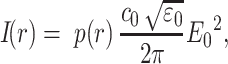
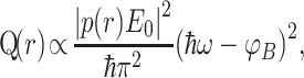
To quantitatively describe the correlation between the charge density and the plasmonic near-field intensity of the Au NDs/TiO2 ( ), we calculated the square of the near-field intensity enhancement (
 , where
  is incident electric field intensity) distribution of the Au NDs/TiO2 nanostructure under horizontal polarized light irradiation (Fig. 3a). Plasmonic near-field coupling intensity at the nanogap was significantly enhanced with decreasing interparticle distance. To intuitively evaluate the enhancement in the density of spatially separated holes, we defined an SPV enhancement factor (EF) as the ratio between the SPV magnitudes detected at Au NDs/TiO2 interface inside the nanogap (P1) and outside of the dimer (P2), as shown in Fig. 3b. The SPV EF shows an inverse dependence on the interparticle distance (Fig. 3c). The result is reminiscent of that of surface-enhanced Raman spectroscopy, which indicates that the Raman signal enhancement factor can be modified by changing the interparticle distance of the Au dimer [40]. To evaluate the correlation between the SPV and the local near-field intensity, the ratio of the near-field enhancement at P1 to that at P2 for Au NDs with different distances was calculated according to the line profiles of the near-field distribution (Supplementary Fig. 17). Interestingly, the decay trend of the SPV EF versus interparticle distance coincides with that of the square of the enhanced near-field intensity, indicating that the density of the spatially separated holes is proportional to the square of the amplitude of the enhanced near-field. This qualitative relationship is supported by the quantum theory in metal NPs [41,42]. Considering a monochromatic plane–wave interaction with the Au NDs/TiO2 nanostructure, the optical field intensity at the sample surface can be written as follows:
 |
(1) |
where r is arbitrary spatial location on Au ND/TiO2 surface, p(r) is the amplification magnitude of the local optical field at an arbitrary position in space,  is the optical dielectric constant of air,
  is a constant and
  is the incident electric field intensity. From the theory based on the equation of motion of the density matrix and the Fowler law for electron injection probability [41], the number of injected electrons or remaining holes is obtained as follows:
 |
(2) |
where  describes the amount of spatially separated charge resulting from plasmon-induced interfacial charge transfer, which is directly correlated with the SPV signal. Thus, the SPV signal can be conveniently expressed in terms of the electric field as follows:
 |
(3) |
which is consistent with the experimental observation (Fig. 3c). According to the aforementioned consideration, plasmonic optical antenna with multiple hot spots can create a high density of photogenerated charges, which is the prerequisite for multi-charge involved photocatalytic oxidation reactions, in particular, for the water oxidation reaction.
Figure 3.
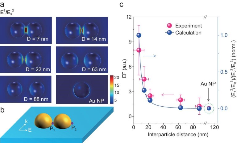
Spatial distribution of the calculated near-field enhancement and the experimental SPV EF of Au NP/TiO2 and Au dimers/TiO2 with varying gap distance (D). (a) Spatial distribution of the calculated near-field intensity enhancement (defined as  ) at plasmon resonance excitation. (b) Schematic of the definition of P1 and P2. P1 corresponds to the Au NDs/TiO2 interface in the nanogap region, and P2 corresponds to the region of the Au NDs/TiO2 extremities. (c) SPV EF and the square of the calculated near-field intensity enhancement of Au NP/TiO2 and Au NDs/TiO2 as a function of the dimer interparticle distance. E1 and E2 correspond to the electric field intensity at P1 and P2, respectively. Error bars in the plots indicate the statistical uncertainty of the SPV.
Among the most challenging and important photocatalytic reactions, water oxidation is regarded as the primary reaction for natural and artificial photosynthesis. Water oxidation involves successive oxidation of intermediates, which needs to accumulate sufficient holes at reaction sites to effectively drive the multi-hole transfer processes [16]. Such a reaction is particularly suitable to verify the critical role played by the surface-accumulating hole in a catalytic reaction. Plasmonic holes have been demonstrated to be capable of achieving water oxidation at the Au NPs/TiO2 interface under visible light [13]. Theoretical simulations indicated that the rate-determining step for oxygen evolution is the generation of *OOH intermediate with an activation energy barrier of ∼3.0 eV [13]. The highly oxidized intermediate requires the next transport of hole from reaction center to generate oxygen molecule within a short time. The local charge density at reaction sites thus plays a critical role for efficient water oxidation. Here, Au NDs/TiO2 samples possess notable superiority in tuning hole density at hot spots by varying the interparticle distance. Thus, we used visible-light-driven water oxidation as a probe reaction to elucidate the effect of hole density at hot spots on the reaction. The scanning electron microscopy (SEM) image in Fig. 4a shows Au NPs dispersed on TiO2 film, but the interparticle distance exceeds 100 nm, suggesting the absence of plasmon-coupling effect in this sample. To verify whether plasmon coupling of Au NDs is favorable for reaction activity enhancement, Au NDs/TiO2 samples were prepared using DNA super-origami as templates (see details in Supplementary data; Supplementary Fig. 18). Figure 4b and c show the SEM images of the Au NDs/TiO2 sample with a separation distance of 36 nm (signed as Au ND/TiO2-36) and 26 nm (signed as Au ND/TiO2-26), which is within the scope of the plasmon coupling but with a weak coupling according to Fig. 3c. When the Au ND separation distance was further decreased to 10 nm (signed as Au ND/TiO2-10) (Fig. 4d), the plasmon coupling strength greatly increased. Since the local density of accumulating plasmonic holes at hot spots of coupled Au ND/TiO2 photocatalyst is lower than the generally recognized inflection point (1 nm−2) from first- to third-order reaction mechanism for water oxidation [43], we consider the rate-determining step for water oxidation remains unchanged under coupling effect. It is thus anticipated that more plasmonic holes will accumulate at the Au NDs/TiO2 interface for effectively triggering the water oxidation reaction.
Figure 4.

Architecture and photoelectrochemical performance of plasmonic photoanodes. (a–d) SEM images of Au NP/TiO2 and Au NDs/TiO2 photoanodes. The insets show the schematics of the plasmonic samples. (e) Schematic of the photoelectrochemical measurement of an Au NDs/TiO2 electrode. (f) Current versus potential characteristics of plasmonic photoanodes recorded in a 1 M aqueous Na2SO4 solution under visible-light irradiation (>420 nm). (g) Photocurrent density of Au NP/TiO2 and Au NDs/TiO2 photoelectrodes at a fixed applied potential of 0.5 V versus Ag/AgCl.
Photoelectrochemical (PEC) water oxidation performance of Au NDs/TiO2 photoanodes under visible-light irradiation (λ > 420 nm) were examined in a three-electrode cell with Pt foil as the counter electrode and Ag/AgCl as the reference electrode (Fig. 4e). The surface coverage of Au nanoparticles for all samples used in photoelectrochemical experiments is 2%. As displayed in Fig. 4f, Au NDs/TiO2 samples significantly outperform Au NPs/TiO2 in PEC water oxidation under potentials from 0.1 to 1.0 VAg/AgCl. As the separation distance of Au dimers decreased, photocurrent density is dramatically increased due to the strong plasmon coupling. The negative shift of onset potential of the Au ND/TiO2-10 sample can be attributed to the extreme high density of plasmonic holes accumulated at the reaction site. Chopped photocurrent–time curves show that the steady photocurrents of the Au NDs/TiO2-10 is up to 0.46 μA/cm2 at 0.5 VAg/AgCl, which is higher than that of Au NPs/TiO2 (0.05 μA/cm2) (Supplementary Fig. 19a). It should be noted that the photocurrent density of the Au NDs/TiO2 sample for water oxidation is low, which is attributed to low surface coverage of Au dimers. Moreover, there is no photocurrent observed for the Au-free/TiO2 sample, suggesting that the enhanced photocatalytic activity was induced by plasmonic effect. To verify the production of O2 molecules, the concentration of dissolved oxygen was monitored with fluorescence-based O2 sensor for Au NDs/TiO2-10 over one hour (Supplementary Fig. 19b). The concentration is increased with prolonging photocatalytic reaction time. Figure 4g provides the quantitative correlation between the water oxidation activity and the Au ND separation distance. Au NPs/TiO2 can also initiate water oxidation reaction and show the least activity. For Au NDs/TiO2 electrode, the water oxidation activity is greatly enhanced and its activity is further enhanced when the separation distance is shortened from 36 to 10 nm. Photocurrent density of Au NDs/TiO2-10 for plasmon-induced water oxidation is about one order of magnitude higher compared with the Au NP/TiO2 photoanode, following the relationship between SPV EF and separation distance recognized in the experiment (Fig. 3c).
Photocurrent shows the dependence on excitation wavelength and the action spectrum qualitatively tracks the SPR absorption spectrum of the Au ND/TiO2 sample (Supplementary Fig. 20a), which convincingly demonstrates that the surface plasmonic effect is responsible for the observed water oxidation activity. Electrochemical impedance spectroscopy (EIS) measurements show a smaller arc radius of Au ND/TiO2-10 compared to the Au NP/TiO2 sample (Supplementary Fig. 21a and Table S1), demonstrating that plasmon coupling effect can also facilitate the charge transfer process from Au ND/TiO2 to redox species. Open circuit photovoltage (OCP) analysis further demonstrates that plasmon coupling of Au NDs plays a critical role in the density of accumulated charges for water oxidation (Supplementary Fig. 21b). The observed linear dependence of catalytic activities and the SPV on the light intensity for Au/TiO2 also indicates that the high density of holes accumulated at the reaction site is favorable for the water oxidation reaction (Supplementary Figs 6 and 21). These results show that multiple holes accumulated at plasmonic photocatalyst reaction sites play a crucial role during water oxidation. Au ND/TiO2 exhibited good stability within 300 s, and photocurrent decreased with increasing time due to the amplification of separation distance of Au dimers (Supplementary Fig. 22).
CONCLUSION
In conclusion, we demonstrated a plasmonic coupling effect in Au NDs/TiO2 that provides intense near-field at its interface in the nanogap region, enabling a high density of spatially separated holes accumulated at hot spots, as proven by the enhanced SPV signal. We showed that it is possible to tune the local charge density by varying the separation distance, light polarization and illumination wavelength. By combining these results with theoretical simulation, we further determined the quantitative relationship between the local charge density and near-field enhancement. We further explored the effect of the local charge accumulation of the Au NDs/TiO2 on the multi-hole driven water oxidation reaction and observed nearly one order of magnitude enhancement in the catalytic activity compared to that of the Au NP/TiO2 sample. Thus, as well as identifying the spatial sites of charge ‘hot spots’, the results demonstrated that the plasmonic coupling effect in a metal/semiconductor nanostructure generates a previously unrecognized effect on accumulating charge for a multi-electron/hole catalytic reaction. This study provides insight into the extraction and management of charge in a plasmonic photocatalytic system.
METHODS
Fabrication of Au NP/TiO2 and Au dimers/TiO2 nanostructure
Au NPs solution was prepared according to the literature [44]. Au NPs were then deposited on Nb-rutile (100) crystal (0.05 wt% Nb-doped, 10 × 10 × 0.5 mm, Shinkosha) using spin-coating method. Before KPFM measurements, the Au NPs/TiO2 was exposed to O2 plasma and thermal treatment. A detailed description of this process is available in Supplementary data. Au dimers solution was synthesized using super-origami as templates for anchoring Au NPs through DNA hybridization [45]. For PEC measurements, Au dimers were deposited on TiO2 film by adsorption 15 min. TiO2 thin films were deposited onto the indium tin oxide substrate using a chamber-type Atomic Layer Deposition reactor (home built). A detailed description of this process is available in Supplementary data.
Characterization
SEM images were taken using a field-emission scanning electron microscope (FE-SEM, JEOL JSM-7800F) at an operating voltage of 20 kV. High-resolution transmission electron microscopy (HR-TEM) images were obtained on a FEI Tecnai G2 F30 S-Twin (FEI Company) with an accelerating voltage of 300 kV for measuring the Au NP sizes. X-ray photoelectron spectroscopy (XPS) measurements were performed on a VG ESCALAB MK2 spectrometer with monochromatized Al-Kα excitation.
KPFM measurement
Surface potential of the samples were measured using an amplitude-modulated (AM) KPFM (Bruker Dimension V SPM system) in a dual-scan technique. The recorded signals of topography and surface potential arise from their respective retrace scanning processes, reducing the risk of cross-talk effects between the topography and surface potential channels. Surface photovoltage (SPV) was the difference in surface potential under illumination and in the dark, which directly related to the photogenerated charge distribution with nanometer spatial resolution. The test parameters and detailed description of this process is available in Supplementary data.
PEC measurement
PEC measurements were performed in a three-electrode glass cell with a quartz window containing an aqueous solution of 1 M Na2SO4. Pt foil was used as the counter electrode and Ag/AgCl as the reference electrode. A 300-W Xenon lamp was used as the light source. A long-pass filter (>420 nm) was used to obtain visible light for PEC measurement. The fluorescence-based O2 sensor (Neofox, Ocean Optics) was used to test the dissolved oxygen in reaction solution. An N2-gas was used to purge the O2 of reaction solution before illumination.
Supplementary Material
Acknowledgements
We acknowledge the characterization support from the Testing Center at Dalian Institute of Chemical Physics, Chinese Academy of Sciences.
Contributor Information
Yuying Gao, State Key Laboratory of Catalysis, Dalian National Laboratory for Clean Energy, Collaborative Innovation Center of Chemistry for Energy Materials (iChEM), Dalian Institute of Chemical Physics, Chinese Academy of Sciences, Dalian 116023, China; University of Chinese Academy of Sciences, Beijing 100049, China.
Feng Cheng, State Key Laboratory of Catalysis, Dalian National Laboratory for Clean Energy, Collaborative Innovation Center of Chemistry for Energy Materials (iChEM), Dalian Institute of Chemical Physics, Chinese Academy of Sciences, Dalian 116023, China.
Weina Fang, School of Chemistry and Chemical Engineering, and Institute of Molecular Medicine, Renji Hospital, School of Medicine, Shanghai Jiao Tong University, Shanghai 200240, China.
Xiaoguo Liu, School of Chemistry and Chemical Engineering, and Institute of Molecular Medicine, Renji Hospital, School of Medicine, Shanghai Jiao Tong University, Shanghai 200240, China.
Shengyang Wang, State Key Laboratory of Catalysis, Dalian National Laboratory for Clean Energy, Collaborative Innovation Center of Chemistry for Energy Materials (iChEM), Dalian Institute of Chemical Physics, Chinese Academy of Sciences, Dalian 116023, China.
Wei Nie, State Key Laboratory of Catalysis, Dalian National Laboratory for Clean Energy, Collaborative Innovation Center of Chemistry for Energy Materials (iChEM), Dalian Institute of Chemical Physics, Chinese Academy of Sciences, Dalian 116023, China; University of Chinese Academy of Sciences, Beijing 100049, China.
Ruotian Chen, State Key Laboratory of Catalysis, Dalian National Laboratory for Clean Energy, Collaborative Innovation Center of Chemistry for Energy Materials (iChEM), Dalian Institute of Chemical Physics, Chinese Academy of Sciences, Dalian 116023, China.
Sheng Ye, State Key Laboratory of Catalysis, Dalian National Laboratory for Clean Energy, Collaborative Innovation Center of Chemistry for Energy Materials (iChEM), Dalian Institute of Chemical Physics, Chinese Academy of Sciences, Dalian 116023, China.
Jian Zhu, State Key Laboratory of Catalysis, Dalian National Laboratory for Clean Energy, Collaborative Innovation Center of Chemistry for Energy Materials (iChEM), Dalian Institute of Chemical Physics, Chinese Academy of Sciences, Dalian 116023, China.
Hongyu An, State Key Laboratory of Catalysis, Dalian National Laboratory for Clean Energy, Collaborative Innovation Center of Chemistry for Energy Materials (iChEM), Dalian Institute of Chemical Physics, Chinese Academy of Sciences, Dalian 116023, China.
Chunhai Fan, School of Chemistry and Chemical Engineering, and Institute of Molecular Medicine, Renji Hospital, School of Medicine, Shanghai Jiao Tong University, Shanghai 200240, China.
Fengtao Fan, State Key Laboratory of Catalysis, Dalian National Laboratory for Clean Energy, Collaborative Innovation Center of Chemistry for Energy Materials (iChEM), Dalian Institute of Chemical Physics, Chinese Academy of Sciences, Dalian 116023, China.
Can Li, State Key Laboratory of Catalysis, Dalian National Laboratory for Clean Energy, Collaborative Innovation Center of Chemistry for Energy Materials (iChEM), Dalian Institute of Chemical Physics, Chinese Academy of Sciences, Dalian 116023, China.
FUNDING
This work was supported by the National Natural Science Foundation of China (21633015 and 21773228), the Chinese Academy of Sciences Interdisciplinary Innovation Team (JCTD-2018–10), Dalian Institute of Chemical Physics Innovation Foundation (DICPSZ201801) and the Strategic Priority Research Program and Equipment Development Project of the Chinese Academy of Sciences (XDB17000000 and YJKYYQ20170002).
AUTHOR CONTRIBUTIONS
Y.-Y.G. performed the experiments and wrote the manuscript. F.C. performed the theoretical calculations. W.-N.F. and X.-G.L. synthesized the Au dimer nanostructure. S.-Y.W. synthesized Au nanoparticle solution. J.Z. and F.-T.F. set up the KPFM experimental apparatus. W.N., R.-T.C. and H.-Y.A. performed the analysis of the KPFM measurements. S.Y. carried out electrochemical experiments. C.-H.F., F.-T.F. and C.L. analyzed data and revised the manuscript. C.L. conceived the research project. All the authors discussed the results and commented on the manuscript.
Conflict of interest statement. None declared.
REFERENCES
- 1. Shi X, Ueno K, Oshikiri Tet al. Enhanced water splitting under modal strong coupling conditions. Nat Nanotechnol 2018; 13: 953–8. [DOI] [PubMed] [Google Scholar]
- 2. Atwater HA, Polman A. Plasmonics for improved photovoltaic devices. Nat Mater 2010; 9: 205–13. [DOI] [PubMed] [Google Scholar]
- 3. Aslam U, Chavez S, Linic S. Controlling energy flow in multimetallic nanostructures for plasmonic catalysis. Nat Nanotechnol 2017; 12: 1000–5. [DOI] [PubMed] [Google Scholar]
- 4. Mubeen S, Lee J, Singh Net al. An autonomous photosynthetic device in which all charge carriers derive from surface plasmons. Nat Nanotechnol 2013; 8: 247–51. [DOI] [PubMed] [Google Scholar]
- 5. Clavero C. Plasmon-induced hot-electron generation at nanoparticle/metal-oxide interfaces for photovoltaic and photocatalytic devices. Nat Photon 2014; 8: 95–103. [Google Scholar]
- 6. Li JT, Cushing SK, Zheng Pet al. Plasmon-induced photonic and energy-transfer enhancement of solar water splitting by a hematite nanorod array. Nat Commun 2013; 4: 2651. [DOI] [PubMed] [Google Scholar]
- 7. Zrimsek AB, Chiang NH, Mattei Met al. Single-molecule chemistry with surface- and tip-enhanced Raman spectroscopy. Chem Rev 2017; 117: 7583–613. [DOI] [PubMed] [Google Scholar]
- 8. Ding SY, You EM, Tian ZQet al. Electromagnetic theories of surface-enhanced Raman spectroscopy. Chem Soc Rev 2017; 46: 4042–76. [DOI] [PubMed] [Google Scholar]
- 9. Christopher P, Moskovits M. Hot charge carrier transmission from plasmonic nanostructures. Ann Rev Phy Chem 2017; 68: 379–98. [DOI] [PubMed] [Google Scholar]
- 10. Zhou LA, Swearer DF, Zhang Cet al. Quantifying hot carrier and thermal contributions in plasmonic photocatalysis. Science 2018; 362: 69–72. [DOI] [PubMed] [Google Scholar]
- 11. Christopher P, Xin HL, Linic S. Visible-light-enhanced catalytic oxidation reactions on plasmonic silver nanostructures. Nat Chem 2011; 3: 467–72. [DOI] [PubMed] [Google Scholar]
- 12. Nishijima Y, Ueno K, Kotake Yet al. Near-infrared plasmon-assisted water oxidation. J Phy Chem Lett 2012; 3: 1248–52. [DOI] [PubMed] [Google Scholar]
- 13. Wang SY, Gao YY, Miao Set al. Positioning the water oxidation reaction sites in plasmonic photocatalysts. J Am Chem Soc 2017; 139: 11771–8. [DOI] [PubMed] [Google Scholar]
- 14. Tachibana Y, Vayssieres L, Durrant JR. Artificial photosynthesis for solar water-splitting. Nat Photon 2012; 6: 511–8. [Google Scholar]
- 15. Yano J, Yachandra V. Mn4Ca cluster in photosynthesis: where and how water is oxidized to dioxygen. Chem Rev 2014; 114: 4175–205. [DOI] [PMC free article] [PubMed] [Google Scholar]
- 16. Wang D, Sheng T, Chen JFet al. Identifying the key obstacle in photocatalytic oxygen evolution on rutile TiO2. Nat Catal 2018; 1: 291–9. [Google Scholar]
- 17. Corby S, Francas L, Selim Set al. Water oxidation and electron extraction kinetics in nanostructured tungsten trioxide photoanodes. J Am Chem Soc 2018; 140: 16168–77. [DOI] [PubMed] [Google Scholar]
- 18. Croce R, van Amerongen H. Natural strategies for photosynthetic light harvesting. Nat Chem Biol 2014; 10: 492–501. [DOI] [PubMed] [Google Scholar]
- 19. Zhang YC, He S, Guo WXet al. Surface-plasmon-driven hot electron photochemistry. Chem Rev 2018; 118: 2927–54. [DOI] [PubMed] [Google Scholar]
- 20. Wu K, Chen J, McBride JRet al. Efficient hot-electron transfer by a plasmon-induced interfacial charge-transfer transition. Science 2015; 349: 632–5. [DOI] [PubMed] [Google Scholar]
- 21. Jiang RB, Li BX, Fang CHet al. Metal/semiconductor hybrid nanostructures for plasmon-enhanced applications. Adv Mater 2014; 26: 5274–309. [DOI] [PubMed] [Google Scholar]
- 22. Harutyunyan H, Martinson AB, Rosenmann Det al. Anomalous ultrafast dynamics of hot plasmonic electrons in nanostructures with hot spots. Nat Nanotechnol 2015; 10: 770–4. [DOI] [PubMed] [Google Scholar]
- 23. Brown AM, Sundararaman R, Narang Pet al. Nonradiative plasmon decay and hot carrier dynamics: effects of phonons, surfaces, and geometry. ACS Nano 2016; 10: 957–66. [DOI] [PubMed] [Google Scholar]
- 24. Manjavacas A, Liu JG, Kulkarni Vet al. Plasmon-induced hot carriers in metallic nanoparticles. ACS Nano 2014; 8: 7630–8. [DOI] [PubMed] [Google Scholar]
- 25. Ishida T, Tatsuma T. Effect of plasmon coupling on quantum efficiencies of plasmon-induced charge separation. J Phy Chem C 2018; 122: 26153–9. [Google Scholar]
- 26. Kong XT, Wang ZM, Govorov AO. Plasmonic nanostars with hot spots for efficient generation of hot electrons under solar illumination. Adv Opt Mater 2017; 5: 1600594. [Google Scholar]
- 27. Chen Q, Mao L, Li Yet al. Quantitative operando visualization of the energy band depth profile in solar cells. Nat Commun 2015; 6: 7745. [DOI] [PMC free article] [PubMed] [Google Scholar]
- 28. Zhu J, Fan FT, Chen RTet al. Direct imaging of highly anisotropic photogenerated charge separations on different facets of a single BiVO4 photocatalyst. Angew Chem Int Ed 2015; 54: 9111–4. [DOI] [PubMed] [Google Scholar]
- 29. Chen RT, Pang S, An HYet al. Charge separation via asymmetric illumination in photocatalytic Cu2O particles. Nat Energy 2018, 3: 655–63. [Google Scholar]
- 30. Gao YY, Zhu J, An HYet al. Directly probing charge separation at interface of TiO2 phase junction. J Phy Chem Lett 2017; 8: 1419–23. [DOI] [PubMed] [Google Scholar]
- 31. Sivun D, Vidal C, Munkhbat Bet al. Anticorrelation of photoluminescence from gold nanoparticle dimers with hot-spot intensity. Nano Lett 2016; 16: 7203–9. [DOI] [PMC free article] [PubMed] [Google Scholar]
- 32. Kronik L, Shapira Y. Surface photovoltage phenomena: theory, experiment, and applications. Surf Sci Rep 1999; 37: 1–206. [Google Scholar]
- 33. Osterloh FE. Nanoscale effects in water splitting photocatalysis. In: Tüysüz H, Chan CK (eds). Solar Energy for Fuels. Berlin: Springer, 2016, 105–42. [DOI] [PubMed] [Google Scholar]
- 34. Strassburg E, Boag A, Rosenwaks Y. Reconstruction of electrostatic force microscopy images. Rev Sci Instrum 2005; 76: 083705. [Google Scholar]
- 35. Tumkur TU, Yang X, Cerjan Bet al. Photoinduced force mapping of plasmonic nanostructures. Nano Lett 2016; 16: 7942–9. [DOI] [PubMed] [Google Scholar]
- 36. Gwo S, Chen HY, Lin MHet al. Nanomanipulation and controlled self-assembly of metal nanoparticles and nanocrystals for plasmonics. Chem Soc Rev 2016; 45: 5672–716. [DOI] [PubMed] [Google Scholar]
- 37. Junno T, Deppert K, Montelius Let al. Controlled manipulation of nanoparticles with an atomic-force microscope. Appl Phys Lett 1995; 66: 3627–9. [Google Scholar]
- 38. Rechberger W, Hohenau A, Leitner Aet al. Optical properties of two interacting gold nanoparticles. Opt Commun 2003; 220: 137–41. [Google Scholar]
- 39. Jain PK, Huang W, El-Sayed MA. On the universal scaling behavior of the distance decay of plasmon coupling in metal nanoparticle pairs: a plasmon ruler equation. Nano Lett 2007; 7: 2080–8. [Google Scholar]
- 40. Kusch P, Mastel S, Mueller NSet al. Dual-scattering near-field microscope for correlative nanoimaging of SERS and electromagnetic hotspots. Nano Lett 2017; 17: 2667–73. [DOI] [PubMed] [Google Scholar]
- 41. Govorov AO, Zhang H, Gun’ko YK. Theory of photoinjection of hot plasmonic carriers from metal nanostructures into semiconductors and surface molecules. J Phy Chem C 2013; 117: 16616–31. [Google Scholar]
- 42. Govorov AO, Zhang H, Demir HVet al. Photogeneration of hot plasmonic electrons with metal nanocrystals: quantum description and potential applications. Nano Today 2014; 9: 85–101. [Google Scholar]
- 43. Mesa CA, Francas L, Yang KRet al. Multihole water oxidation catalysis on haematite photoanodes revealed by operando spectroelectrochemistry and DFT. Nat Chem 2020; 12: 82–9. [DOI] [PubMed] [Google Scholar]
- 44. Li JF, Tian XD, Li SBet al. Surface analysis using shell-isolated nanoparticle-enhanced Raman spectroscopy. Nat Protoc 2013; 8: 52–65. [DOI] [PubMed] [Google Scholar]
- 45. Fang WN, Jia SS, Chao Jet al. Quantizing single-molecule surface-enhanced Raman scattering with DNA origami metamolecules. Sci Adv 2019; 5: 4506. [DOI] [PMC free article] [PubMed] [Google Scholar]
Associated Data
This section collects any data citations, data availability statements, or supplementary materials included in this article.