

Abstract
WTe2, as a type-II Weyl semimetal, has 2D Fermi arcs on the (001) surface in the bulk and 1D helical edge states in its monolayer. These features have recently attracted wide attention in condensed matter physics. However, in the intermediate regime between the bulk and monolayer, the edge states have not been resolved owing to its closed band gap which makes the bulk states dominant. Here, we report the signatures of the edge superconductivity by superconducting quantum interference measurements in multilayer WTe2 Josephson junctions and we directly map the localized supercurrent. In thick WTe2 ( , the supercurrent is uniformly distributed by bulk states with symmetric Josephson effect (
 ). In thin WTe2 (10 nm), however, the supercurrent becomes confined to the edge and its width reaches up to
  and exhibits non-symmetric behavior
  . The ability to tune the edge domination by changing thickness and the edge superconductivity establishes WTe2 as a promising topological system with exotic quantum phases and a rich physics.
Keywords: WTe2, Josephson junction, Weyl semimetal, edge superconductivity, non-symmetric effect
We report the evidence of edge superconductivity in multilayer WTe2 Josephson junctions which remains rarely studied in type-II Weyl semimetal.
INTRODUCTION
Layered WTe2 was suggested as the first material candidate to be a type-II Weyl semimetal, where eight separated Weyl points exist in the bulk and topological Fermi arcs occur on the (001) crystal surfaces owing to the reflection symmetry [1]. An extra set of quantum oscillations arising from Weyl orbits were observed as evidence of Fermi arcs in transport [2]. Intriguingly, when the thickness is reduced to the monolayer, WTe2 turns to be a quantum spin Hall insulator with edge states [3], which have been demonstrated in numerous experiments involving low-temperature transport [4,5], angle-resolved photoelectron spectroscopy [6], scanning tunneling microscopy [7,8], and microwave impedance microscopy [9]. Besides, it has also been predicted that WTe2 has 1D hinge states as a higher-order topological insulator [10].
While the boundary modes of WTe2 have been well studied in both the 3D and 2D limits [11,12], in multilayers these modes become rather complicated due to the intervening bulk and edge states and thus they remain largely unexplored. Unlike the monolayer WTe2, the nearly-closed bandgap in multilayer WTe2 results in a large density of bulk states. Therefore, it is difficult to distinguish the edge states through a gating approach. It is then necessary to make them distinct from the coexisting bulk ones. However, separating edge and bulk states in a single electrical conductance measurement may be ambiguous. In contrast, if the charge carriers condense together to form Cooper pairs, the difference can be amplified since the supercurrent properties are largely related to the coherence length [13]. A planar microscopic Josephson junction to realize superconducting TSM is feasible to elucidate the boundary states. For example, in Nb/Bi2Te3/Nb Josephson junctions the surface states enable the ballistic Josephson current rather than the diffusive bulk transport [14]. The supercurrent distribution in real space can be also quantitatively extracted from the superconducting quantum interference (SQI) measurements, where a perpendicular magnetic field induces oscillations in the amplitude of the superconducting current in Josephson junctions. This approach has been widely adopted to reveal the quantum spin Hall edge states in HgTe quantum well [15], topological surface states in TI [16] and quantum Hall edge states in graphene [17], but not yet in TSM.
Here, we report the observation of edge superconductivity in multilayer WTe2 Josephson junctions. By varying the thickness of WTe2 in SQI experiments, we have observed the Fraunhofer and the mixture of Fraunhofer and SQUID pattern in thick and thin WTe2, respectively, which indicates the edge superconductivity in thin WTe2. The non-uniform supercurrent exists in multilayer WTe2 up to 16 nm, while the bulk supercurrent density amplitude ( ) is about
  of the edge in the thinnest sample.
  is also observed in thin WTe2 due to the inversion symmetry breaking.
WTe2 JOSEPHSON JUNCTIONS
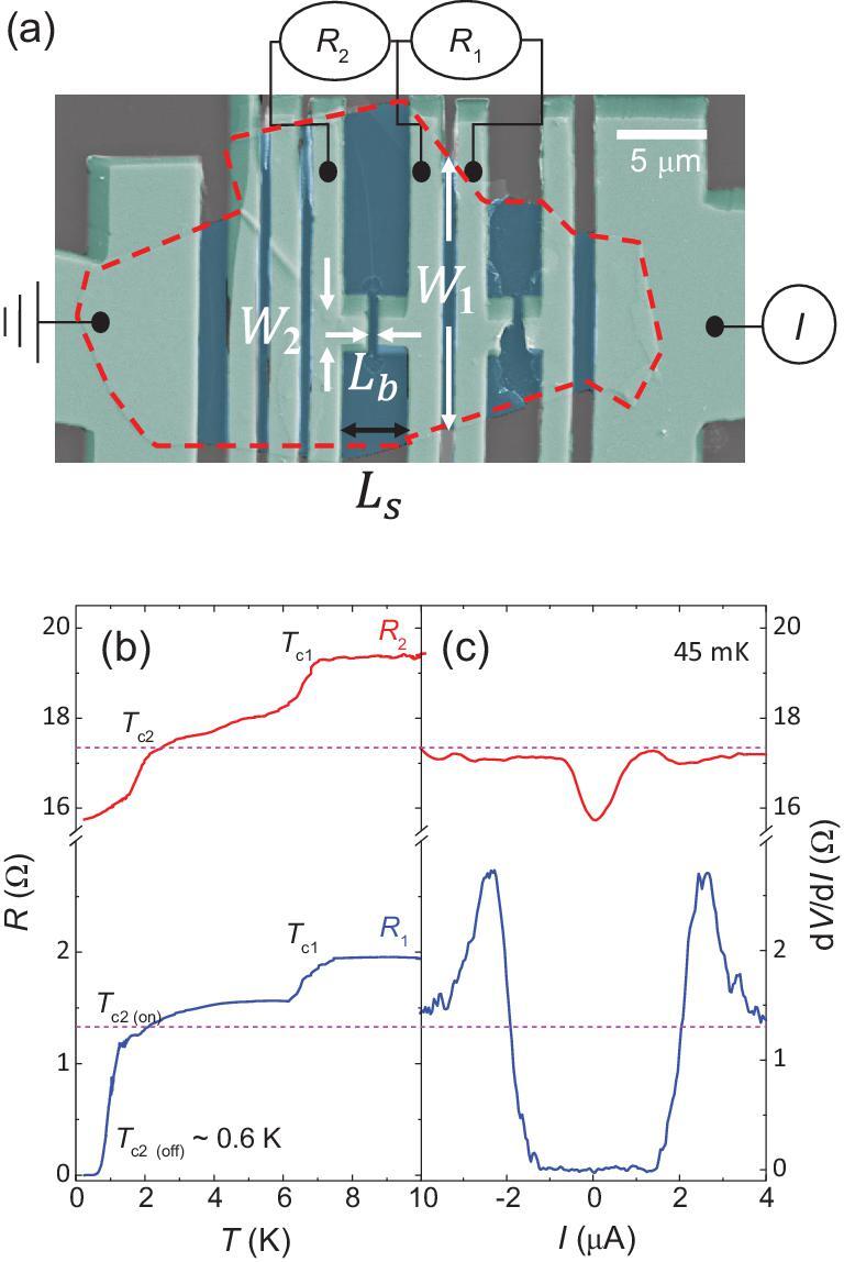
We measure several Josephson junctions consisting of WTe2 flakes of different thicknesses contacted by niobium (Nb) leads. The fabrication and characterization details are described in the Methods and SI Section I (Supplementary Figs 1 and 2). A scanning electron microscopy (SEM) image of the actual device and its measurement configuration are displayed in Fig. 1a (device #1, 10 nm-thick WTe2). The length and width of the superconducting channel are  and
and  respectively. Figure 1b shows the resistance-temperature (R-T) curve of the junction with two transitions
  and
and  at zero magnetic field.
  originates from the Nb superconducting transition, while the resistance continues to drop to
  times of the normal resistance below
  which comes from the proximity Josephson coupling. The Josephson effect is highly reproducible across different devices, as shown in Supplementary Fig. 3. Figure 1c and its inset display the I-V characteristics and the differential resistance (
 ) of the junction at 45 mK, respectively. From the slope of the I-V curve in the high bias region (
 ) where the curve is linear, the normal-state resistance
  is extracted. For
  , the voltage and
  across the junction remain nearly zero, indicating a robust Josephson effect. Ten WTe2 Josephson junctions with various
  and
and  are studied (see Table S1 for their junction parameters), all exhibiting a finite supercurrent at low temperatures with reproducible behavior. The junction is in the long junction limit [18] (see SI Section IV and Supplementary Fig. 4 for details). Therefore it follows the
  dependence found from the
  plot versus L in Fig. 1d. In this long junction regime, the critical current is given [18,19] by
  being determined by the Thouless energy
  , which can be estimated [20] to be
  , yielding
  .
.
Figure 1.

Josephson effect in thin WTe2. (a) Top: Junctions schematic. Bottom: False-colour SEM image of the device with the measurement configuration. 120 nm-thick Nb is deposited on the top of WTe2 (device #1). A four-terminal measurement across the interface was performed. The in-plane crystal axis of the WTe2 flake is unknown. (b) Temperature dependence of WTe2 Josephson junction resistance. Two transitions are identified:  is from the superconducting Nb,
  is from the proximity Josephson coupling of WTe2. Inset shows that the junction has a length of
  (c) I-V characteristics for Josephson junction in the superconducting states with a critical current of
  under zero magnetic field at 45 mK. Inset: dV/dI characteristics indicate zero resistance below the critical current, the same as the I-V curve. (d) Effect of the junction length on supercurrent for eight devices. The product
  follows a general trend of
  .
.
THE SUPERCONDUCTING QUANTUM INTERFERENCE MEASUREMENTS
Having established the Josephson effect in our Nb/WTe2/Nb junctions, we then focus on the supercurrent of WTe2. In our experiments, the spatial distribution of the supercurrent is analyzed by applying a perpendicular magnetic field B during the SQI measurements with different thicknesses of WTe2. The particular shape of the critical current interference pattern depends on the phase-sensitive summation of the supercurrents traversing the junction. In the case of a symmetric supercurrent distribution, this integral takes the simple form [21]:
 |
where  is the effective length of the junction along the direction of the current, accounting for the magnetic flux threading [22] through parts of the superconducting contacts over the London penetration depths.
  corresponds to the magnetic flux quantum.
In thick WTe2, the bulk states dominate and along the y-axis the supercurrent density has an approximately uniform distribution as shown in Fig. 2a. Thus, the uniform current density yields the single-slit Fraunhofer pattern described by [21]
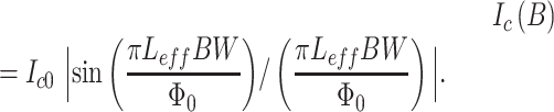 |
Figure 2.

Evolution of edge superconductivity in thin WTe2. (a) A schematic picture of a lateral Josephson junction with the out-of-plane magnetic field in thick WTe2. The thick WTe2 is filled with charge carriers and the supercurrent can flow uniformly across the junction along the y-axis, corresponding to a flat supercurrent density  . (b) The differential resistance at different values of
  in 60 nm-thick WTe2 (device #8), showing the single-slit interference characteristics with a uniform supercurrent density. (c) The supercurrent distribution along the y-axis, which is calculated by the inverse Fourier transform of the data in (b). The supercurrent density is uniform along the y-axis, consistent with trivial bulk charge transport. (d) Critical current
  as a function of B for the two sweep directions (positive as the blue line, negative as the red line). Two curves overlap with each other. (e) A schematic picture of a lateral Josephson junction with the out-of-plane magnetic field where
  denotes the pairing order parameter of two superconducting Nb electrodes. In thin WTe2, the bulk domination decreases and the supercurrent is carried by the edge. The edges on two sides of WTe2 have different Fermi velocities
  and
and  when the inversion symmetry is broken that gives rise to the asymmetric Josephson effect. (f) Differential resistance across the 13 nm-thick WTe2 junction (device #2), showing a mixture of Fraunhofer and SQUID-like pattern with a central lobe of width
  and side lobes of width
  . The black line shows the fitting results from the edge-stepped supercurrent model. (g) The supercurrent distribution of device #2. The widths of the supercurrent-carrying edge channels are estimated to be
  (h) Critical current
  as a function of B for the two sweep directions (positive as the blue line, negative as the red line), indicating non-symmetric behavior
  .
.
We have measured device #8 with 60 nm-thick WTe2 as shown in Fig. 2b. The critical current envelope has an oscillation characteristic. We obtain a period of  , which yields the effective length of
  This effective length, larger than the distance between the two Nb electrodes (
 , is caused by the London penetration depth and the flux focusing due to the Meissner effect [23,24]. The critical current envelope strongly resembles a single-slit pattern with
  central lobe width. The corresponding supercurrent distribution is obtained by transforming the single-slit pattern to the real-space current density,
  , as shown in Fig. 2c. This suggests a nearly uniform supercurrent density throughout the y direction. The full details of the extraction procedure can be found in the SI section V and Supplementary Fig. 5. Furthermore, the critical currents overlap each other at different current directions as shown in Fig. 2d which indicates a symmetric Josephson effect with
  , where
  and
and  denote the sweep direction of the bias current and
  and
and  are the magnetic field directions.
When the WTe2 is thinned down to a few layers, the low bulk density of states coexists with the possible high density at edges as shown in Fig. 2e. The magnetic-field-dependent critical current envelope in a 13 nm-thick WTe2 device (device #2) demonstrates the periodic SQI with a  central lobe width (Fig. 2f).
  decays slowly which is distinct from the Fraunhofer pattern in Fig. 2b. We use an edge-stepped nonuniform supercurrent model to directly simulate the
  relation as shown by the black line in Fig. 2f (see the model details in SI Section VI and Supplementary Fig. 6). The good fit of both the magnitude and periodicity of
  indicates the nonuniform supercurrent in few-layer WTe2. Furthermore, the mixture of Fraunhofer and SQUID interference pattern corresponds to the development of sharp peaks in the supercurrent density at the mesa edges in Fig. 2g. The widths of the supercurrent-carrying edge are estimated to be in the range
  The value is similar to other edge superconductivity systems [15,25] and the additional edge modes or bulk modes coupled weakly to edge states across the junction to carry supercurrent can result in the large edge supercurrent channel. The relation of the critical current with the magnetic field is presented in Fig. 2h and behaves non-symmetric
  in most magnetic fields which is different with thick sample.
We have reproduced the edge superconductivity and the mixture of Fraunhofer and SQUID pattern in a 10 nm-thick WTe2 device (#1), and the traditional Fraunhofer pattern in a 40 nm-thick WTe2 device (#5, see SI Section VII and Supplementary Fig. 7 for details). The higher supercurrent density at edges suggests a robust coupling to the superconductor electrodes.
To further distinguish the superconducting proximity Josephson coupling of edge/bulk, we experiment with a 16 nm-thick WTe2 device (#3) to distinguish the bulk and edge contributions. Two Josephson channels are fabricated as the edge-crossing ( ) and edge-untouched (
 ) as shown in Fig. 3a. For
  , the junction is easier to be conducted by the bulk because the electrodes are closer in the central region (
 while far at the edge. The distance on the edge side is
  that makes it hard to realize the Josephson effect through the edge region. Since the thickness is uniform in this sample, as indicated by the atomic force microscopy (AFM) measurement (Supplementary Fig. 2c and d), we can reasonably assume that the resistance by bulk states is isotropic and inversely proportional to the width. Figure 3b shows the R-T curve at low temperatures. Only edge-crossing
  can reach zero to exhibit Josephson effect while
  only decreases a little. The differential resistance versus the current measurement in Fig. 3c verifies this property. Since the lengths of two junctions differ slightly, the coherence length of
  should be larger than that of
  to realize the Josephson effect. A similar mixture of Fraunhofer and SQUID pattern with edge-dominated supercurrent is also observed, as shown in Supplementary Fig. 7b, which is consistent with the other two thin devices (#1 and #2). On the contrary,
  does not exhibit any oscillation and only the central lobe is observed (see Supplementary Fig. 8 for details). The width
  for
for  is estimated to be
  which corresponds well to the actual junction width
  as shown in Fig. 3a. The in-complete superconductivity of
  is due to the weaker superconducting combining for bulk. If the Josephson channel is further shortened, the bulk-only channel
  can also be superconducting in another device #9. However, only the Fraunhofer pattern with uniform supercurrent density is observed and corresponds well to the bulk-dominated sample #8 in Fig. 2c and d (see Figs S8 and 9 for details).
Figure 3.
The coupling of superconductor Nb to the bulk and edge WTe2 channels. (a) False-color SEM image of the device #3 with two measurement configurations.  and
and  represent the edge-crossing and edge-untouched junctions, respectively. The electrode separation width of
  from the edge
  is larger than
  The length for edge channel
  is
is  while for the bulk channel
  which makes the edge superconductivity hard to realize. (b) Temperature dependence of resistance in two junctions as shown in (a).
  is the superconducting transition of Nb while the superconducting WTe2 emerges at
  . (c) dV/dI characteristic at 45 mK.
DISCUSSION
It is necessary to discuss whether the observed edge superconductivity originates from the edge states in WTe2 or other trivial effects. All of the four different devices exhibit the sharp edge superconductivity which can exclude the accidental impurity effect. The exclusion of some trivial effects such as fluctuations and the affection by the SiO2 substrate and the capping layer in thinner WTe2 is also discussed in Supplementary Section VIII. However, it is difficult to exclude other trivial effects such as trivial edge states. Moreover, the other trivial mechanisms can also lead to a similar non-uniform supercurrent such as an inhomogeneous interface. A mixture of Fraunhofer and SQUID pattern was also observed in Nb-InGaAs/InP junctions with a step-shaped current density distribution [26]. Therefore, we need to point out that the edge superconductivity we observed is not equivalent to the superconductivity in the edge modes nor any evidence of toplogical superconducting phase. On the contrary, only the superconductivity in the edge region of samples can be concluded in our experiments.
The critical currents following  in thin WTe2 are quite interesting. In general, the asymmetric crystal can induce different Fermi velocities at two sides and result in supercurrent asymmetry. Since the supercurrent density is uniform as shown in Fig. 2c with symmetric Fraunhofer pattern (Fig. 2d), the bulk WTe2 does not contribute to the asymmetry. Consequently, this supercurrent asymmetry may be related to the edge which is consistent with the predicted effect of inversion-symmetry-breaking on Weyl semimetal [27]. The total Josephson current carried by the two edges can be described by [28]
 |
where  and
and  represent the Josephson current carried by the two edges,
  and
and  are the phase in WTe2 (the magnetic-field-related) and Nb regions (the current-related), respectively. The two edges have different energy spectra and
  in thin WTe2 (Fig. 2g) which results from different Fermi velocity of the two edge sides, denoted by the red and blue lines as shown in Fig. 2e. Therefore, the
  is not symmetric for both
  and
and  anymore. Other possibilities such as vortex trapping, vortex motion during the magnetic field sweep or bulk states asymmetry may contribute. However, the
  in the thick sample in Fig. 2d helps to largely exclude the other possibility.
We note that two recent preprints [29,30] have also studied WTe2 Josephson junction and shown evidence of edge states which is explained to be Hinge states [10]. Indeed, it is challenging to unambiguously determine the definite origin of edge superconductivity in our results, and various possibilities exist. However, from the consistent observations of high edge supercurrent density [29], the edge superconductivity is confirmed in the multi-layer WTe2 system. Compared to the reported data, we further perform thickness-dependence experiments and provide more evidence that edge superconductivity exists in thin WTe2 but not a thick one.
We summarize the supercurrent density amplitude ratio of the edge and bulk in Fig. 4. The edge superconductivity gradually emerges in thinner ones and the edge/bulk supercurrent amplitude reaches 2.76 in 10 nm-thick WTe2. The critical thickness for the transition from edge to bulk-dominated superconductivity is estimated to be  Moreover, various topological semimetals such as the TaAs family [31] (Fermi-arc surface states), layered MoTe2 [32] (edge states in the 2D limit) and ZrSiS [33] (nodal-line surface states) can be further fabricated into Josephson junctions to detect the surface/edge states.
Figure 4.
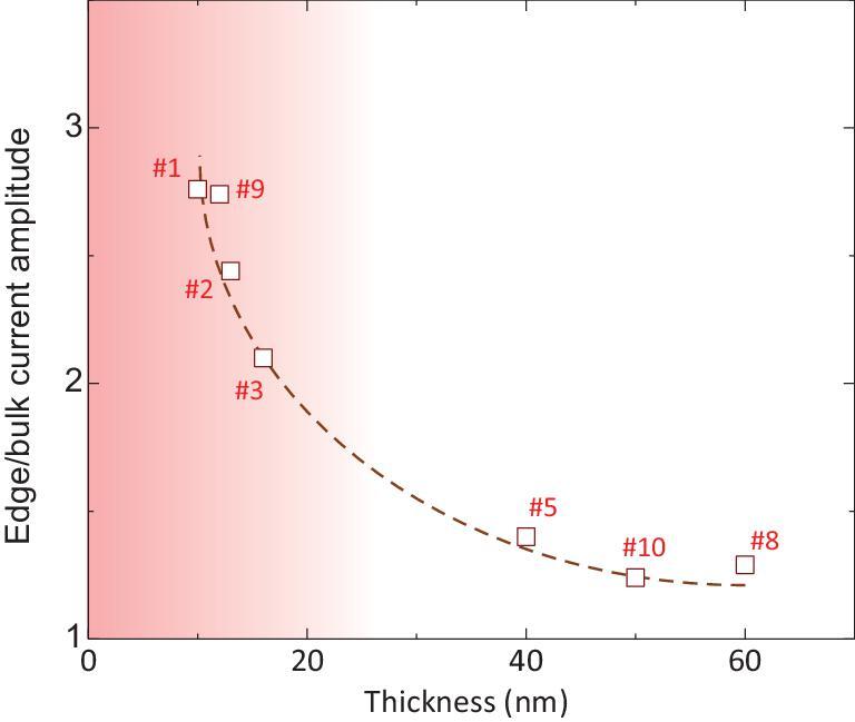
Summary of thickness-dependent edge-supercurrent-density contribution in WTe2. The edge/bulk current amplitude is estimated by the ratio of edge/bulk ( ) supercurrent density.
  and
and  are estimated by the average value of the left and right peaks and the value of the central region in position-dependent supercurrent density. The dashed line shows the trend.
CONCLUSION
In summary, by studying the Fraunhofer interference, our measurements provide the supercurrent distribution in type-II Weyl semimetal WTe2. In thin WTe2, the existence of edge superconductivity is evidenced. Besides, non-symmetric behavior  in WTe2 through the edge is an intrinsic property of the inversion symmetry breaking, which is distinct from other systems by an external in-plane magnetic field [22]. Furthermore, the Josephson junctions formed from 1D edge states or 2D surface states and s-wave superconducting contacts are expected to emulate spinless p-wave superconductivity [34] and Majorana flat bands [35] via a.c. Josephson effect by Shapiro response measurements. Edge superconductivity establishes WTe2 as a promising platform for the future realization of topological superconductivity and Majorana bound states.
METHODS
WTe2 crystal growth
High-quality bulk WTe2 crystals were grown by chemical vapor transport (CVT) method as reported before [36]. Single crystals of WTe2 were grown by a high-temperature self-flux method. High-purity tungsten powders (99.9%) and Te pieces (99.999%) were inserted into alumina crucibles with a molar ratio of 1:30 in a glove box filled with pure argon then sealed in quartz tubes under high vacuum. The tubes were heated to 1100°C in 20 hours and maintained for 10 hours. Then the furnace was slowly cooled down to 650°C with a rate of 2°C/h followed by separating the Te flux in a centrifuge at 650°C.
Device fabrication
The WTe2 flakes were mechanically exfoliated onto a Si substrate capped with a 280 nm-thick SiO2 layer and the thickness of WTe2 was identified by optical contrast and atomic force microscopy. The WTe2 Josephson junctions were fabricated by an e-beam lithography technique and wet-etched by standard buffered HF solution for 5 s in the electrode regime. We deposited 120 nm-thick Nb electrodes using magnetic sputtering. Then, 40 nm-thick SiO2 was deposited on top to prevent the WTe2 oxidization.
Transport measurements
Four-terminal temperature-dependent transport measurements were carried out in a Physical Property Measurement System (PPMS, Quantum Design) with a dilution refrigerator, which achieves a base temperature of 35 mK. The transport properties were acquired using lock-in amplifiers (SR830) and Agilent 2912 meters. We used an excitation current of <50 nA. In differential resistance (dV/dI) measurements, a small a.c. current bias (10 nA to 100 nA) is generated by the lock-in amplifier output voltage in combination with a 10  bias resistor. This small a.c. current is added on top of the larger d.c. current bias by Agilent 2912, and the induced differential voltage is measured using the lock-in technique with a low frequency (<50 Hz).
DATA AVAILABILITY
The data that support the plots within this paper and other findings of this study are available from the corresponding author upon reasonable request.
Supplementary Material
ACKNOWLEDGEMENTS
Part of the sample fabrication was performed at Fudan Nano-fabrication Laboratory. We thank Jinhui Shen from Prof. Xiaofeng Jin's group for help in the Nb metal deposition. We thank Liyang Qiu from Saijun Wu's group for help in Matlab code assistance. We thank Quansheng Wu for useful correspondence. We thank Prof. Kam Tuen Law from The Hong Kong University of Science and Technology for helpful discussion on the asymmetric behavior.
Contributor Information
Ce Huang, State Key Laboratory of Surface Physics and Department of Physics, Fudan University, Shanghai 200433, China; Collaborative Innovation Center of Advanced Microstructures, Nanjing 210093, China.
Awadhesh Narayan, SSCU, Indian Institute of Science, Bengaluru 560012, India.
Enze Zhang, State Key Laboratory of Surface Physics and Department of Physics, Fudan University, Shanghai 200433, China; Collaborative Innovation Center of Advanced Microstructures, Nanjing 210093, China.
Xiaoyi Xie, State Key Laboratory of Surface Physics and Department of Physics, Fudan University, Shanghai 200433, China; Collaborative Innovation Center of Advanced Microstructures, Nanjing 210093, China.
Linfeng Ai, State Key Laboratory of Surface Physics and Department of Physics, Fudan University, Shanghai 200433, China; Collaborative Innovation Center of Advanced Microstructures, Nanjing 210093, China.
Shanshan Liu, State Key Laboratory of Surface Physics and Department of Physics, Fudan University, Shanghai 200433, China; Collaborative Innovation Center of Advanced Microstructures, Nanjing 210093, China.
Changjiang Yi, Institute of Physics and Beijing National Laboratory for Condensed Matter Physics, Chinese Academy of Sciences, Beijing 100190, China.
Youguo Shi, Institute of Physics and Beijing National Laboratory for Condensed Matter Physics, Chinese Academy of Sciences, Beijing 100190, China; School of Physical Sciences, University of Chinese Academy of Sciences, Beijing 100190, China.
Stefano Sanvito, School of Physics, AMBER and CRANN Institute, Trinity College, Dublin 2, Ireland.
Faxian Xiu, State Key Laboratory of Surface Physics and Department of Physics, Fudan University, Shanghai 200433, China; Collaborative Innovation Center of Advanced Microstructures, Nanjing 210093, China; Institute for Nanoelectronic Devices and Quantum Computing, Fudan University, Shanghai 200433, China.
FUNDING
This work was supported by the National Key Research and Development Program of China (2017YFA0303302 and 2018YFA0305601), the Science and Technology Commission of Shanghai (19511120500), and the National Natural Science Foundation of China (61322407, 11934005, 11874116 and 61674040). A.N. acknowledges support from Indian Institute of Science. E.Z. acknowledges support from China Postdoctoral Innovative Talents Support Program.
AUTHOR CONTRIBUTIONS
F.X. conceived the ideas and supervised the overall research. Y.S. and C.Y. synthesized high-quality WTe2 bulk samples. C.H. and E.Z. fabricated the nanodevices. C.H., L.A. and S.L. carried out the PPMS measurements. A.N. and S.S. provided theoretical support. X.X. provided the curve fitting. C.H. and F.X. wrote the paper with assistance from all other authors.
Conflict of interest statement. None declared.
REFERENCES
- 1. Soluyanov AA, Gresch D, Wang Zet al. Type-II Weyl semimetals. Nature 2015; 527: 495–8. [DOI] [PubMed] [Google Scholar]
- 2. Li P, Wen Y, He Xet al. Evidence for topological type-II Weyl semimetal WTe2. Nat Commun 2017; 8: 2150. [DOI] [PMC free article] [PubMed] [Google Scholar]
- 3. Ok S, Muechler L, Di Sante Det al. Custodial glide symmetry of quantum spin Hall edge modes in monolayer WTe2. Phys Rev B 2019; 99: 121105. [Google Scholar]
- 4. Fei Z, Palomaki T, Wu Set al. Edge conduction in monolayer WTe2. Nat Phys 2017; 13: 677–82. [Google Scholar]
- 5. Wu S, Fatemi V, Gibson QDet al. Observation of the quantum spin Hall effect up to 100 kelvin in a monolayer crystal. Science 2018; 359: 76–9. [DOI] [PubMed] [Google Scholar]
- 6. Xu S-Y, Belopolski I, Alidoust Net al. Discovery of a Weyl fermion semimetal and topological fermi arcs. Science 2015; 349: 613–7. [DOI] [PubMed] [Google Scholar]
- 7. Tang S, Zhang C, Wong Det al. Quantum spin Hall state in monolayer 1T'-WTe2. Nat Phys 2017; 13: 683–7. [Google Scholar]
- 8. Collins JL, Tadich A, Wu Wet al. Electric-field-tuned topological phase transition in ultrathin Na3Bi. Nature 2018; 564: 390–4. [DOI] [PubMed] [Google Scholar]
- 9. Shi Y, Kahn J, Niu Bet al. Imaging quantum spin Hall edges in monolayer WTe2. Sci Adv 2019; 5: eaat8799. [DOI] [PMC free article] [PubMed] [Google Scholar]
- 10. Wang Z, Wieder BJ, Li Jet al. Higher-order topology, monopole nodal lines, and the origin of large fermi arcs in transition metal dichalcogenides XTe2(X = Mo,W). Phys Rev Lett 2019; 123: 186401. [DOI] [PubMed] [Google Scholar]
- 11. Shvetsov OO, Kononov A, Timonina AVet al. Realization of a Double-Slit SQUID geometry by fermi arc surface states in a WTe2 Weyl semimetal. JETP Lett 2018; 107: 774–9. [Google Scholar]
- 12. Shvetsov OO, Kononov A, Timonina AVet al. Subharmonic Shapiro steps in the a.c. Josephson effect for a three-dimensional Weyl semimetal WTe2. Europhys Lett 2018; 124: 47003. [Google Scholar]
- 13. Huang C, Zhou BT, Zhang Het al. Proximity-induced surface superconductivity in Dirac semimetal Cd3As2. Nat Commun 2019; 10: 2217. [DOI] [PMC free article] [PubMed] [Google Scholar]
- 14. Veldhorst M, Snelder M, Hoek Met al. Josephson supercurrent through a topological insulator surface state. Nat Mater 2012; 11: 417–21. [DOI] [PubMed] [Google Scholar]
- 15. Hart S, Ren H, Wagner Tet al. Induced superconductivity in the quantum spin Hall edge. Nat Phys 2014; 10: 638–43. [Google Scholar]
- 16. Lee JH, Lee G-H, Park Jet al. Local and nonlocal fraunhofer-like pattern from an edge-stepped topological surface josephson current distribution. Nano Lett 2014; 14: 5029–34. [DOI] [PubMed] [Google Scholar]
- 17. Amet F, Ke CT, Borzenets IVet al. Supercurrent in the quantum Hall regime. Science 2016; 352: 966–9. [DOI] [PubMed] [Google Scholar]
- 18. Dubos P, Courtois H, Pannetier Bet al. Josephson critical current in a long mesoscopic S-N-S junction. Phys Rev B 2001; 63: 064502. [Google Scholar]
- 19. Ben Shalom M, Zhu MJ, Fal’ko VIet al. Quantum oscillations of the critical current and high-field superconducting proximity in ballistic graphene. Nat Phys 2015; 12: 318–22. [Google Scholar]
- 20. Ishii C. Josephson currents through junctions with normal metal barriers. Prog Theor Phys 1970; 44: 1525–47. [Google Scholar]
- 21. Tinkham M. Introduction to Superconductivity. New York: McGraw-Hill, 1975. [Google Scholar]
- 22. Suominen HJ, Danon J, Kjaergaard Met al. Anomalous Fraunhofer interference in epitaxial superconductor-semiconductor Josephson junctions. Phys Rev B 2017; 95: 035307. [Google Scholar]
- 23. Paajaste J, Amado M, Roddaro Set al. Pb/InAs nanowire josephson junction with high critical current and magnetic flux focusing. Nano Lett 2015; 15: 1803–8. [DOI] [PubMed] [Google Scholar]
- 24. de Vries FK, Timmerman T, Ostroukh VPet al. h/e superconducting quantum interference through trivial edge states in InAs. Phys Rev Lett 2018; 120: 047702. [DOI] [PubMed] [Google Scholar]
- 25. Pribiag VS, Beukman AJA, Qu Fet al. Edge-mode superconductivity in a two-dimensional topological insulator. Nat Nanotechnol 2015; 10: 593–7. [DOI] [PubMed] [Google Scholar]
- 26. Schäpers T. Superconductor/Semiconductor Junctions. Julich: Springer, 2001. [Google Scholar]
- 27. Chen C, He JJ, Ali MNet al. Asymmetric Josephson effect in inversion symmetry breaking topological materials. Phys Rev B 2018; 98: 075430. [Google Scholar]
- 28. Asano Y, Tanaka Y, Sigrist Met al. Josephson current in s-wave-superconductor Sr2RuO4 junctions. Phys Rev B 2003; 67: 184505. [Google Scholar]
- 29. Choi Y-B, Xie Y, Chen C-Zet al. Evidence of higher-order topology in multilayer WTe2 from Josephson coupling through anisotropic hinge states. Nat Mater 2020; 12: doi:10.1038/s41563-020-0721-9. [DOI] [PubMed] [Google Scholar]
- 30. Kononov A, Abulizi G, Qu Ket al. One-dimensional states residing on edges and steps in few-layer WTe2. Nano Lett 2020; 20: 4228–33. [DOI] [PMC free article] [PubMed] [Google Scholar]
- 31. Lv BQ, Xu N, Weng HMet al. Observation of Weyl nodes in TaAs. Nat Phys 2015; 11: 724–7. [Google Scholar]
- 32. Deng K, Wan G, Deng Pet al. Experimental observation of topological Fermi arcs in type-II Weyl semimetal MoTe2. Nat Phys 2016; 12: 1105–10. [Google Scholar]
- 33. Liu J, Balents L.. Correlation effects and quantum oscillations in topological nodal-loop semimetals. Phys Rev B 2017; 95: 075426. [Google Scholar]
- 34. Fu L, Kane CL. Josephson current and noise at a superconductor/quantum-spin-Hall-insulator/superconductor junction. Phys Rev B 2009; 79: 161408. [Google Scholar]
- 35. Chen A, Pikulin DI, Franz M. Josephson current signatures of Majorana flat bands on the surface of time-reversal-invariant Weyl and Dirac semimetals. Phys Rev B 2017; 95: 174505. [Google Scholar]
- 36. Huang C, Narayan A, Zhang Eet al. Inducing strong superconductivity in WTe2 by a proximity effect. ACS Nano 2018; 12: 7185–96. [DOI] [PubMed] [Google Scholar]
Associated Data
This section collects any data citations, data availability statements, or supplementary materials included in this article.
Supplementary Materials
Data Availability Statement
The data that support the plots within this paper and other findings of this study are available from the corresponding author upon reasonable request.