

Abstract
A sodium chloride modification was applied where different amounts of sodium chloride was physically blended in a tin oxide colloid solution to passivate the interface between the electron transport layer (ETL) and perovskite layer and improve the performance of perovskite solar cells. Sodium chloride-modified tin oxide was utilized as the electron transport material to fabricate perovskite solar cells. It was found that sodium chloride-modified tin oxide as an ETL could considerably enhance the performance of the device compared to pristine tin oxide. The power conversion efficiency of the perovskite solar cell displayed 8.8% remarkable improvement from 18.7 ± 0.4% to 20.3 ± 0.3% on average and 9.5% improvement from 18.9 to 20.7% in champion devices because of the considerable enhancement of the fill factor when 25 mM sodium chloride-modified tin oxide as the ETL was used in comparison with pristine tin oxide.
1. Introduction
Perovskite solar cells are one of the most promising photovoltaic technologies and have made extraordinary advances in production efficiency and simple processes. The power conversion efficiency (PCE) performance of perovskite solar cells has increased from 3.8 to 25.2% within the last 10 years.1−7 The rapid progress is ascribed to not only fine intrinsic properties of perovskite materials such as long charge-carrier diffusion length, lower defect density, and appropriate bandgap,8−12 but also the numerous research studies on process engineering such as crystal growth control, composition optimization, and interface engineering.13−18 However, defects in perovskite solar cells play a crucial role in determining the final performance of the device, increasing the losses of nonradiative recombination in perovskite photovoltaics.19−21 A large defect density in perovskite solar cells has a destructive effect on device performance and modification of electron transport material is therefore considered as a feasible solution to this problem since it can not only passivate defects but also enhance the electrical properties of the electron transport material. Several studies have developed interface and grain boundary defect passivation for perovskite solar cells and achieved higher PCE performance.22−25 A general perovskite photovoltaic has a perovskite layer between the hole and electron charge transport layers. The perovskite layer has two interfaces contacting the hole and electron charge transport layers. Modifying the interface between the perovskite layer and hole transport layer (HTL) is comparatively popular because solvents used for the HTL fabricated on a perovskite layer normally have limited solubility for passivation materials.26−30 For instance, You’s group demonstrated a planar perovskite solar cell with 1.179 V open-circuit voltage and 23.3% of certified PCE by applying phenethylammonium iodide between perovskite and the HTL interface as a passivation layer.6
It is believed that the quality of the electron transport layer (ETL) and perovskite is related to the substrate interface state, defect type, and film composition.31 By studying the interface between the ETL and perovskite layers of the device, researchers found complex changes at the interface, such as dipole generation and band bending. Therefore, it is important for the ETL to contain high film quality, have better interface contact with the perovskite layer, and achieve energetic alignment. In order to achieve the above targets, a series of passivation measures for the ETL has been implemented. Pang’s group synthesized a chlorine-capped SnO2 colloidal nanocrystal as the ETL. The ion exchange between I– and Cl– could improve the interface quality and mitigate the interfacial recombination.32 In addition, the trap density could be reduced and nonradiative recombination could be suppressed by directly adding passivation halides into the precursor solution of perovskite materials.33−35 K+ and Na+ ions exist in the perovskite layer and the grain boundaries also have numerous types of benefits to the defect passivation.4,36 Also, sodium chloride-doped TiO2 was applied to enhance the planar perovskite solar cell performance via contact passivation of the TiO2/perovskite interface.37 However, it is still a challenge to passivate the defects in perovskite photovoltaics, particularly for the SnO2 ETL.
In this study, we have successfully achieved planar structured perovskite solar cells based on SnO2 ETL and NaCl-modified SnO2 ETL. It was found that the NaCl doping treatment enhanced the film conductivity and optimized the perovskite film with high-coverage and uniform morphology via facile single coating of SnO2 colloidal dispersion containing NaCl. In contrast to previous studies, our approach simply incorporates different amounts of NaCl into the single-step spin-coating of tin oxide colloid dispersion without any complex procedure such as solvent engineering, sequential process, or the application of flowing gas. The sodium chloride modification ETL could passivate the interface between the ETL and perovskite layer and improve performance of the perovskite solar cells. This research accomplished this by using a NaCl-doped SnO2 composite as the ETL from which the Cl– and Na+ ions will passivate the interface of the ETL and perovskite layer effectively.32,36,37 It was found that sodium chloride-modified tin oxide as an ETL could considerably enhance the performance of the device compared to pristine tin oxide. Defect density in the perovskite layer was also reduced because of the enlarged perovskite crystal and a suitable amount of nonreacted lead iodide passivates grain boundaries of the perovskite crystal when a portion of sodium chloride was dissolved in the perovskite precursor solution. Both the enhanced quality of the ETL and reduced defect density in the perovskite layer led to significantly promoted electron transfer efficiency from the perovskite layer to the ETL. The PCE of the perovskite solar cell displayed 8.8% remarkable improvement from 18.7 ± 0.4% to 20.3 ± 0.3% on average and 9.5% improvement from 18.9 to 20.7% in champion devices because of the considerable enhancement of fill factor (FF) when 25 mM sodium chloride-modified tin oxide as the ETL was used in comparison with pristine tin oxide. This facile sodium chloride modification strategy to tin oxide had achieved great success and may provide an opportunity for improving the performance of perovskite solar cells.
2. Results and Discussion
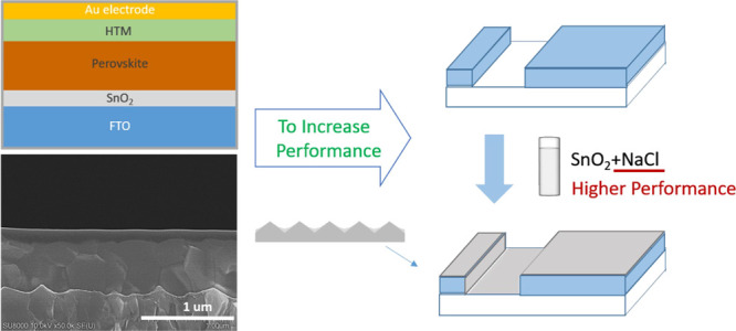
The structure of perovskite solar cells using the 25 mM NaCl-doped SnO2 composite as the ETL is illustrated in Figure 1, and the scanning electron microscopy (SEM) cross-section images of the perovskite solar cells using NaCl-doped SnO2 and undoped SnO2 device are displayed in Figure 2. The thickness of each layer could be obtained through the above cross-section image, where the Spiro-MeOTAD layer (HTL) was ca. 140 nm, the perovskite layer was about 560 nm, the NaCl-doped SnO2 layer (ETL) was approximately 40 nm, and undoped SnO2 ETL was approximately 30 nm. The PCE, open-circuit voltage, short-circuit current density, and FF at various NaCl concentrations are shown in Figure 3. The FF increases after the introduction of NaCl up to a concentration of 25 mM. The PCE reaches the highest value of 20.7% with the NaCl concentration of 25 mM, apparently improving the device performance compared to control devices (PCE 18.9% with only the SnO2 ETL). The hysteresis could also be improved by NaCl treatment, and the hysteresis reaches the lowest value of 0.5% with the NaCl concentration of 25 mM (Figure S3).
Figure 1.
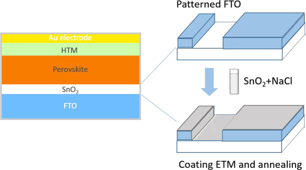
Fabrication process of the NaCl-doped SnO2 composite ETL and the device structure of planar perovskite solar cells.
Figure 2.

SEM cross-section image of a perovskite solar cell with (a and b) 25 mM NaCl-doped SnO2; (c and d) undoped SnO2 ETL.
Figure 3.

PCE, FF, Voc, and Jsc of SnO2 ETL perovskite solar cells at various concentrations of NaCl.
The PCE of best cells fabricated by NaCl-doped SnO2 and SnO2 is presented in Figure 4 and Table 1. The perovskite solar cells with NaCl-doped SnO2 and with only SnO2 show power conversion efficiencies of 20.7 and 18.9%, respectively, under forward scan, and 20.1 and 18.5% under reverse scan. The improved PCE in the NaCl-doped SnO2 perovskite solar cell is mainly caused by the obvious enhancement in FF. The Jsc value is slightly increased owing to the higher charge extraction efficiency in the NaCl-doped SnO2 perovskite solar cells, as indicated by the slightly better external quantum efficiency (EQE) values (Figure 5).
Figure 4.

I–V curves of the NaCl-doped SnO2 and SnO2 ETL best cells under forward scan.
Table 1. I–V Performance of Best Cells Using SnO2- and NaCl-Doped SnO2 Composite ETLs.
| ETL | direction | Jsc (mA/cm2) | Voc (V) | FF | PCE (%) |
|---|---|---|---|---|---|
| SnO2 | forward | 25.292 | 1.044 | 0.715 | 18.89 |
| reverse | 25.047 | 1.042 | 0.709 | 18.50 | |
| 25 mM NaCl-doped SnO2 | forward | 25.527 | 1.069 | 0.758 | 20.68 |
| reverse | 25.242 | 1.067 | 0.746 | 20.09 |
Figure 5.
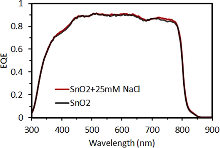
EQE spectra of the best cells based on NaCl-doped SnO2 and SnO2 ETLs.
To realize the efficiency improvement caused by the doping of NaCl into the SnO2 ETL, this study indicated the properties of SnO2 colloid solution, ETL, and perovskite layer with and without NaCl. N-x was employed to indicate different concentrations of NaCl physically blended in SnO2 colloid solution, where x represents the doping concentration in mM. Dynamic light scattering (DLS) analysis and zeta potential were implemented to investigate the agglomeration of SnO2 particles in water solution when different concentrations of NaCl were doped. Figure 6 shows the number distribution and the cumulative proportion of different sizes of SnO2 particles in water solution. The corresponding average particle size of SnO2 particles is summarized in Table 2. The number distribution of SnO2 particles was rarely changed regardless of NaCl concentrations as shown in Figure 6. The average particle size is less than 10 nm when NaCl was introduced up to a concentration of 50 mM. However, a conspicuous shift in average particle size was observed, especially in the N-100 condition. The zeta potential is a physical quantity that quantitatively describes the degree of electrostatic repulsion between the charged particles, and a colloid dispersion with a high zeta potential can resist the aggregation of the nanoparticles and remain stable.38 The zeta potential is −57.7 mV for the reference solution, but it reduces to −26.3 mV after adding 100 mM NaCl (Table S1). The decreased zeta potential and increased average particle size suggest the occurrence of colloid coagulation. The SnO2 colloid coagulation can be explained by the ion property of NaCl. Adding NaCl, a strong electrolyte, shields the negative charges of the colloidal SnO2 nanoparticles and causes them to clump together to form larger aggregates.39 Those NaCl would interact with KOH serving as the dispersion agent in SnO2 colloidal solution,40 reducing repulsive forces between each SnO2 particles. Therefore, the agglomeration of SnO2 particles happened because of the incorporation of NaCl.
Figure 6.

Number distribution and cumulative proportion of different sizes of SnO2 particles in (a) N-0, (b) N-25, (c) N-50, and (d) N-100 colloid solutions.
Table 2. Average Size of SnO2 Particles in Different Concentrations of NaCl Water Solution.
| ETL | N-0 | N-25 | N-50 | N-100 |
|---|---|---|---|---|
| average size (nm) | 2.5 ± 0.7 | 2.8 ± 1.5 | 8.5 ± 2.4 | 51.9 ± 14.6 |
To verify that NaCl was indeed incorporated in the as-spun SnO2 layer and to study the influence of NaCl to SnO2 film, SEM and energy dispersive X-ray spectroscopy (EDS) were applied to investigate the SnO2 film quality and the existence of NaCl. The polyhedral crystals in the SEM image refer to the fluorine tin oxide (FTO) substrate (Figure 7). Annealing of the as-spun SnO2 film will cause the agglomeration of SnO2 particles.41 The presence of NaCl prevents SnO2 particles from aggregating while annealing at 60 °C, resulting in a well-distributed ETL. The increasing signal quantity of Cl– element mapping from EDS directly proved that NaCl was successfully doped into the SnO2 layer under different concentrations (Figure 7b,d,f,h). Notice that the Cl element signal also emerged in N-0, which presumably came from the glass substrate itself.
Figure 7.

SEM images and EDS Cl– element mapping of (a, b) N-0; (c, d) N-25; (e, f) N-50, and (g, h) N-100 SnO2 film.
Transmittance of FTO/NaCl-doped SnO2 is shown in Figure 8. Doping NaCl into SnO2 had scarcely any influence on the transmittance, which is favorable since light being absorbed by perovskite layer needs to penetrate through FTO glass and ETL as the prerequisite. A lower transmittance means a lower amount of light harvested by perovskite, causing a drastic decrease in device performance, especially in short-circuit current density (Jsc). The SnO2 layer is very thin and the amount of NaCl actually deposited on it is too less to shade the incoming light, resulting in the unchanged transmittance consequently.
Figure 8.

Transmittance of FTO/NaCl-SnO2.
Despite the consistency of transmittance, the conductivity had a conspicuous change after NaCl doping. The electric property of NaCl-doped SnO2 films could be determined through the current–voltage characteristics (I–V curves) of the FTO/NaCl-doped SnO2/Au structure and the result is shown in Figure 9. According to the equation: I = σ0Ad–1V, where I is the current, σ0 is the conductivity of the films, A represents the area of the film, d is the thickness, and V is the applied voltage.42 The calculated conductivities are listed in Table 3. The conductivity of SnO2 was enhanced and reached its maximum with an approximately 1000 times promotion when 50 mM NaCl was doped in SnO2. Different additives into SnO2 will ameliorate the conductivity of the SnO2 film in various ways, such as boosting the disaggregation of SnO2 colloid to form a compact layer,43 elevating free electron density in the conduction band of SnO2 via providing free electrons from the additives,44 and reducing defects in ETL.45 The enhancement of conductivity by adding NaCl in SnO2 here presumably resulted from the much denser SnO2 layer, originating from the well dispersed SnO2 particles and NaCl filling vacancies between SnO2 particles. A dense SnO2 layer could provide more pathways for electron transportation. The lower amount of vacancies by the passivation of NaCl in the SnO2 layer would also reduce the probability of electron scattering, which is destructive for charge transfer. However, the overdose of NaCl addition would pull down the effective conductivity of the as-prepared SnO2 film contrarily (in N-100 case). This could be explained by the fact that NaCl is not a well electrically conductive material in the solid state, and charge scattering originating from NaCl particles may not be ignored anymore.
Figure 9.
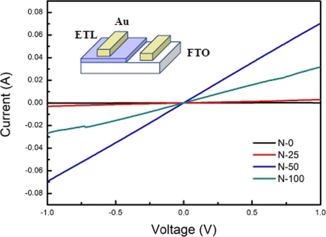
I–V curves of the FTO/NaCl-doped SnO2/Au planar structure with different NaCl doping concentrations. The inset shows the schematic device structure for conductivity measurement.
Table 3. Conductivities of FTO/NaCl-Doped SnO2/Au with Different NaCl Doping Concentrations.
| ETL | N-0 | N-25 | N-50 | N-100 |
|---|---|---|---|---|
| conductivity (S/cm) | 2.10 × 10⁻⁸ | 5.92 × 10⁻⁷ | 1.36 × 10⁻⁵ | 5.19 × 10⁻⁶ |
The effects of various NaCl concentrations on the surface morphology and crystallinity of the perovskite films were evaluated by using X-ray diffraction (XRD), atomic force microscopy (AFM) and SEM (Figures S1 and S2). Considering that NaCl was just physically blended with SnO2 particles in water solution, it was certain that some NaCl would exist on the surface of the as-spun NaCl-doped SnO2 film, affecting the following crystal growth of perovskite. Figure 10 shows the XRD pattern of FTO/NaCl-doped SnO2/perovskite devices. The asterisk marked peaks stood for the tetragonal tin oxide from FTO and as-spun SnO2. The hashtag labeled peaks represented lead iodide (001). Peaks with labeled lattice planes came from the perovskite crystal. The perovskite material used here as a light harvester was cesium doped formamidinium lead iodide with chemical formula HC(NH2)2PbI3, abbreviated as FAPbI3. The FAPbI3 perovskite crystal can be divided into two phases, which are alpha phase and delta phase.46,47 α-FAPbI3 belongs to the cubic lattice system with black color and has the desired properties for photovoltaics, while δ-FAPbI3 is a hexagonal lattice possessing yellow color and is unsuitable for light harvesting. The as-synthesized α-FAPbI3 will easily change to δ-FAPbI3 at room temperature, diminishing device performance, however. Fortunately, this problem could be solved by cesium doping. Cs+ cations can fractionally substitute FA+ cations at the A site of the perovskite crystal, forming CsxFA1–xPbI3, where x is the fraction of doped cesium. The partial substitution of FA+ ions (1.9–2.2 Å) by much smaller Cs+ ions (1.81 Å) will significantly improve its stability and the photovoltaic behavior.46−48 As we could see in Figure 10, the peak of δ-FAPbI3 located at 11.78°46,47,49 was not found and the CsPbI3 peak positioned at 9.8° was not observed either, indicating that cesium atoms were successfully doped into α-FAPbI3 and pure CsxFA1–xPbI3 was produced.
Figure 10.

XRD patterns of perovskite crystals on FTO/NaCl-doped SnO2 substrates.
The magnified XRD pattern from 12° to 14.5° is further depicted in Figure 11 to investigate the relation between NaCl and perovskite crystal growth. The peak at 12.67° was from nonreacted PbI2 (001), while the peak of the CsxFA1–xPbI3 (001) plane was located at 13.98°. The measured peak was fitted by a Gaussian function and the full width at half maximum (FWHM) was calculated subsequently. The determined FWHM was then deployed into the Scherrer equation to obtain the crystal grain size. The Scherrer equation is a practical way to determine the crystal grain size in a specific direction, which can be written as Dhkl = 0.9λ/βhklcos(θ). Dhkl is the grain size in the (hkl) direction in nm, λ is the wavelength of incident X-ray, which is 0.15 nm for Cu Kα. θ is the Bragg angle of the crystal in degree, and βhkl is the calculated FWHM in radian. The resulting FWHMs and calculated grain sizes of PbI2 (001) and CsxFA1–xPbI3 (001) are summarized in Table 4. Both PbI2 and CsxFA1–xPbI3 crystals became larger along with the increasing NaCl doping amount in the SnO2 film. The possible mechanism is some portion of NaCl blended with SnO2 would locate on the surface of the as-spun SnO2 film, being able to dissolve into the perovskite precursor solution during the following spinning process. The dissolved NaCl was considered to interact with PbI2 in the solvent. PbI2 is a quasi-two-dimensional semiconductor. A layer of Pb atoms is sandwiched between two layers of I atoms. This I-Pb-I structure is then repeated to form the basic configuration of PbI2. These I-Pb-I repeating units are combined through van der Waals interactions, which are relatively weak in contrast to the covalent interactions in the intralayers.50 NaCl dissolved in perovskite solution could insert into I-Pb-I layers, producing NaCl–PbI2 intermediates.51 These stable intermediates would retard the reaction between FAI and PbI2 and the amount of precipitated perovskite crystal, which was referred to as nuclei, from the FAI-DMSO-PbI2 precursor solution before annealing would drop. The less the existence of nuclei, the larger the final crystal dimension. Hence, the increasing perovskite crystal size accompanied by the more NaCl doping concentrations in SnO2 was due to the increased formation of the NaCl–PbI2 intermediate.
Figure 11.
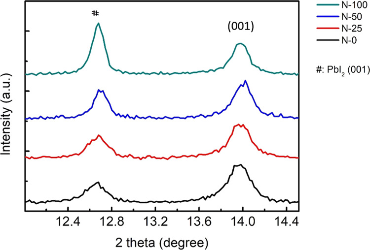
Magnified XRD patterns of perovskite crystals on FTO/NaCl-doped SnO2 substrates.
Table 4. FWHM and the Corresponding Crystal Size of PbI2 (001) and CsxFA1–xPbI3 (001) on Different FTO/NaCl-Doped SnO2 Substrates.
| ETL | FWHM (radian) | crystal size (nm) | FWHM (radian) | crystal size (nm) |
|---|---|---|---|---|
| PbI2 | PbI2 | perovskite | perovskite | |
| N-0 | 0.00366 | 39 | 0.00401 | 35 |
| N-25 | 0.00349 | 40 | 0.00366 | 40 |
| N-50 | 0.00262 | 56 | 0.00332 | 43 |
| N-100 | 0.00244 | 60 | 0.00297 | 47 |
Figure 12 shows the SEM images of the perovskite layer on different NaCl-doped SnO2 substrates. The polygon shapes of 500–1000 nm in diameter were recognized as the perovskite crystal and were quite similar to the research reported by Prathapani et al.49 A large perovskite crystal size is preferred for two reasons: grain boundaries will serve as charge recombination centers. A large crystal size can reduce the amount of grain boundary per volume, so the problematic charge recombination can be suppressed and Voc and FF of the solar cell can be augmented.10,52 In terms of the charge transfer process, a large perovskite crystal is more likely to provide a long-range travel distance for photoinduced charges, which can also promote the device performance.53 The large crystal size here was superb for high efficiency perovskite solar cells. In Figure 12a, perovskite formed on the SnO2 ETL without NaCl modification showed apparently obvious cracks between crystals. By contrast, perovskite on N-25 ETL (Figure 12b) showed an exceedingly dense layer. For the perovskite layer on N-50 and N-100 ETL (Figure 12c,d), a rough surface was produced. This rough surface would raise the charge recombination centers, which was a disadvantage for cell performance. However, the perovskite crystal on 25 mM NaCl-doped SnO2 became more homogeneous than undoped SnO2. This indicated that 25 mM NaCl doping treatment could optimize the perovskite morphology so as to obtain full-coverage and a uniform perovskite film compared to undoped SnO2, which is beneficial for the light absorption and charge transport. For high-performance solar cells, a homogeneous perovskite film with well surface coverage is highly desirable because cracks or pinholes could cause a direct contact between the ETL and the HTL, resulting in a shunting pathway. In this respect, the compact film produced from the 25 mM NaCl-doped SnO2 ETL led to a better high-performance perovskite solar cell.
Figure 12.

SEM perovskite layer images of (a) N-0; (b) N-25; (c) N-50; and (d) N-100 films.
The analysis of photoluminescence decay in time-resolved photoluminescence (TRPL) spectroscopy was therefore an effective way to determine the recombination kinetics of NaCl-doped SnO2/CsFAPbI3 perovskite (Figure 13). The perovskite layer was illuminated by a laser pulse from the perovskite side with an excitation wavelength of 532 nm and photogenerated electron hole pairs emerged in the perovskite layer. The photogenerated electrons then diminished through different processes. Hence, the existing electrons being able to recombine with electric holes in the perovskite layer, which could generate light detected by the TRPL equipment, reduced. The PL decay curve was then fitted with a biexponential function, consisting of two terms: a quick decay (τ1) and a slow decay (τ2), respectively (Table 5).32 The quick decay (τ1) is attributed to the charge extraction by the ETL, while the slow decay (τ2) to the recombination process inside the perovskite film.32 The decrease of quick decay lifetime τ1 from 10.39 ns (SnO2) to 8.91 ns (25 mM NaCl-doped SnO2) and the increase of the proportion of τ1 from 0.57 (SnO2) to 0.59 (25 mM NaCl-doped SnO2) indicate electron transfer from perovskite to the ETL more quickly with 25 mM of NaCl addition. The slightly slow decay lifetime τ2 increase from 51.57 to 55.33 ns for the perovskite film on the 25 mM NaCl-doped SnO2 ETL indicates a slightly lower nonradiative recombination rate inside the perovskite film. The reduced recombination could be attributed to the passivation of perovskite grain by Na+ and Cl– ions. However, there is no large difference on the PL lifetime between pure SnO2 and 25 mM NaCl-doped SnO2.
Figure 13.

TRPL spectra of FTO/NaCl-doped SnO2/perovskite with different concentrations of NaCl-modified SnO2 as substrates.
Table 5. Fast and Slow Components for the PL Decay and Their Corresponding Proportions.
| ETL | N-0 | N-25 | N-50 | N-100 |
|---|---|---|---|---|
| A1 | 0.57 | 0.59 | 0.74 | 0.48 |
| τ1 (ns) | 10.39 | 8.91 | 6.37 | 11.26 |
| A2 | 0.43 | 0.41 | 0.26 | 0.52 |
| τ2 (ns) | 51.57 | 55.33 | 44.33 | 65.29 |
3. Conclusions
In summary, a sodium chloride (NaCl) modification had demonstrated that the NaCl-doped SnO2 composite ETL will effectively improve the planar perovskite solar cell performance. The NaCl of the composite ETL contributes to interface passivation and reduces the nonradiative recombination in perovskite photovoltaics. The NaCl modification to SnO2 had reached a great success in increasing the conductivity of the SnO2 ETL and reducing the defect density in the perovskite layer, hence promoting the electron transfer efficiency from the perovskite layer to ETL and the PCE of the SnO2-based planar perovskite solar cell. The NaCl-doped SnO2 composite ETL perovskite solar cells have demonstrated a best PCE performance of 20.7% with effective improvement in the FF. This facile sodium chloride modification strategy to the tin oxide ETL could provide an uncomplicated approach for fabricating perovskite photovoltaics with significant performance improvements.
4. Experimental Section
4.1. Materials and Device Fabrication
The NaCl-doped SnO2 composite ETL was fabricated by mixing NaCl in the SnO2 colloidal solution and then deposited on a FTO conductive glass substrate. The perovskite material with a composition of Cs0.1FA0.9PbI3 was prepared by applying the antisolvent deposition method.4
The patterned FTO glass (10 Ω/□, Nippon Sheet Glass Co., Ltd., Japan) was cleaned with acetone and ethanol, respectively, and dried with N2 gas flow. UV-Ozone (ASM1101N; Asumi Giken Co., Ltd., Japan) cleaning is then applied for 15 min to remove the organic particles and to enhance the wettability of the patterned FTO surface. The ETL precursor solution is prepared in advance. SnO2 ETL solution (tin(IV) oxide, 15% in H2O colloidal dispersion liquid; Alfa Aesar Co., Ltd., USA) contains 2.5 wt % of SnO2 colloid water solution with 0/25/50/100 mM NaCl (Sodium Chloride >99.5%; Sigma Aldrich Co., Ltd., USA) doping concentrations. The prepared ETL solution (85 μL) is then spin coated (MS-B100; Mikasa Co., Ltd., Japan) on the patterned FTO substrate at 4000 rpm for 30 s. The as-spun ETL is subsequently annealed at 60 °C for 30 min and cooled to room temperature for the following procedure.
CsI (0.14 M) (cesium iodide >99.0%; TCI Co., Ltd., Japan), FAI (1.26 M) (formamidine hydroiodide > 98%; TCI Co., Ltd., Japan), PbI2 (1.4 M) (Lead(II) iodide 99.9%; TCI Co., Ltd., Japan) are dissolved in a 4:1 (v:v) mixture of N,N-dimethylformamide and dimethyl sulfoxide (super-dehydrated; Fujifilm Co., Ltd., Japan) to form perovskite precursor solution. The precursor solution is rested for another 30 min to make sure the solutes are completely dissolved. The as-prepared perovskite precursor solution (100 μL) is spin coated onto the ETL through a process (1000 rpm for 10 s then 4000 rpm for 30 s) with dripping of chlorobenzene (600 μL) as the antisolvent at the last 10 s. The deposited perovskite layer is then immediately transferred to the hot plate to anneal at 155 °C for exact 15 min.
The HTL precursor solution needs to be prepared in a specific sequence to avoid the presence of undissolved lithium. 1 mL of Spiro-MeOTAD (SHT-263 Solarpur; Sigma Aldrich Co., Ltd., USA) solution containing 72.3 mg of Spiro-MeOTAD powder in 1 mL of chlorobenzene (Chlorobenzene anhydrous 99.8%; Sigma Aldrich Co., Ltd., USA) is mixed with 17.5 μL of Li-TFSI solution (520 mg of Li-TFSI in 1 mL of acetonitrile) (Li-TFSI; bis(trifluoromethane) sulfonamide lithium salt 99.95%; Sigma Aldrich Co., Ltd., USA) (acetonitrile, super-dehydrated; Fujifilm Co., Ltd., Japan). This intermediate solution is then added with 28.75 μL of 4-tert-butylpyridine (>96%; TCI Co., Ltd., Japan). The HTL solution is spin coated on a perovskite layer at 4000 rpm for 30 s and then an 80 nm-thick gold electrode is deposited on the HTL using a thermal coater. Oxidization of HTL is implemented in the dry room with humidity under 500 ppm one day for aging.
4.2. Device Characterization
The photocurrent–density–voltage (J–V) characteristics of the cells were measured under AM 1.5 G illumination (100 mW cm–2) with a 450 W xenon light source (YSS-80A; Yamashita Denso Co., Ltd., Japan). The light source was calibrated using a Si photodiode (BS-520, Bunkoukeiki Co., Ltd., Japan) with an optical filter (KG5, Bunkoukeiki Co., Ltd., Japan). The scanning speed was fixed at 50 mVs–1. Spectra of the incident-photon-to-electron conversion efficiency (IPCE) of the cells were measured using a solar simulator (CEP-2000MLQ, Bunkoukeiki Co., Ltd., Japan) in the direct current mode without bias. The excitation light intensity was calibrated using a Si photodiode. A metal-aperture mask was used to define an active area of 0.18 cm2 during the J–V and IPCE measurements. Transmittance of the NaCl-doped SnO2 film coated on the FTO glass was obtained using an ultraviolet–visible (UV–vis) spectrometer (UV3600, Shimadzu, Japan) equipped with an integrating sphere. The surface morphology and thickness of each film were analyzed with a field-emission SEM (SU8000, Hitachi, Japan). XRD patterns of the SnO2 and perovskite films were measured using a X-ray diffractometer (D8 Discover, Bruker, Germany) with Cu Kα radiation (λ = 0.15406 nm). DLS (Delsa NanoC, DLS, Beckman Coulter, USA) was implemented to measure the particle size of the SnO2 colloid solution when different amounts of NaCl was doped, since the attachment of NaCl on SnO2 particles may affect its dispersion in the solvent. TRPL was conducted using a microphotoluminescence system. TRPL spectra can demonstrate the exact electron loss mechanism through the biexponential fitting of the measured TRPL decay spectra.
Acknowledgments
This work was supported by the New Energy and Industrial Technology Development Organization (NEDO) of Japan and National Yang Ming Chiao Tung University (NYCU) of Taiwan.
Supporting Information Available
The Supporting Information is available free of charge at https://pubs.acs.org/doi/10.1021/acsomega.1c01286.
Surface roughness of the ETL; SEM cross-section images and AFM top-view images of the SnO2 ETL with different doping concentrations of NaCl; hysteresis index of various NaCl doping concentrations in the SnO2 ETL perovskite solar cell device; zeta potential value of SnO2 colloidal solution with different NaCl doping concentrations (PDF)
The authors declare no competing financial interest.
Notes
The authors declare that they have no known competing financial interests or personal relationships that could have appeared to influence the work reported in this paper.
Supplementary Material
References
- Gao F.; Zhao Y.; Zhang X.; You J. Recent Progresses on Defect Passivation toward Efficient Perovskite Solar Cells. Adv. Energy Mater. 2020, 10, 1902650 10.1002/aenm.201902650. [DOI] [Google Scholar]
- Kojima A.; Teshima K.; Shirai Y.; Miyasaka T. Organometal Halide Perovskites as Visible-Light Sensitizers for Photovoltaic Cells. J. Am. Chem. Soc. 2009, 131, 6050–6051. 10.1021/ja809598r. [DOI] [PubMed] [Google Scholar]
- Kim H.-S.; Lee C.-R.; Im J.-H.; Lee K.-B.; Moehl T.; Marchioro A.; Moon S.-J.; Humphry-Baker R.; Yum J.-H.; Moser J. E.; Grätzel M.; Park N.-G. Lead Iodide Perovskite Sensitized All-Solid-State Submicron Thin Film Mesoscopic Solar Cell with Efficiency Exceeding 9%. Sci. Rep. 2012, 2, 591. 10.1038/srep00591. [DOI] [PMC free article] [PubMed] [Google Scholar]
- Tang Z.; Bessho T.; Awai F.; Kinoshita T.; Maitani M. M.; Jono R.; Murakami T. N.; Wang H.; Kubo T.; Uchida S.; Segawa H. Hysteresis-Free Perovskite Solar Cells Made of Potassium-Doped Organometal Halide Perovskite. Sci. Rep. 2017, 7, 12183. 10.1038/s41598-017-12436-x. [DOI] [PMC free article] [PubMed] [Google Scholar]
- Wang L.; Zhou H.; Hu J.; Huang B.; Sun M.; Dong B.; Zheng G.; Huang Y.; Chen Y.; Li L.; Xu Z.; Li N.; Liu Z.; Chen Q.; Sun L.-D.; Yan C.-H. A Eu3+-Eu2+ Ion Redox Shuttle Imparts Operational Durability to Pb-I Perovskite Solar Cells. Science 2019, 363, 265–270. 10.1126/science.aau5701. [DOI] [PubMed] [Google Scholar]
- Jiang Q.; Zhao Y.; Zhang X.; Yang X.; Chen Y.; Chu Z.; Ye Q.; Li X.; Yin Z.; You J. Surface Passivation of Perovskite Film for Efficient Solar Cells. Nat. Photonics 2019, 13, 460–466. 10.1038/s41566-019-0398-2. [DOI] [Google Scholar]
- Lee M. M.; Teuscher J.; Miyasaka T.; Murakami T. N.; Snaith H. J. Efficient Hybrid Solar Cells Based on Meso-Superstructured Organometal Halide Perovskites. Science 2012, 338, 643–647. 10.1126/science.1228604. [DOI] [PubMed] [Google Scholar]
- Jiang Q.; Zhang L.; Wang H.; Yang X.; Meng J.; Liu H.; Yin Z.; Wu J.; Zhang X.; You J. Enhanced Electron Extraction Using SnO2 for High-Efficiency Planar-Structure HC(NH2)2PbI3-Based Perovskite Solar Cells. Nat. Energy 2017, 2, 16177. 10.1038/nenergy.2016.177. [DOI] [Google Scholar]
- Eperon G. E.; Stranks S. D.; Menelaou C.; Johnston M. B.; Herz L. M.; Snaith H. J. Formamidinium Lead Trihalide: a Broadly Tunable Perovskite for Efficient Planar Heterojunction Solar Cells. Energy Environ. Sci. 2014, 7, 982. 10.1039/C3EE43822H. [DOI] [Google Scholar]
- Shi D.; Adinolfi V.; Comin R.; Yuan M.; Alarousu E.; Buin A.; Chen Y.; Hoogland S.; Rothenberger A.; Katsiev K.; Losovyj Y.; Zhang X.; Dowben P. A.; Mohammed O. F.; Sargent E. H.; Bakr O. M. Low Trap-State Density and Long Carrier Diffusion in Organolead Trihalide Perovskite Single Crystals. Science 2015, 347, 519–522. 10.1126/science.aaa2725. [DOI] [PubMed] [Google Scholar]
- Wang Y.; Bai S.; Cheng L.; Wang N.; Wang J.; Gao F.; Huang W. High-Efficiency Flexible Solar Cells Based on Organometal Halide Perovskites. Adv. Mater. 2015, 28, 4532–4540. 10.1002/adma.201504260. [DOI] [PubMed] [Google Scholar]
- Dong Q.; Fang Y.; Shao Y.; Mulligan P.; Qiu J.; Cao L.; Huang J. Electron-Hole Diffusion Lengths > 175 Μm in Solution-Grown CH3NH3PbI3 single Crystals. Science 2015, 347, 967–970. 10.1126/science.aaa5760. [DOI] [PubMed] [Google Scholar]
- Murakami T. N.; Miyadera T.; Funaki T.; Cojocaru L.; Kazaoui S.; Chikamatsu M.; Segawa H. Adjustment of Conduction Band Edge of Compact TiO2 Layer in Perovskite Solar Cells Through TiCl4 Treatment. ACS Appl. Mater. Interfaces 2017, 9, 36708–36714. 10.1021/acsami.7b07496. [DOI] [PubMed] [Google Scholar]
- Jeon N. J.; Noh J. H.; Yang W. S.; Kim Y. C.; Ryu S.; Seo J.; Seok S. I. Compositional Engineering of Perovskite Materials for High-Performance Solar Cells. Nature 2015, 517, 476–480. 10.1038/nature14133. [DOI] [PubMed] [Google Scholar]
- Chen W.; Wu Y.; Yue Y.; Liu J.; Zhang W.; Yang X.; Chen H.; Bi E.; Ashraful I.; Gratzel M.; Han L. Efficient and Stable Large-Area Perovskite Solar Cells with Inorganic Charge Extraction Layers. Science 2015, 350, 944–948. 10.1126/science.aad1015. [DOI] [PubMed] [Google Scholar]
- Zhou H.; Chen Q.; Li G.; Luo S.; Song T.; Duan H. S.; Hong Z.; You J.; Liu Y.; Yang Y. Interface Engineering of Highly Efficient Perovskite Solar Cells. Science 2014, 345, 542–546. 10.1126/science.1254050. [DOI] [PubMed] [Google Scholar]
- Wu Y.; Islam A.; Yang X.; Qin C.; Liu J.; Zhang K.; Peng W.; Han L. Retarding the Crystallization of PbI2 for Highly Reproducible Planar-Structured Perovskite Solar Cells via Sequential Deposition. Energy Environ. Sci. 2014, 7, 2934–2938. 10.1039/C4EE01624F. [DOI] [Google Scholar]
- Bi D.; Yi C.; Luo J.; Décoppet J.-D.; Zhang F.; Zakeeruddin S. M.; Li X.; Hagfeldt A.; Grätzel M. Polymer-Templated Nucleation and Crystal Growth of Perovskite Films for Solar Cells with Efficiency Greater than 21%. Nat. Energy 2016, 1, 16142. 10.1038/nenergy.2016.142. [DOI] [Google Scholar]
- Davies C. L.; Filip M. R.; Patel J. B.; Crothers T. W.; Verdi C.; Wright A. D.; Milot R. L.; Giustino F.; Johnston M. B.; Herz L. M. Bimolecular Recombination in Methylammonium Lead Triiodide Perovskite Is an Inverse Absorption Process. Nat. Commun. 2018, 9, 293. 10.1038/s41467-017-02670-2. [DOI] [PMC free article] [PubMed] [Google Scholar]
- Stolterfoht M.; Wolff C. M.; Márquez J. A.; Zhang S.; Hages C. J.; Rothhardt D.; Albrecht S.; Burn P. L.; Meredith P.; Unold T.; Neher D. Visualization and Suppression of Interfacial Recombination for High-Efficiency Large-Area Pin Perovskite Solar Cells. Nat. Energy 2018, 3, 847–854. 10.1038/s41560-018-0219-8. [DOI] [Google Scholar]
- Zheng X.; Chen B.; Dai J.; Fang Y.; Bai Y.; Lin Y.; Wei H.; Zeng X. C.; Huang J. Defect Passivation in Hybrid Perovskite Solar Cells Using Quaternary Ammonium Halide Anions and Cations. Nat. Energy 2017, 2, 17102. 10.1038/nenergy.2017.102. [DOI] [Google Scholar]
- Guo P.; Yang X.; Ye Q.; Zhang J.; Wang H.; Yu H.; Zhao W.; Liu C.; Yang H.; Wang H. Anti-Colloidal-Solutions: Laser-Generated Nanocrystals in Perovskite: Universal Embedding of Ligand-Free and Sub-10nm Nanocrystals in Solution-Processed Metal Halide Perovskite Films for Effectively Modulated Optoelectronic Performance. Adv. Energy Mater. 2019, 9, 1970134 10.1002/aenm.201970134. [DOI] [Google Scholar]
- Aydin E.; Bastiani M.; Wolf S. Defect and Contact Passivation for Perovskite Solar Cells. Adv. Mater. 2019, 31, 1900428 10.1002/adma.201900428. [DOI] [PubMed] [Google Scholar]
- Tan H.; Jain A.; Voznyy O.; Lan X.; Arquer F. P. G. D.; Fan J. Z.; Quintero-Bermudez R.; Yuan M.; Zhang B.; Zhao Y.; Fan F.; Li P.; Quan L. N.; Zhao Y.; Lu Z.-H.; Yang Z.; Hoogland S.; Sargent E. H. Efficient and Stable Solution-Processed Planar Perovskite Solar Cells via Contact Passivation. Science 2017, 355, 722–726. 10.1126/science.aai9081. [DOI] [PubMed] [Google Scholar]
- Jiang Q.; Chu Z.; Wang P.; Yang X.; Liu H.; Wang Y.; Yin Z.; Wu J.; Zhang X.; You J. Planar-Structure Perovskite Solar Cells with Efficiency beyond 21%. Adv. Mater. 2017, 29, 1703852 10.1002/adma.201703852. [DOI] [PubMed] [Google Scholar]
- Wang F.; Geng W.; Zhou Y.; Fang H.-H.; Tong C.-J.; Loi M. A.; Liu L.-M.; Zhao N. Phenylalkylamine Passivation of Organolead Halide Perovskites Enabling High-Efficiency and Air-Stable Photovoltaic Cells. Adv. Mater. 2016, 28, 9986–9992. 10.1002/adma.201603062. [DOI] [PubMed] [Google Scholar]
- Noel N. K.; Abate A.; Stranks S. D.; Parrott E. S.; Burlakov V. M.; Goriely A.; Snaith H. J. Enhanced Photoluminescence and Solar Cell Performance via Lewis Base Passivation of Organic–Inorganic Lead Halide Perovskites. ACS Nano 2014, 8, 9815–9821. 10.1021/nn5036476. [DOI] [PubMed] [Google Scholar]
- Niu T.; Lu J.; Jia X.; Xu Z.; Tang M.-C.; Barrit D.; Yuan N.; Ding J.; Zhang X.; Fan Y.; Luo T.; Zhang Y.; Smilgies D. M.; Liu Z.; Amassian A.; Jin S.; Zhao K.; Liu S. Interfacial Engineering at the 2D/3D Heterojunction for High-Performance Perovskite Solar Cells. Nano Lett. 2019, 19, 7181–7190. 10.1021/acs.nanolett.9b02781. [DOI] [PubMed] [Google Scholar]
- Niu T.; Lu J.; Tang M.-C.; Barrit D.; Smilgies D.-M.; Yang Z.; Li J.; Fan Y.; Luo T.; Mcculloch I.; Amassian A.; Liu S. F.; Zhao K. High Performance Ambient-Air-Stable FAPbI3 Perovskite Solar Cells with Molecule-Passivated Ruddlesden–Popper/3D Heterostructured Film. Energy Environ. Sci. 2018, 11, 3358–3366. 10.1039/C8EE02542H. [DOI] [Google Scholar]
- Yoo J. J.; Wieghold S.; Sponseller M. C.; Chua M. R.; Bertram S. N.; Hartono N. T. P.; Tresback J. S.; Hansen E. C.; Correa-Baena J.-P.; Bulović V.; Buonassisi T.; Shin S. S.; Bawendi M. G. An Interface Stabilized Perovskite Solar Cell with High Stabilized Efficiency and Low Voltage Loss. Energy Environ. Sci. 2019, 12, 2192–2199. 10.1039/C9EE00751B. [DOI] [Google Scholar]
- Wang S.; Sakurai T.; Wen W.; Qi Y. Energy Level Alignment at Interfaces in Metal Halide Perovskite Solar Cells. Adv. Mater. Interfaces 2020, 7, 2000423. 10.1002/admi.201800260. [DOI] [Google Scholar]
- Li Z.; Wang L.; Liu R.; Fan Y.; Meng H.; Shao Z.; Cui G.; Pang S. Spontaneous Interface Ion Exchange: Passivating Surface Defects of Perovskite Solar Cells with Enhanced Photovoltage. Adv. Energy Mater. 2019, 9, 1902142 10.1002/aenm.201902142. [DOI] [Google Scholar]
- Abdi-Jalebi M.; Andaji-Garmaroudi Z.; Cacovich S.; Stavrakas C.; Philippe B.; Richter J. M.; Alsari M.; Booker E. P.; Hutter E. M.; Pearson A. J.; Lilliu S.; Savenije T. J.; Rensmo H.; Divitini G.; Ducati C.; Friend R. H.; Stranks S. D. Maximizing and Stabilizing Luminescence from Halide Perovskites with Potassium Passivation. Nature 2018, 555, 497–501. 10.1038/nature25989. [DOI] [PubMed] [Google Scholar]
- Niu T.; Lu J.; Munir R.; Li J.; Barrit D.; Zhang X.; Hu H.; Yang Z.; Amassian A.; Zhao K.; Liu S. F. Stable High-Performance Perovskite Solar Cells via Grain Boundary Passivation. Adv. Mater. 2018, 30, 1706576 10.1002/adma.201706576. [DOI] [PubMed] [Google Scholar]
- Son D.-Y.; Lee J.-W.; Choi Y. J.; Jang I.-H.; Lee S.; Yoo P. J.; Shin H.; Ahn N.; Choi M.; Kim D.; Park N.-G. Self-Formed Grain Boundary Healing Layer for Highly Efficient CH3NH3PbI3 Perovskite Solar Cells. Nat. Energy 2016, 1, 16081. 10.1038/nenergy.2016.81. [DOI] [Google Scholar]
- Bag S.; Durstock M. F. Large Perovskite Grain Growth in Low-Temperature Solution-Processed Planar p-i-n Solar Cells by Sodium Addition. ACS Appl. Mater. Interfaces 2016, 8, 5053–5057. 10.1021/acsami.5b11494. [DOI] [PubMed] [Google Scholar]
- Ma J.; Guo X.; Zhou L.; Lin Z.; Zhang C.; Yang Z.; Lu G.; Chang J.; Hao Y. Enhanced Planar Perovskite Solar Cell Performance via Contact Passivation of TiO2/Perovskite Interface with NaCl Doping Approach. ACS Appl. Energy Mater. 2018, 1, 3826–3834. 10.1021/acsaem.8b00602. [DOI] [Google Scholar]
- Sethi M.; Joung G.; Knecht M. R. Stability and Electrostatic Assembly of Au Nanorods for Use in Biological Assays. Langmuir 2009, 25, 317–325. 10.1021/la802096v. [DOI] [PubMed] [Google Scholar]
- Bhamore J.; Rawat K. A.; Basu H.; Singhal R. K.; Kailasa S. K. Influence of molecular assembly and NaCl concentration on gold nanoparticles for colorimetric detection of cysteine and glutathione. Sens. Actuators, B 2015, 212, 526–535. 10.1016/j.snb.2015.01.133. [DOI] [Google Scholar]
- Bu T.; Li J.; Zheng F.; Chen W.; Wen X.; Ku Z.; Peng Y.; Zhong J.; Cheng Y. B.; Huang F. Universal passivation strategy to slot-die printed SnO2 for hysteresis-free efficient flexible perovskite solar module. Nat. Commun. 2018, 9, 4609. 10.1038/s41467-018-07099-9. [DOI] [PMC free article] [PubMed] [Google Scholar]
- Ke W.; Zhao D.; Cimaroli A. J.; Grice C. R.; Qin P.; Liu Q.; Xiong L.; Yan Y.; Fang G. Effects of Annealing Temperature of Tin Oxide Electron Selective Layers on the Performance of Perovskite Solar Cells. J. Mater. Chem. A 2015, 3, 24163–24168. 10.1039/C5TA06574G. [DOI] [Google Scholar]
- Yang Z.; Xie J.; Arivazhagan V.; Xiao K.; Qiang Y.; Huang K.; Hu M.; Cui C.; Yu X.; Yang D. Efficient and Highly Light Stable Planar Perovskite Solar Cells with Graphene Quantum Dots Doped PCBM Electron Transport Layer. Nano Energy 2017, 40, 345–351. 10.1016/j.nanoen.2017.08.008. [DOI] [Google Scholar]
- Wei J.; Guo F.; Wang X.; Xu K.; Lei M.; Liang Y.; Zhao Y.; Xu D. SnO2-in-Polymer Matrix for High-Efficiency Perovskite Solar Cells with Improved Reproducibility and Stability. Adv. Mater. 2018, 30, 1805153. 10.1039/C7TA08040A. [DOI] [PubMed] [Google Scholar]
- Xie J.; Huang K.; Yu X.; Yang Z.; Xiao K.; Qiang Y.; Zhu X.; Xu L.; Wang P.; Cui C.; Yang D. Enhanced Electronic Properties of SnO2 via Electron Transfer from Graphene Quantum Dots for Efficient Perovskite Solar Cells. ACS Nano 2017, 11, 9176–9182. 10.1021/acsnano.7b04070. [DOI] [PubMed] [Google Scholar]
- Wang S.; Zhu Y.; Liu B.; Wang C.; Ma R. Introduction of Carbon Nanodots into SnO2 Electron Transport Layer for Efficient and UV Stable Planar Perovskite Solar Cells. J. Mater. Chem. A 2019, 7, 5353–5362. 10.1039/C8TA11651B. [DOI] [Google Scholar]
- Wang H.; Wu H.; Xian Y.; Niu G.; Yuan W.; Li H.; Yin H.; Liu P.; Long Y.; Li W.; Fan J. Controllable CsxFA1–xPbI3 Single-Crystal Morphology via Rationally Regulating the Diffusion and Collision of Micelles toward High-Performance Photon Detectors. ACS Appl. Mater. Interfaces 2019, 11, 13812–13821. 10.1021/acsami.9b02840. [DOI] [PubMed] [Google Scholar]
- Hou X.; Xu M.; Tong C.; Ji W.; Fu Z.; Wan Z.; Hao F.; Ming Y.; Liu S.; Hu Y.; Han H.; Rong Y.; Yao Y. High Performance Printable Perovskite Solar Cells Based on Cs0.1FA0.9PbI3 in Mesoporous Scaffolds. J. Power Sources 2019, 415, 105–111. 10.1016/j.jpowsour.2019.01.065. [DOI] [Google Scholar]
- Li Z.; Yang M.; Park J.-S.; Wei S.-H.; Berry J. J.; Zhu K. Stabilizing Perovskite Structures by Tuning Tolerance Factor: Formation of Formamidinium and Cesium Lead Iodide Solid-State Alloys. Chem. Mater. 2015, 28, 284–292. 10.1021/acs.chemmater.5b04107. [DOI] [Google Scholar]
- Prathapani S.; Choudhary D.; Mallick S.; Bhargava P.; Yella A. Experimental Evaluation of Room Temperature Crystallization and Phase Evolution of Hybrid Perovskite Materials. CrystEngComm 2017, 19, 3834–3843. 10.1039/C7CE00402H. [DOI] [Google Scholar]
- Beckmann P. A. A Review of Polytypism in Lead Iodide. Cryst. Res. Technol. 2010, 45, 455–460. 10.1002/crat.201000066. [DOI] [Google Scholar]
- Lee H.; Kim A.; Kwon H.-C.; Yang W.; Oh Y.; Lee D.; Moon J. Retarding Crystallization during Facile Single Coating of NaCl-Incorporated Precursor Solution for Efficient Large-Area Uniform Perovskite Solar Cells. ACS Appl. Mater. Interfaces 2016, 8, 29419–29426. 10.1021/acsami.6b08783. [DOI] [PubMed] [Google Scholar]
- Park N.-G. Crystal Growth Engineering for High Efficiency Perovskite Solar Cells. Cryst EngComm 2016, 18, 5977–5985. 10.1039/C6CE00813E. [DOI] [Google Scholar]
- Long M.; Zhang T.; Xu W.; Zeng X.; Xie F.; Li Q.; Chen Z.; Zhou F.; Wong K. S.; Yan K.; Xu J. Large-Grain Formamidinium PbI3- x Brx for High-Performance Perovskite Solar Cells via Intermediate Halide Exchange. Adv. Energy Mater. 2017, 7, 1601882. 10.1002/aenm.201770063. [DOI] [Google Scholar]
Associated Data
This section collects any data citations, data availability statements, or supplementary materials included in this article.