

Abstract

We describe how the out-of-plane dielectric polarizability of monolayer graphene influences the electrostatics of bilayer graphene—both Bernal (BLG) and twisted (tBLG). We compare the polarizability value computed using density functional theory with the output from previously published experimental data on the electrostatically controlled interlayer asymmetry potential in BLG and data on the on-layer density distribution in tBLG. We show that monolayers in tBLG are described well by polarizability αexp = 10.8 Å3 and effective out-of-plane dielectric susceptibility ϵz = 2.5, including their on-layer electron density distribution at zero magnetic field and the interlayer Landau level pinning at quantizing magnetic fields.
Keywords: graphene, dielectric susceptibility, gating, screening, bilayer graphene excitons, twisted bilayer graphene
Bilayer graphene1−3 is a two-dimensional (2D) material with electronic properties tunable over a broad range. The manifestations of the qualitative change of electronic characteristics of both Bernal (BLG) and twisted (tBLG) bilayer graphene, produced by electrostatic gating3 and interlayer misalignment,4,5 were observed in numerous experimental studies of the electronic transport in graphene-based field-effect transistor (FET) devices. These versatile electronic properties make FETs based on BLG and tBLG an attractive hardware platform for applications tailored6−8 for various quantum technologies. While, over the recent years, the fundamental electronic properties of bilayer graphene have been intensively studied, a mundane but practical characteristic of this material related to the out-of-plane dielectric susceptibility of graphene layers largely escaped attention of those investigations, despite several already recorded indications9−13 of its relevance for the quantitative modeling of the operation of graphene-based FET devices.
The out-of-plane dielectric susceptibility of a single graphene layer stems from the polarizability of its carbon orbitals, that is, from the mixing of π and σ bands by an electric field oriented perpendicular to the 2D crystal. Hence, we start by computing the out-of-plane polarizability of a graphene monolayer using ab initio density functional theory (DFT). We use that to estimate the effective dielectric susceptibility, ϵz, of graphene and to design a recipe for implementing it in the self-consistent description of electrostatics in bilayers, both twisted and with Bernal stacking. For tBLG with twist angles outside the magic angle range,5,8 we perform a mesoscale analysis of the on-layer carrier densities, finding a good agreement with the earlier observations.9−13 Then, we implement the same recipe in the analysis of the interlayer Landau level pinning in strongly twisted bilayers. In this case, we also find an excellent agreement between the theoretical results and the measurements performed on a newly fabricated FET with a 30°-twisted tBLG. Finally, we take into account the out-of-plane dielectric susceptibility of a single graphene layer in the self-consistent analysis of the interlayer asymmetry gap in Bernal bilayer graphene,1 improving on the earlier calculations3,14,15 and successfully comparing the computed gap dependence on the vertical displacement field, Δ(D), with the earlier-measured interlayer exciton energies in gapped BLG.16
Ab Initio Modeling of the Out-of-Plane Polarizability of Graphene
To determine the
theoretical value of the out-of-plane dielectric
polarizability of a graphene monolayer, we employ the CASTEP plane-wave-basis
DFT code17 with ultrasoft pseudopotentials.
We use a 53 × 53 × 1 k-point grid, a large
plane-wave cutoff of 566 eV, and a variety of interlayer distances c along the z-axis to compute the total
energy,  , of graphene
in a sawtooth potential, −Dz/ϵ0, centered on the carbon sites of
the graphene layer (D being the displacement field
and −c/2 < z < c/2). Then we determine (see additional note) the polarizability α in each cell
of length c using the relation
, of graphene
in a sawtooth potential, −Dz/ϵ0, centered on the carbon sites of
the graphene layer (D being the displacement field
and −c/2 < z < c/2). Then we determine (see additional note) the polarizability α in each cell
of length c using the relation  , with
  being
the vacuum energy. As the artificial
periodicity, introduced in the DFT code, leads to a systematic error
in the polarizability, δα(c) ∝ c–1, we fit the obtained
DFT data with α(c) = α∞ + a/c + b/c2 and find αDFT ≡ α(c → ∞) = 11
Å3 per unit cell of graphene with the Perdew–Burke–Ernzerhof
(PBE) functional and αDFT = 10.8
Å3 with the local density approximation (LDA).
being
the vacuum energy. As the artificial
periodicity, introduced in the DFT code, leads to a systematic error
in the polarizability, δα(c) ∝ c–1, we fit the obtained
DFT data with α(c) = α∞ + a/c + b/c2 and find αDFT ≡ α(c → ∞) = 11
Å3 per unit cell of graphene with the Perdew–Burke–Ernzerhof
(PBE) functional and αDFT = 10.8
Å3 with the local density approximation (LDA).
These DFT values are close to the DFT-PBE polarizability reported
in ref (18), α
= 0.867 × 4π Å3 = 10.9 Å3, and when recalculated into an effective “electronic thickness”  , where
  is graphene’s unit cell area, we
get 2.1 Å, comparable to the earlier-quoted “electronic
thickness” of graphene.12,20 We also compared the
computed DFT values with the polarizability computed using the variational
(VMC) and diffusion (DMC) quantum Monte Carlo methods21−26 implemented in the CASINO code.27 In
these calculations, we used the DFT-PBE orbitals generated using the
CASTEP plane-wave DFT code28 and the orbitals
being rerepresented in a localized B-spline “blip” basis.
The localized basis improves the scaling of the quantum Monte Carlo
(QMC) calculations and allows the use of aperiodic boundary conditions
in the z-direction. The Jastrow correlation factor
contained isotropic electron–electron, electron–nucleus,
and electron–electron–nucleus terms as well as 2D plane-wave
electron–electron terms,29 all optimized
using VMC energy minimization.30 The DMC
part of the calculations was executed with a time step of 0.01 Ha–1 and a target population of 4096 walkers. The resulting
QMC out-of-plane polarizability of graphene is α ≈ 10.5
± 0.2 Å3, which is also close to the above-quoted
DFT-LDA value, so that, in the analysis below, we will use αDFT = 10.8 Å3 for the polarizability
of the graphene monolayer.
is graphene’s unit cell area, we
get 2.1 Å, comparable to the earlier-quoted “electronic
thickness” of graphene.12,20 We also compared the
computed DFT values with the polarizability computed using the variational
(VMC) and diffusion (DMC) quantum Monte Carlo methods21−26 implemented in the CASINO code.27 In
these calculations, we used the DFT-PBE orbitals generated using the
CASTEP plane-wave DFT code28 and the orbitals
being rerepresented in a localized B-spline “blip” basis.
The localized basis improves the scaling of the quantum Monte Carlo
(QMC) calculations and allows the use of aperiodic boundary conditions
in the z-direction. The Jastrow correlation factor
contained isotropic electron–electron, electron–nucleus,
and electron–electron–nucleus terms as well as 2D plane-wave
electron–electron terms,29 all optimized
using VMC energy minimization.30 The DMC
part of the calculations was executed with a time step of 0.01 Ha–1 and a target population of 4096 walkers. The resulting
QMC out-of-plane polarizability of graphene is α ≈ 10.5
± 0.2 Å3, which is also close to the above-quoted
DFT-LDA value, so that, in the analysis below, we will use αDFT = 10.8 Å3 for the polarizability
of the graphene monolayer.
Recipe for the Self-Consistent Analysis Electrostatics of Bilayers in the FET Configuration
Now, we will use the microscopically computed polarizability αDFT to describe the on-layer potentials and charges in bilayers, as a function of doping and vertical displacement field, D. For this, we note that z-polarization of carbon orbitals in each monolayer is decoupled from the charges hosted by its own π-bands because of mirror-symmetric charge and field distributions produced by the latter, see in Figure 1(a). Due to that, the difference between the on-layer potential energies, u, in the top and bottom layers of a bilayer, each with the electron density nb/t, has the form
 |
1 |
Here, ϵz is the effective out-of-plane dielectric susceptibility, and d is the distance between the carbon planes in the bilayer. For the analysis below, we use d = 3.35 Å, resulting in ϵz = 2.6 for BLG, and d = 3.44 Å (as in turbostratic graphite31), leading to ϵz ≈ 2.5 for tBLG. This expression is applicable to the description of both BLG and tBLG in a FET, improving on the earlier-published studies3,14,15 where the out-of-plane dielectric susceptibility of graphene layers was missed out in the self-consistent band structure analysis.
Figure 1.

(a) Sketches illustrating how the dielectric polarizability of each monolayer enters in the electrostatics analysis of bilayers in eq 1. (b) Characteristic electron dispersion in tBLG (here, θ = 3°; u = 100 meV). Electron state amplitude on the top/bottom layer is shown by red/blue. (c) Minivalley carrier densities nκ/κ′ in a single-gated tBLG calculated for various misalignment angles outside the magic angle range, in comparison with the densities corresponding to SdHO measured10 in a tBLG flake with an unknown twist angle (black dots).
Electrostatics of tBLG – Mesoscale Modeling
To describe a twisted bilayer with an interlayer twist angle θ, we use the minimal tBLG Hamiltonian4,5
 |
2 |
Here, v =
10.2 · 106 m/s is Dirac velocity in monolayer graphene. Eq 2 determines4 characteristic low-energy bands, illustrated in Figure 1(b) for 1 ≫
θ ≥ γ1/ℏvK ≡
2° (away from the small magic angles ≤1°). This spectrum
features two Dirac minivalleys at κ and κ′ ( ), which originate from the individual Dirac
spectra of the monolayers. Each of those can be characterized by its
own Fermi energy
), which originate from the individual Dirac
spectra of the monolayers. Each of those can be characterized by its
own Fermi energy
 |
3 |
and carrier density nκ/κ′, determined by the minivalley area encircled by the corresponding Fermi lines (as in Figure 1(b)). To mention, carrier densities nκ/κ′ can be determined experimentally from the 1/B period of Shubnikov–de Haas oscillations9,10 or by measuring the Fabry–Perot interference pattern in ballistic FET devices.12 The above expressions were obtained using linear expansion in small λ, taking into account that, due to the interlayer hybridization of electronic wave functions, the on-layer charge densities in eq 1 differ from the minivalley carrier densities, as
| 4 |
The latter feature makes the results of the self-consistent analysis of tBLG electrostatics slightly dependent on the twist angle, θ. We illustrate this weak dependence in Figure 1(c) by plotting the relation between the values of nκ and nκ′ in a single-side-gated tBLG computed using eqs 3, 4, and 1 with ϵz = 2.5 and d = 3.44 Å. For completeness, on the same plot, we compare the computed nκ and nκ′ values with the values recalculated from the periods of the earlier-measured SdHO10 in tBLG devices with an unknown twist angle. We find that our calculations closely reproduce those earlier-observed behavior for θ ≈ 10°, which correspond to the weak interlayer hybridization regime.
Electrostatics of tBLG – Comparison with Experiments on a 30°-Twisted Bilayer
In fact, the weakest interlayer hybridization, λ → 0, appears in “maximally” misaligned layers in a tBLG with θ = 30°. In that case, the comparison between the theory an experiment is simplified by that nb/t = nκ/κ′. Because of that, we fabricated a double-gated (top and bottom) multiterminal tBLG FET shown in the inset in Figure 2 and used it to measure the low-temperature (T = 2 K) tBLG resistivity at zero (B = 0) and quantizing magnetic field. In the experimentally studied device, tBLG was encapsulated between hBN films on the top and bottom, thus providing both a precise electrostatic control of tBLG for B = 0 measurements and its high mobility, enabling us to observe the quantum Hall effect at a magnetic field as low as B = 2 T. The measured displacement field and density dependence of resistivity is shown in the form of color maps on the right-hand side panels in Figure 2(a,b) for B = 0 and B = 2 T, respectively, where the form of “bright spots” of Rxx that appear in each of these two cases is affected by the interlayer charge transfer, controlled by tBLG electrostatics in eq 1.
Figure 2.

(a) Resistance map for a double-gated tBLG with a 30° twist angle, computed with ϵz = 2.5 and d = 3.44 Å (left) and measured (right) as a function of the total carrier density, n, and vertical displacement field, D, at B = 0 and T = 2 K. (b) Computed density of states of pinning LLs (left) and the measured resistance, ρxx, (right) in a 30° tBLG at B = 2 T, plotted as a function of displacement field and filling factor. Bright regions correspond to the marked Nt/Nb LL pinning conditions.
For a quantitative comparison of the measured and modeled tBLG transport characteristics at B = 0, we assumed elastic scattering of carriers from residual Coulomb impurities in the encapsulating environment with a dielectric constant ϵ (ϵ ≈ 5 for hBN), with an areal density nc, screened jointly by the carriers in the top and bottom layers. The screening determines32 the Fourier form factor of the scatterers
and the corresponding momentum relaxation rate of Dirac electrons32
Then, in Figure 2(a), we compare the computed and measured
tBLG resistivity. As in monolayer graphene,32 the density of states, γt/b, cancels out from each  , making the overall result, ρxx = ρtρb/[ρt +
ρb], dependent on the carrier density
only through the wavenumber transfer, 2kFt/b sin(φ/2), and screening.
This produces ridge-like resistance maxima at kFt = 0 or kFb = 0, that is, when
, making the overall result, ρxx = ρtρb/[ρt +
ρb], dependent on the carrier density
only through the wavenumber transfer, 2kFt/b sin(φ/2), and screening.
This produces ridge-like resistance maxima at kFt = 0 or kFb = 0, that is, when
| 5 |
Lines corresponding to the above relation are laid over the experimentally measured resistivity map for a direct comparison.
For comparison
between the theory and experiment at quantizing
magnetic fields, we studied the Landau level pinning between the two
graphene monolayers. In a magnetic field, graphene spectrum splits
into Landau levels (LLs) with energies 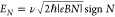 . In a twisted bilayer,
infinite degeneracy
of LLs gives a leeway to the interlayer charge transfer, which screens
out the displacement field and pins partially filled top/bottom layer
LLs, Nt and Nb, to each other and to their common
chemical potential, μ. As a result, we find that
. In a twisted bilayer,
infinite degeneracy
of LLs gives a leeway to the interlayer charge transfer, which screens
out the displacement field and pins partially filled top/bottom layer
LLs, Nt and Nb, to each other and to their common
chemical potential, μ. As a result, we find that 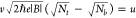 , as sketched in the inset in Figure 2(b). This LL pining
effect
also persists for slightly broadened (e.g., by disorder) LLs. Taking
into account a small Gaussian LL broadening, Γ, we write,
, as sketched in the inset in Figure 2(b). This LL pining
effect
also persists for slightly broadened (e.g., by disorder) LLs. Taking
into account a small Gaussian LL broadening, Γ, we write,
| 6 |
Then, we solve self-consistently eq 1 and compute the total density of states (DoS) in the bilayer. The computed DoS for B = 2 T and Γ ≈ 0.5 meV is mapped in Figure 2(b) versus displacement field and the total tBLG filling factor, νtot = hn/eB (n = nt + nb). Here, the “bright” high-DoS spots indicate the interlayer LL pinning conditions, whereas the “dark” low-DoS streaks mark conditions for incompressible states in a tBLG. We compare this DoS map with ρxx(D, νtot) measured in the quantum Hall effect regime (similar to the ones observed earlier9,10 in other tBLG devices), where the high values of Rxx manifest mutual pinning of partially filled LLs, and the minima correspond to the incompressible states. To mention, the computed pattern broadly varies upon changing ϵz, whereas the value of ϵz = 2.5 gives an excellent match between the computed and measured maps in Figure 2(b).
Electrostatics of Bernal Bilayers
Finally, we analyze the electrostatically
controlled asymmetry
gap1 in BLG, taking into account out-of-plane
polarizability of its constituent monolayers. In this case, we use eq 1 with 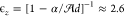 , recalculated from polarizability αDFT using d = 3.35 Å,
and the BLG Hamiltonian1
, recalculated from polarizability αDFT using d = 3.35 Å,
and the BLG Hamiltonian1
 |
7 |
which determines the
dispersion and the sublattice
(A/B) amplitudes,  , in four
(β = 1–4) spin- and
valley-degenerate bands,
, in four
(β = 1–4) spin- and
valley-degenerate bands,  . Here, πξ ≡ ξkx + iky, k =
(kx, ky) is the electron wave vector in the
valleys Kξ = ξ(4π/3a, 0), ξ = ±. The computed sublattice amplitudes,
. Here, πξ ≡ ξkx + iky, k =
(kx, ky) is the electron wave vector in the
valleys Kξ = ξ(4π/3a, 0), ξ = ±. The computed sublattice amplitudes,  , determine
the on-layer electron densities,
which, in an undoped BLG with the Fermi level in the gap between bands
β = 1, 2 and β = 3, 4, are
, determine
the on-layer electron densities,
which, in an undoped BLG with the Fermi level in the gap between bands
β = 1, 2 and β = 3, 4, are
| 8 |
The on-layer potential energy difference, u, and a band gap, Δ, in the BLG spectrum (see inset in Figure 3), computed using self-consistent analysis of eqs 7, 8, and 1 with ϵz = 1 (as in refs (3), (14), and (15)) and with ϵz = 2.6, are plotted in Figure 3 versus displacement field, D. On the same plot, we show the values of lateral transport activation energy36 and the IR “optical gap”—interlayer exciton energy,16 measured earlier in various BLG devices. The difference between those two types of experimentally measured BLG gaps is due to that the single-electron “transport” gap is enhanced by the self-energy correction37 due to the electron–electron repulsion, as compared to the “electrostatic” value, u. In contrast, the interlayer exciton energy has a value close to the interlayer potential difference, u, because self-energy enhancement for electrons and holes is mostly canceled out by the binding energy of the exciton,16,37 an optically active electron–hole bound state. As one can see in Figure 3, u and Δ computed without taking into account a monolayer’s polarizability (ϵz = 1) largely overestimate their values. At the same time, the values of u and Δ obtained using ϵz = 2.6 appear to be less than the exciton energy measured in optics, for interlayer coupling across the whole range 0.35 < γ1 < 0.38 eV covered in the previous literature.34,35,38−42 This discrepancy may be related to that the interaction terms in the electron self-energy are only partially canceled by the exciton binding energy.37 It may also signal that the out-of-plane monolayer polarizability, α, is reduced by ∼10% when it is part of BLG, as the values of Δ computed with ϵz = 2.35 and γ1 = 0.35 eV agree very well with the measured optical gap values.
Figure 3.

Interlayer asymmetry potential (dashed lines) and band gap (solid lines) in an undoped BLG, self-consistently computed with various values of ϵz = 1 (green), 2.6 (blue), and 2.35 (red) and compared to the optical gap measured in ref (16) (circles) and the transport gap33 (crosses). Here, we use34,35v = 10.2 · 106 m/s, γ1 = 0.38 eV, v3 = 1.23 · 105 m/s, v4 = 4.54 · 104 m/s, δ = 22 meV, and d = 3.35 Å. Dotted lines show the values of the gap computed with γ1 = 0.35 eV and the same other parameters. The sketch illustrates four BLG bands (1,2 below and 3,4 above the gap) highlighting a small difference between u and Δ.
In summary, the reported analysis of the out-of-plane dielectric susceptibility of monolayer graphene shows that the latter plays an important role in determining the electrostatics of both Bernal and twisted bilayer graphene. We found that the DFT-computed polarizability of the monolayer, α = 10.8 Å3, accounts very well for all details of the electrostatics of twisted bilayers, including the on-layer electron density distribution at zero magnetic field and the interlayer Landau level pinning at quantizing magnetic fields. For practical applications in modeling of FET devices based on twisted bilayers, the polarizability of monolayer graphene can be converted to its effective dielectric susceptibility, ϵz ≈ 2.5, which should be used for the self-consistent electrostatic analysis of tBLG using eq 1 of this manuscript.
Acknowledgments
This work was supported by EPSRC grants EP/S019367/1, EP/S030719/1, EP/N010345/1, ERC Synergy Grant Hetero2D, a Lloyd Register Foundation Nanotechnology grant, and the European Graphene Flagship Core 3 Project. Computing resources were provided by Lancaster HEC cluster and Manchester SCF.
The authors declare no competing financial interest.
Footnotes
Note that, at larger external fields, the energy abruptly becomes nonquadratic in D due to electronic density appearing in the artificial triangular well of the sawtooth potential, which sets the limits for the applicability of the DFT method we used. Also, we find that α is sensitive to the plane-wave cut-off energy at small external fields, which limits from below the range of D values we used in the analysis. We verified that the same polarizability results were obtained by directly evaluating the change in the dipole moment within the simulation cell when the external field is applied. Note that here we differ from some earlier studies of, e.g., bilayers,18,19 where the dielectric screening contribution has not been separated from the contribution resulting from charge redistribution across the layers.
References
- McCann E.; Fal’ko V. I. Landau-level degeneracy and quantum Hall effect in a graphite bilayer. Phys. Rev. Lett. 2006, 96, 086805. 10.1103/PhysRevLett.96.086805. [DOI] [PubMed] [Google Scholar]
- Novoselov K. S.; McCann E.; Morozov S. V.; Fal’ko V. I.; Katsnelson M. I.; Zeitler U.; Jiang D.; Schedin F.; Geim A. K. Unconventional quantum Hall effect and Berry’s phase of 2π in bilayer graphene. Nat. Phys. 2006, 2, 177. 10.1038/nphys245. [DOI] [Google Scholar]
- McCann E. Asymmetry gap in the electronic band structure of bilayer graphene. Phys. Rev. B: Condens. Matter Mater. Phys. 2006, 74, 161403. 10.1103/PhysRevB.74.161403. [DOI] [Google Scholar]
- Lopes dos Santos J. M. B.; Peres N. M. R.; Castro Neto A. H. Graphene bilayer with a twist: Electronic structure. Phys. Rev. Lett. 2007, 99, 256802. 10.1103/PhysRevLett.99.256802. [DOI] [PubMed] [Google Scholar]
- Bistritzer R.; MacDonald A. H. Moiré bands in twisted double-layer graphene. Proc. Natl. Acad. Sci. U. S. A. 2011, 108, 12233. 10.1073/pnas.1108174108. [DOI] [PMC free article] [PubMed] [Google Scholar]
- Fal'ko V. Graphene - quantum information on chicken wire. Nat. Phys. 2007, 3, 151. 10.1038/nphys556. [DOI] [Google Scholar]
- Kurzmann A.; Overweg H.; Eich M.; Pally A.; Rickhaus P.; Pisoni R.; Lee Y.; Watanabe K.; Taniguchi T.; Ihn T.; Ensslin K. Charge detection in gate-defined bilayer graphene quantum dots. Nano Lett. 2019, 19, 5216. 10.1021/acs.nanolett.9b01617. [DOI] [PubMed] [Google Scholar]
- Seifert P.; Lu X.; Stepanov P.; Durán Retamal J. R.; Moore J. N.; Fong K.-C.; Principi A.; Efetov D. K. Magic-Angle Bilayer Graphene Nanocalorimeters: Toward Broadband, Energy-Resolving Single Photon Detection. Nano Lett. 2020, 20, 3459. 10.1021/acs.nanolett.0c00373. [DOI] [PubMed] [Google Scholar]
- Sanchez-Yamagishi J. D.; Taychatanapat T.; Watanabe K.; Taniguchi T.; Yacoby A.; Jarillo-Herrero P. Quantum Hall effect, screening, and layer-polarized insulating states in twisted bilayer graphene. Phys. Rev. Lett. 2012, 108, 076601. 10.1103/PhysRevLett.108.076601. [DOI] [PubMed] [Google Scholar]
- Fallahazad B.; Hao Y.; Lee K.; Kim S.; Ruoff R. S.; Tutuc E. Quantum Hall effect in Bernal stacked and twisted bilayer graphene grown on Cu by chemical vapor deposition. Phys. Rev. B: Condens. Matter Mater. Phys. 2012, 85, 201408. 10.1103/PhysRevB.85.201408. [DOI] [Google Scholar]
- Slizovskiy S.; Garcia-Ruiz A.; Berdyugin A. I.; Xin N.; Taniguchi T.; Watanabe K.; Geim A. K.; Drummond N. D.; Fal’ko V. I.. Out-of-plane dielectric susceptibility of graphene in twistronic and bernal bilayers. arXiv 2021. https://arxiv.org/pdf/1912.10067.pdf (accessed July 13, 2021). [DOI] [PMC free article] [PubMed] [Google Scholar]
- Rickhaus P.; Liu M.-H.; Kurpas M.; Kurzmann A.; Lee Y.; Overweg H.; Eich M.; Pisoni R.; Taniguchi T.; Watanabe K.; Richter K.; Ensslin K.; Ihn T. The electronic thickness of graphene. Science Advances 2020, 6, eaay8409 10.1126/sciadv.aay8409. [DOI] [PMC free article] [PubMed] [Google Scholar]
- Berdyugin A. I.; Tsim B.; Kumaravadivel P.; Xu S. G.; Ceferino A.; Knothe A.; Kumar R. K.; Taniguchi T.; Watanabe K.; Geim A. K.; Grigorieva I. V.; Fal’ko V. I. Minibands in twisted bilayer graphene probed by magnetic focusing. Science Advances 2020, 6, eaay7838 10.1126/sciadv.aay7838. [DOI] [PMC free article] [PubMed] [Google Scholar]
- Castro Neto A. H.; Guinea F.; Peres N. M. R.; Novoselov K. S.; Geim A. K. The electronic properties of graphene. Rev. Mod. Phys. 2009, 81, 109. 10.1103/RevModPhys.81.109. [DOI] [Google Scholar]
- McCann E.; Koshino M. The electronic properties of bilayer graphene. Rep. Prog. Phys. 2013, 76, 056503. 10.1088/0034-4885/76/5/056503. [DOI] [PubMed] [Google Scholar]
- Ju L.; Wang L.; Cao T.; Taniguchi T.; Watanabe K.; Louie S. G.; Rana F.; Park J.; Hone J.; Wang F.; McEuen P. L. Tunable excitons in bilayer graphene. Science 2017, 358, 907. 10.1126/science.aam9175. [DOI] [PubMed] [Google Scholar]
- Clark S. J.; Segall M. D.; Pickard C. J.; Hasnip P. J.; Probert M. I. J.; Refson K.; Payne M. C. First principles methods using CASTEP. Z. Kristallogr. - Cryst. Mater. 2005, 220, 567. 10.1524/zkri.220.5.567.65075. [DOI] [Google Scholar]
- Yu E. K.; Stewart D. A.; Tiwari S. Ab initio study of polarizability and induced charge densities in multilayer graphene films. Phys. Rev. B: Condens. Matter Mater. Phys. 2008, 77, 195406. 10.1103/PhysRevB.77.195406. [DOI] [Google Scholar]
- Santos E. J. G.; Kaxiras E. Electric-Field Dependence of the Effective Dielectric Constant in Graphene. Nano Lett. 2013, 13, 898. 10.1021/nl303611v. [DOI] [PubMed] [Google Scholar]
- Fang J.; Vandenberghe W. G.; Fischetti M. V. Microscopic dielectric permittivities of graphene nanoribbons and graphene. Phys. Rev. B: Condens. Matter Mater. Phys. 2016, 94, 045318. 10.1103/PhysRevB.94.045318. [DOI] [Google Scholar]
- Foulkes W. M.; Mitas L.; Needs R. J.; Rajagopal G. Quantum Monte Carlo simulations of solids. Rev. Mod. Phys. 2001, 73, 33. 10.1103/RevModPhys.73.33. [DOI] [Google Scholar]
- Ceperley D. M.; Alder B. J. Ground State of the Electron Gas by a Stochastic Method. Phys. Rev. Lett. 1980, 45, 566. 10.1103/PhysRevLett.45.566. [DOI] [Google Scholar]
- Ceperley D. M.; Kalos M. H. Quantum Many-Body Problems. Top. Curr. Phys. 1986, 7, 145. 10.1007/978-3-642-82803-4_4. [DOI] [Google Scholar]
- Lin C.; Zong F. H.; Ceperley D. M. Twist-averaged boundary conditions in continuum quantum monte carlo algorithms. Phys. Rev. E: Stat. Phys., Plasmas, Fluids, Relat. Interdiscip. Top. 2001, 64, 016702. 10.1103/PhysRevE.64.016702. [DOI] [PubMed] [Google Scholar]
- Trail J. R.; Needs R. J. Norm-conserving hartree–fock pseudopotentials and their asymptotic behavior. J. Chem. Phys. 2005, 122, 014112. 10.1063/1.1829049. [DOI] [PubMed] [Google Scholar]
- Trail J. R.; Needs R. J. Erratum: “smooth relativistic hartree-fock pseudopotentials for h to ba and lu to hg” [j. chem. phys. 122, 174109 (2005)]. J. Chem. Phys. 2013, 139, 039902. 10.1063/1.4815913. [DOI] [PubMed] [Google Scholar]
- Needs R. J.; Towler M. D.; Drummond N. D.; López Ríos P.; Trail J. R. Variational and diffusion quantum monte carlo calculations with the casino code. J. Chem. Phys. 2020, 152, 154106. 10.1063/1.5144288. [DOI] [PubMed] [Google Scholar]
- Clark S. J.; Segall M. D.; Pickard C. J.; Hasnip P. J.; Probert M. I. J.; Refson K.; Payne M. C. First principles methods using castep. Z. Kristallogr. - Cryst. Mater. 2005, 220, 567. 10.1524/zkri.220.5.567.65075. [DOI] [Google Scholar]
- Drummond N. D.; Towler M. D.; Needs R. J. Jastrow correlation factor for atoms, molecules, and solids. Phys. Rev. B: Condens. Matter Mater. Phys. 2004, 70, 235119. 10.1103/PhysRevB.70.235119. [DOI] [Google Scholar]
- Umrigar C. J.; Toulouse J.; Filippi C.; Sorella S.; Hennig R. G. Alleviation of the fermion-sign problem by optimization of many-body wave functions. Phys. Rev. Lett. 2007, 98, 110201. 10.1103/PhysRevLett.98.110201. [DOI] [PubMed] [Google Scholar]
- Bayot V.; Piraux L.; Michenaud J.-P.; Issi J.-P.; Lelaurain M.; Moore A. Two-dimensional weak localization in partially graphitic carbons. Phys. Rev. B: Condens. Matter Mater. Phys. 1990, 41, 11770. 10.1103/PhysRevB.41.11770. [DOI] [PubMed] [Google Scholar]
- Cheianov V. V.; Fal’ko V. I. Friedel oscillations, impurity scattering, and temperature dependence of resistivity in graphene. Phys. Rev. Lett. 2006, 97, 226801. 10.1103/PhysRevLett.97.226801. [DOI] [PubMed] [Google Scholar]
- Zhang Y.; Tang T.-T.; Girit C.; Hao Z.; Martin M. C.; Zettl A.; Crommie M. F.; Shen Y. R.; Wang F. Direct observation of a widely tunable bandgap in bilayer graphene. Nature (London, U. K.) 2009, 459, 820. 10.1038/nature08105. [DOI] [PubMed] [Google Scholar]
- Kuzmenko A. B.; Crassee I.; van der Marel D.; Blake P.; Novoselov K. S. Determination of the gate-tunable bandgap and tightbinding parameters in bilayer graphene using infrared spectroscopy. Phys. Rev. B: Condens. Matter Mater. Phys. 2009, 80, 165406. 10.1103/PhysRevB.80.165406. [DOI] [Google Scholar]
- Joucken F.; Ge Z.; Quezada-López E. A.; Davenport J. L.; Watanabe K.; Taniguchi T.; Velasco J. Determination of the trigonal warping orientation in Bernal-stacked bilayer graphene via scanning tunneling microscopy. Phys. Rev. B: Condens. Matter Mater. Phys. 2020, 101, 161103. 10.1103/PhysRevB.101.161103. [DOI] [Google Scholar]
- Zhang L. M.; Li Z. Q.; Basov D. N.; Fogler M. M.; Hao Z.; Martin M. C. Determination of the electronic structure of bilayer graphene from infrared spectroscopy. Phys. Rev. B: Condens. Matter Mater. Phys. 2008, 78, 235408. 10.1103/PhysRevB.78.235408. [DOI] [Google Scholar]
- Cheianov V. V.; Aleiner I. L.; Fal’ko V. I. Gapped bilayer graphene: A tunable strongly correlated band insulator. Phys. Rev. Lett. 2012, 109, 106801. 10.1103/PhysRevLett.109.106801. [DOI] [PubMed] [Google Scholar]
- Mak K. F.; Lui C. H.; Shan J.; Heinz T. F. Observation of an electric-field-induced band gap in bilayer graphene by infrared spectroscopy. Phys. Rev. Lett. 2009, 102, 256405. 10.1103/PhysRevLett.102.256405. [DOI] [PubMed] [Google Scholar]
- Wirth K. G.; Linnenbank H.; Steinle T.; Banszerus L.; Icking E.; Stampfer C.; Giessen H.; Taubner T. Tunable s-snom for nanoscale infrared optical measurement of electronic properties of bilayer graphene. ACS Photonics 2021, 8, 418. 10.1021/acsphotonics.0c01442. [DOI] [PMC free article] [PubMed] [Google Scholar]
- Min H.; Sahu B.; Banerjee S. K.; MacDonald A. H. Ab initio theory of gate induced gaps in graphene bilayers. Phys. Rev. B: Condens. Matter Mater. Phys. 2007, 75, 155115. 10.1103/PhysRevB.75.155115. [DOI] [Google Scholar]
- Jung J.; MacDonald A. H. Accurate tight-binding models for the π bands of bilayer graphene. Phys. Rev. B: Condens. Matter Mater. Phys. 2014, 89, 035405. 10.1103/PhysRevB.89.035405. [DOI] [Google Scholar]
- Candussio S.; Durnev M. V.; Slizovskiy S.; Jötten T.; Keil J.; Bel’kov V. V.; Yin J.; Yang Y.; Son S.-K.; Mishchenko A.; Fal’ko V.; Ganichev S. D. Edge photocurrent in bilayer graphene due to inter-landau-level transitions. Phys. Rev. B: Condens. Matter Mater. Phys. 2021, 103, 125408. 10.1103/PhysRevB.103.125408. [DOI] [Google Scholar]