

Abstract
Incorporating extended pi‐conjugated organic cations in layered lead halide perovskites is a recent trend promising to merge the fields of organic semiconductors and lead halide perovskites. Herein, we integrate benzodithiophene (BDT) into Ruddlesden–Popper (RP) layered and quasi‐layered lead iodide thin films (with methylammonium, MA) of the form (BDT)2MAn−1PbnI3n+1. The importance of tuning the ligand chemical structure is shown as an alkyl chain length of at least six carbon atoms is required to form a photoactive RP (n=1) phase. With N=20 or 100, as prepared in the precursor solution following the formula (BDT)2MAN−1PbNI3N+1, the performance and stability of devices surpassed those with phenylethylammonium (PEA). For N=100, the BDT cation gave a power conversion efficiency of up to 14.7 % vs. 13.7 % with PEA. Transient photocurrent, UV photoelectron spectroscopy, and Fourier transform infrared spectroscopy point to improved charge transport in the device active layer and additional electronic states close to the valence band, suggesting the formation of a Lewis adduct between the BDT and surface iodide vacancies.
Keywords: 2D perovskites, device stability, Lewis adducts, organic semiconductors, photovoltaic devices
Siding with another: Side‐chain‐engineered benzodithiopheneammonium (BDT) molecules are shown to be excellent ligands for layered halide perovskites. Tailoring the side chain was found to be crucial in order to obtain crystalline structures whereas the highly conjugated BDT core and its sulfur‐containing moieties afford enhanced photovoltaic charge collection, conversion efficiency, and stability when juxtaposed with conventional phenylethylammonium‐based layered perovskites.
Introduction
Layered hybrid organic–inorganic lead halide perovskites (commonly called 2D perovskites) have recently emerged as promising advanced semiconductors to replace the traditional pseudo‐cubic “3D” lead halide perovskites in applications such as solar cells, photodetectors, and light emitting diodes, since they offer significantly improved stability and greater tunability of optoelectronic properties.[1, 2, 3, 4, 5] The structure of the most‐commonly studied layered lead halide perovskites (i. e., the Ruddlesden–Popper, RP, phase) consists of sheets of corner‐sharing PbX6 octahedra (X=Cl, Br, I) separated by layers of bulky monocation‐functionalized organic spacers, R, giving a chemical formula of (R)2PbX4 that can be simply prepared as thin films using solution‐based methods. Layered lead halide perovskites (LLHPs) formed from typical R cations including butylammonium (BA) and phenylethylammonium (PEA) have been extensively studied in device applications, both in their pure RP phase form and in quasi‐layered structures where the number of inorganic layers (n) is increased relative to the organic; the latter increases the light absorption and charge carrier transport since BA and PEA are optically transparent and electrically insulating.[6, 7, 8, 9, 10, 11] Indeed, while a multitude of optoelectronically‐innocent organic spacers have been reported in LLHPs, an exciting emergent trend is the incorporation of aromatic moieties with extended π‐conjugation that can offer supplementary semiconducting properties such as controlled electronic conductivity, increased light absorption, enhanced photo‐induced charge transfer, and tunable quantum well electronic structures.[12] This trend has been inspired by the success of molecular engineering in the field of organic semiconductors, where judicious design has afforded unprecedented tunability of material properties.[13] To this end, cation‐functionalized organic semiconductor building blocks based on pyrene,[14, 15, 16] perylene,[17, 18] carbazole,[19] and thiophene,[20, 21, 22] have been reported recently in layered and quasi‐layered hybrid perovskites.
While these demonstrations are encouraging steps towards merging the fields of organic electronics and hybrid perovskites, the ability to successfully incorporate conjugated organics in LLHPs is severely limited by their size and their intermolecular pi‐pi stacking. Indeed, the size of the PbX6 octahedra defines a constraint on the width/depth of the organic. Moreover, the presence of an increasing number of heteroatoms (sulfur and nitrogen) in the aromatic structure, which is generally favorable for the semiconducting properties,[23] also increases the strength of the pi‐pi interactions[24, 25] disrupting the formation of LLHPs via self‐aggregation of the organic. Recently, Dou and co‐workers engineered steric effects in a benzothiadiazole‐containing cation to reduce π‐stacking and facilitate incorporation.[26] While this approach allowed the integration of an impressively long conjugated system, the use of steric hinderance also reduces the intermolecular conjugation and limits the extent of energy level control in the organic. Thus, there remains a need to develop strategies and understanding towards the incorporation of large, rigid, and heteroatom‐containing conjugated organic cations in LLHPs. Progress can be made in this aspect by continuing to demonstrate the incorporation of diverse organic semiconductor building blocks in LLHPs and by recognizing how to engineer their incorporation via structural modification.
Benzodithiophene (BDT) is a widely successful planar conjugated building block in the field of organic semiconductors due to its excellent semiconducting properties and its ease of synthesis and functionalization.[27] However, its incorporation in LLHPs has not been reported to our knowledge. In view of the known ability of electron‐donating thiophene‐based small molecules as passivating agents for defects in the perovskite structure,[28, 29, 30] we further hypothesized that the incorporation of a BDT‐based cation in LLHPs in the layered or quasi‐layered structure, if possible, could also act to passivate halide defects via a Lewis base mechanism. Herein, we prepare BDT‐based cations with different alkane linkers and find that the linker length is critical for incorporation into LLHPs. Furthermore, via incorporation into photovoltaic devices in a quasi‐layered structure, and in comparison to the standard PEA‐based spacer, we present evidence for an additional passivation mechanism in the BDT‐based system.
Results and Discussion
Benzodithiophene incorporation in layered perovskites
To demonstrate the incorporation of the conjugated BDT core we first hypothesized that the length of an alkyl chain linking the BDT to an aminium ion (commonly called ammonium) could be an important factor. To test this, we prepared three versions of the iodide salts of m‐(benzo[1,2‐b:4,5‐b′]dithiophen‐2‐yl)alkan‐1‐aminium with m=2,4,6 (see chemical structures in Figure 1a) using the synthesis routes described in Schemes S1 and S2 (Supporting Information) to yield the cations coded as BDT‐C2, BDT‐C4, and BDT‐C6 for 2, 4, and 6 carbon linkers, respectively. To form (BDT‐Cm)2PbI4 thin films, stoichiometric amounts of the BDT iodide salts were dissolved with PbI2 in DMF at 0.1 M, spin coated, and annealed at 130 °C for 10 min. X‐ray diffraction of the (BDT‐Cm)2PbI4 thin films prepared on glass substrates reveals a significant difference in crystallinity with respect to the number of carbon atoms (Figure 1b, Table S1 in the Supporting Information). Indeed, while the (BDT‐C6)2PbI4 thin film showed clear and intense diffraction peaks which can be indexed to a RP phase, peaks for the BDT‐C4 version were drastically diminished and no RP phase peaks were evident on the BDT‐C2‐based film. The absence of a strong diffraction peak around 2θ=12.5° for all BDT cations discounts the formation of crystalline PbI2 domains, suggesting a homogeneous mixture of the organic cation and lead iodide even for the BDT‐C2‐based film. Interestingly, the UV/Vis absorption spectrum of the BDT‐C2‐based film (Figure 1c) shows an extended absorption shoulder until ∼700 nm, similar to drop‐cast films of pure BDT.[31] Indeed, the absorption spectrum for the BDT‐C2 drop‐cast film alone shows an absorption shoulder, also evident of extended j‐aggregation, which is no longer present in the BDT‐C4 and BDT‐C6 drop‐cast films (Figure S1). The absence of this absorption shoulder in the BDT‐C4‐ and the BDT‐C6‐ based films further supports their formation of a RP phase without an extended π–π stacking of the BDT cation. Despite the characteristic, though weaker, XRD peaks of a RP phase, the (BDT‐C4)2PbI4 thin film does not exhibit the distinctive excitonic UV/Vis absorption peak of a LLHP and no photoluminescence (PL) was observed from this film. In contrast, the (BDT‐C6)2PbI4 thin film shows a clear absorption peak at 490 nm and a strong PL emission was observed centered at 510 nm. These features are hypsochromic to (PEA)2PbI4 (Figure S2) suggesting that the conjugated BDT core is optoelectronically‐uncoupled from the layers of lead iodide—consistent with a larger separation distance expected from the hexyl‐linker in BDT‐C6. Additional information on the crystallinity of the BDT‐based LLHPs is given by grazing incidence wide angle X‐ray scattering (GIWAXS) diffraction patterns (Figure 1d), which confirm the strong out‐of‐plane orientation for (BDT‐C6)2PbI4 with the (00 l) planes oriented parallel to the substrate. The (BDT‐C4)2PbI4 film shows a similar orientation despite its poorer crystallinity, while the amorphous nature of the (BDT‐C2)2PbI4 is confirmed. Overall, the XRD and GIWAXS data of the (BDT‐C6)2PbI4 film suggest an interlayer spacing of 22.9 Å. Considering this distance and the BDT‐C6 molecular length of 16.1 Å (obtained via DFT calculations with SCIGRESSTM v.3.4.3) an overlapping of the BDT core is inferred consistent with the schematic structure shown in Figure 1e, where π–π interactions between opposite BDT units are influential towards the interlayer spacing. However, as forming single crystals of (BDT‐C6)2PbI4 was not possible despite significant efforts, further insight into the precise hexyl chain orientation and pi‐pi interactions of the BDT core in the RP phase are out of the scope of this work. Despite this, the effect of the changing alkyl chain length remains a significant observation and suggests an important design rule for incorporating rigid conjugated moieties in LLHPs.
Figure 1.
(a) Benzodithiophene‐based ligand chemical structures where m represents the number of carbon atoms in the alkyl chain between the aminium cation and the conjugated BDT core. (b) X‐ray diffraction patterns of (BDT‐Cm)2PbI4 thin films and (c) corresponding UV/Vis absorption and photoluminescence spectra. Note that PL is only observed for (BDT‐C6)2PbI4. (d) GIWAXS patterns of (BDT‐Cm)2PbI4 thin films. (e) Schematic of a proposed layer arrangement of the (BDT‐C6)2PbI4 perovskite (drawn with the Vesta software[34]). (f) J–V curve for a (BDT‐C6)2PbI4 ‐based photovoltaic device under 1 sun illumination (energy levels of the device in the inset). For BDT‐C22PbI4, the formula denotes the stoichiometry of the fabrication solution and not the final crystal, which is not formed.
Considering the success at incorporating the BDT‐C6 cation into a RP LLHP, we gathered additional data on this version for further optoelectronic application (Figure S3). The optical band gap of (BDT‐C6)2PbI4 was found to be 2.40 eV via Tauc plot analysis compared to 2.36 eV for (PEA)2PbI4. In addition, the valence band maxima were determined by ultraviolet photoelectron spectroscopy (UPS) measurements following linear extrapolations for the valence band maximum (VBM), secondary electron cut‐off and the corresponding ionization energy calculations.[32, 33] These data were combined to locate the VBM of (BDT‐C6)2PbI4 at 5.7 eV vs. vacuum compared to 6.0 eV for PEA2PbI4 (Figure S3e).
The good crystallinity, strong PL and suitable energy levels of the (BDT‐C6)2PbI4 were next put to test in a standard n‐i‐p photovoltaic device with a fluorine‐doped tin oxide (FTO) substrate, compact+mesoporous TiO2 as the electron transport layer (ETL), Spiro‐OMeTAD as the hole transporting layer (HTL), and Au as the top electrode. Figure 1f shows the energy level alignment of the device and the best current density–voltage (J–V) curves under 1 sun illumination, which showed negligible hysteresis between forward and reverse scans. However, generally low performance parameters were observed with a short circuit current density, J SC=1.9 mA cm−2, open circuit potential, V OC=0.46 V, and a fill factor, FF=0.5, resulting in a power conversion efficiency of only 0.42 %. This modest performance is similar to other “single‐layered” LLHPs[4] and is limited by the alignment of the layers parallel with the substrate, which prevents charge transport to the electrodes of the device.
Quasi‐layered photovoltaic devices
Increasing the number of inorganic layers, n, with respect to the bulky organic cation as represented by the chemical formula (R)2An−1PbnX3n+1, where A is a small organic cation (e. g., MA=methylammonium) to yield a quasi‐layered semiconductor material is a well‐established route to improve the performance of LLHP‐based solar cells. Indeed, quasi‐layered lead halide perovskites (QLLHPs) exhibit a reduction in band gap energy, smaller exciton binding energy, and improved layer orientation with respect to the substrate compared to LLHPs (where n=1), while generally also improving active layer stability versus their bulk counterparts (n=∞).[35, 36, 37]
Thus, we next investigated the performance of the BDT‐C6 cation (referred to hereafter as the BDT cation for simplicity) compared to the standard PEA cation in quasi‐layered solar cells, following the formulas (BDT)2MAN−1PbNI3N+1 and (PEA)2MAN−1PbNI3N+1, respectively in the precursor solution preparation. While we did not focus on quasi‐layered cells with N<20 due to poor morphology, we noted a significant performance difference for medium and high N numbers which are represented by N=20 and 100, respectively. To prepare thin films of the quasi‐layered lead halide perovskites (QLLHPs) we employed the antisolvent approach shown schematically in Figure S4. We denote the (BDT)2MAN−1PbNI3N+1 films as N20 MBDT and N100 MBDT for N=20 and 100, respectively, and similarly for N20 MPEA and N100 MPEA to simplify the compositional notation for the reader. Although the XRD patterns of both the N20 and N100 series of perovskites with BDT and PEA ligands exhibit mainly the principal MAPbI3 phase due to its majority content (see Figure S5a and b) similar to comparable reports,[9, 38] high‐resolution transmission electron microscopy, HRTEM, measurements (See Figure S6) and corresponding fast Fourier transforms (FFT) of the N20 and N100 films indicate regions with interlayer spacings of 7.4 and 7.8 Å for MPEA and MBDT, respectively, suggesting the presence of low n layered domains existing together with n=∞ domains (with interlayer spacing of 3.1 Å), similar to a previously‐described QLLHP with butylammonium.[39] In addition, a homogeneous distribution of sulfur, lead, and iodide is observed on a >100 nm length scale throughout a portion of an N20 MBDT film with transmission electron microscopy with energy dispersive X‐ray spectroscopy (TEM‐EDX), suggesting that the BDT cation is evenly distributed in the film (Figure S7). Photoluminescence (PL) measurements also indicate the formation of the QLLHPs (Figure S8), where hypsochromic shifts of the emission maximum wavelength are observed for the N20 and N100 MBDT and MPEA samples, with respect to the MAPbI3 reference, further supporting the existence of homogeneously distributed bulky cations in the quasi‐layered film.
In order to compare the photovoltaic performance of the BDT‐based QLLHP to the PEA version, devices were next fabricated: FTO/TiO2/QLLHP/Spiro/Au. Band alignments with the electron and hole contacts[40] and energy levels of the QLLHP used are presented in Figure 2a (note only one of the four active materials was used for each device). The bandgap energies were determined from UV/Vis spectra (Figure S9) and the corresponding Tauc plots (Figure S10). The valence band maxima (VBM) energy levels with respect to vacuum were deduced from UPS linear extrapolations for the VBM (Figure S11), secondary electron cut‐off (Figure S12), and the corresponding ionization energy calculations (Figure S13).[32, 33] The 1 sun J–V curves of the best‐performing devices for each of the active layers are reported in Figure 2b.
Figure 2.
Quasi‐layered devices. (a) Energy level and band gap alignment of the four QLLHP materials tested (inside the dashed box) with respect to the hole‐transporting and electron‐transporting contacts used. (b) Champion cell J–V curves obtained with a 0.09 cm2 active area and AM 1.5G illumination. (c) Box plots with results of 20 devices for each QLLHP material and (d) device incident photon‐to‐current efficiency (IPCE) and integrated currents with respect to illumination wavelength.
For the N100 series, the N100 MBDT device outperforms N100 MPEA with a PCE of 14.7 % vs. 13.7 %, which is mainly due to an enhanced J SC and a moderate FF increase. We note that the performance of the MPEA devices is comparable to previous reports with similar n,[41] but slightly lower likely due to the larger aperture area (0.09 cm2 vs. 0.05 cm2) used in our work. The enhancement of the J SC of the BDT vs. that of the PEA QLLHP becomes more evident at lower N values, where the N20 MBDT best‐performing device resulted in a PCE of 8.5 % vs. 5.3 % for the best N20 MPEA device. It is worth noting that the observed higher J SC values in the BDT‐based devices are not due to a light absorption increase, as the PEA and BDT devices exhibited similar light absorbance (Figure S9). In addition to the best‐performing devices, both the N20 and the N100 MBDT devices display a more reproducible and narrower device PCE distribution compared to the N20 and N100 MPEA devices, respectively, as shown by box plots presented in Figure 2c representing the PCE results from 20 devices prepared for each material tested (average and champion values for J SC, V OC, and FF are listed in Table 1). Moreover, we note that hysteresis decreases significantly for higher N number perovskites (Figure S14, Table S2). The J SC, V OC and FF distributions for all devices are displayed in more detail on Figure S15. To further verify the performance of the MBDT and MPEA devices, the incident photon to current efficiency (IPCE) was measured as a function of illumination wavelength at short‐circuit conditions (Figure 2d). Integrating the data with the standard solar spectrum resulted in theoretical one‐sun J SC values of 22.36 mA cm−2 for N100 MBDT, 19.28 mA cm−2 for N100 MPEA, 15.56 mA cm−2 for N20 MBDT and 13.10 mA cm−2 for N20 MPEA, which match well with the J SC found in the J–V curves.
Table 1.
Comparative numerical photovoltaic results for QLLHP‐based solar cells (reverse scans).
|
Solar cell |
JSC [mA cm−2][a] |
VOC [V][a] |
FF [a] |
PCE [%][a] |
JSC [mA cm−2][b] |
VOC [V][b] |
FF [b] |
PCE [%][b] |
|---|---|---|---|---|---|---|---|---|
|
N20 MBDT |
15.91 |
0.96 |
0.50 |
7.80 |
16.51 |
0.97 |
0.50 |
8.48 |
|
N20 MPEA |
10.46 |
1.02 |
0.40 |
4.07 |
11.66 |
1.01 |
0.48 |
5.27 |
|
N100 MBDT |
22.03 |
1.00 |
0.61 |
13.22 |
24.25 |
1.02 |
0.65 |
14.67 |
|
N100 MPEA |
21.24 |
1.01 |
0.54 |
11.24 |
22.74 |
1.02 |
0.59 |
13.68 |
[a] Average over 20 devices. [b] Champion device.
Origin of the device performance difference
In an effort to rationalize the performance difference between the BDT and PEA QLLHP solar cells we first examined the morphology of the active layer. Interestingly, despite the identical processing conditions, we observed a significantly different morphology of the active layer with scanning electron microscopy (SEM) showing a considerably smaller grain size for the BDT‐containing QLLHP active layers compared to PEA. This is illustrated by the cross‐sectional images for N20 QLLHP layers prepared on FTO and capped with Au shown in Figure 3a, and the top‐down SEM images for the bare films shown in Figure S16 for both the N20 and N100 films, together with the cross‐sectional images of the latter. For the N20 case, the average grain size was calculated to be 153±48 nm for N20 MBDT and 227±58 nm for N20 MPEA. This trend is consistent in the N100 devices where 182±37 nm and 291±86 nm was calculated for the BDT‐ and PEA‐ containing films, respectively. The significantly smaller grain size for the BDT‐containing active layer could result from the lower solubility of this cation in the DMF/DMSO solvent mixture (53 mg mL−1) compared to PEA (83 mg mL−1), leading to a greater amount of seeding during film formation and hence smaller grain size. However, despite the smaller grain size and the associated increased density of grain boundaries, which are a well‐known source of defects and charge carrier traps,[42] the performance of the BDT‐containing devices is improved compared to that of the PEA‐based devices.
Figure 3.
(a) Cross‐sectional SEM images of N20 MBDT(top) and N20 MPEA layers solution‐processed onto FTO substrates and capped with an Au overlayer (to facilitate measurement). (b) Normalized device photocurrent as a function of time after a 5 ns pulse (550 nm wavelength) shown in the log scale over the long‐time frame and a linear scale for the short time regime (inset). (c) UV photoelectron spectroscopy measurements of the perovskite thin films deposited on FTO substrates. The inset shows a schematic of hypothesized undercoordinated Pb passivation via –S (thiophene) Lewis adduct formation (d) ATR‐FTIR data for a BDT drop cast film, BDT2PbI4, N20 MBDT, N100 MBDT and MAPbI3 reference thin films with a highlight of the C−S stretch peak shift, the asterisks represent the peak positions.
Considering that PEA addition to lead halide perovskites is known to passivate defects at the grain boundaries,[9] and knowing that the BDT cation results in more grain boundaries, we hypothesized that the BDT offers an altered passivation of defects in the device active layer. To investigate this possibility, we performed transient photocurrent (TPC) measurements at short circuit conditions using a 5 ns pulsed laser (550 nm wavelength) at a fluence of 0.96 μJ cm−2. The TPC dynamics for representative devices with each active layer are shown in Figure 3b over two time scales (short time response in the inset). While the TPC decay dynamics have been determined to be influenced by both the charge carrier transport in the device and the recombination at the transport layers/absorber interfaces,[43] given the identical charge transport layers in our devices, we attribute differences in the TPC dynamics mainly toward charge transport in the active layer. The extracted TPC exponential decay times (τ c) are given in Table S2 for short and long‐time scales (τ c1 and τ c2, respectively), and a significantly faster decay for the BDT‐containing devices is seen over both time scales as also evident from qualitative inspection of Figure 3b (e. g., τ c1=2.17 and 8.93 μs for the N100 MBDT and MPEA, respectively). These consistently faster decays, together with the larger J SC of the devices, are in line with the view that charge carrier transport is improved in the BDT‐containing devices over a wide range of photogenerated charge densities in the device.[44, 45] This would be expected if charge trapping states at the grain boundaries are energetically altered when the BDT ligand is employed.
Insights into energetic differences of the trapping states at the grain boundaries was next sought by examining the UV photoelectron spectra for the different active layers (Figure 3c) near the valence band maximum (VBM). While the region between the VBM, which is at a binding energy of approximately 1.5 eV, and the Fermi energy level (E F=0 eV) is expected to contain band tail states, an increased density of states in this region (closer to the E F) is observed for both the N20 and N100 MBDT layers compared to the MPEA. Previously, a similar increase in the UPS signal in this region has been attributed to the presence of metallic/reduced Pb species.[46] However, X‐ray Photoelectron Spectroscopy (XPS) measurements did not reveal the presence of metallic Pb nor a loss of Pb cationic character on the octahedral central Pb ion (Figure S17). This is not unexpected given the differences in probing depth (i. e., approximately 5 nm for XPS compared to the ca. 1 nm for UPS) suggesting the observed states are localized at the surface and grain boundaries. In view of the electron‐donating nature of the BDT cation via the sulfur atom in the thiophene,[28, 30] and the frequent presence of iodide vacancies ( in Kröger–Vink notation) at the surface,[47, 48] it is plausible to propose the existence of Lewis acid–base interactions between the BDT cation and the undercoordinated Pb atoms in the vicinity. Given the positive charge on the aforementioned vacancies and their corresponding function as electron traps, forming –S (thiophene) adducts as shown in Figure 3c (inset schematic) could alleviate such defects.
In order to support our observations of reduced Pb species on the UPS measurements on Figure 3c, we have carried out attenuated total reflectance–Fourier transform infrared spectroscopy (ATR‐FTIR) measurements on a pure BDT‐C6 sample, BDT2PbI4, N20 MBDT, N100 MBDT and an MAPbI3 reference sample (Figure 3d). From the resulting spectra, a clear shift of the 652 cm−1 C−S stretch peak in the pure BDT sample towards lower wavenumbers for all the perovskite samples synthesized with BDT can be observed.[49] Namely, in BDT2PbI4, the peak shifts towards 651.0 cm−1 while for N20 MBDT and N100 MBDT, the peak shifts to 650.0 cm−1 and 646.5 cm−1, respectively. The shift towards lower wavenumbers indicates the weakening of the C−S (thiophene) bond which aligns well with the participation of S (thiophene) as an electron‐donating species. Bearing in mind that UPS revealed the partial reduction of Pb in the presence of BDT, it is plausible to consider that the S (thiophene) acts as a Lewis base‐donating electrons to the undercoordinated Pb centers. The results obtained from UPS and ATR‐FTIR data thus support the formation of a Pb–S Lewis adduct. Indeed, similar shifts towards lower wavenumbers have been reported for Lewis acid–base adducts passivating undercoordinated lead defects.[50, 51]
We further speculate that these resulting energy states improve the charge carrier transport between grain boundaries and between the active layer and the hole transporting Spiro overlayer, which could be possible if a formed Lewis adduct brings the BDT moiety into an improved electronic communication with the perovskite material. Indeed, an increased charge carrier transport at these grain boundaries reasonably explains the increased performance of the BDT‐containing devices despite the increased concentration of grain boundaries. Moreover, since BDT is known to operate as a good hole transport moiety in OPV devices, and the “Lewis‐adduct” energy states observed by UPS are well aligned with the energy level of Spiro, an improved hole transfer of the MBDT films to Spiro is a reasonable conclusion.
Device stability comparison
Since the formation of QLLHPs is a well‐established route to increase device stability by preventing ionic migration in the active layer and also the diffusion of water molecules,[4] we next probed the effect of the BDT cation's bulkier nature compared to PEA on the stability of solar cells. The N100 series of devices were subjected to photovoltaic stability measurements in a dry N2 environment under constant one‐sun illumination and the N100 MBDT device showed a significantly improved performance after 130 h, conserving 64 % of the initial performance while the N100 MPEA device conserved only 31 % of its initial performance (Figure 4a). In comparison, an MAPbI3 (n=∞) device dropped to 34 % of the initial performance after only 48 h. The normalized performance parameters for the J SC, V OC, and FF can be found on Figure S18. Under these conditions (dry N2), the enhanced stability of the MBDT device is reasonably ascribed to an improved ability of the bulkier pi‐conjugated BDT cation to suppress MA leakage from the main perovskite (n=∞) domains in the active layer.[52, 53] The N100 QLLHP active layers were also submitted to high humidity environments (75 % relative humidity, RH) for 8 weeks, and examined periodically by XRD to track the phase stability (Figure 4b). After 4 weeks the N100 MPEA samples began to show signs of degradation with the emergence of a new peak at around 2θ=12.5°, indicative of PbI2 segregation from the main perovskite phase, which was not observed for the N100 MBDT perovskite. The improved resistance to water was further confirmed by contact angle measurements (Figure 4c), where an enhanced hydrophobicity was observed for the N100 MBDT (exhibiting a water contact angle of 90.6° compared to 75.4° for the N100 MPEA). Overall, these experiments support the view that the bulky BDT, when incorporated into a QLLHP even at a small quantity (i. e., at N=100) can successfully improve both material and device stabilities compared to the standard PEA cation.
Figure 4.
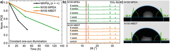
QLLHP stability and moisture resistance measurements. (a) Normalized PCE of the N100‐based devices (and an n=∞ control) with respect to time in a dry N2 environment under constant 1 sun illumination (open‐circuit conditions). (b) XRD patterns of bare QLLHP active layers exposed to 75 % RH air (25 °C) for different times. (c) Water contact angle measurements for bare films of N100 MPEA (top) and N100 MBDT (bottom).
Conclusion
Motivated by the aspiration to integrate diverse organic semiconductor species into layered perovskites we have demonstrated the incorporation of a benzodithiophene (BDT)‐based organic cation in layered and quasi‐layered lead halide perovskites. We found that tuning the length of the alkyl chain between the BDT group and the ammonium ion was critical to the successful formation of a Ruddlesden–Popper (n=1) phase, with only the hexyl BDT‐C6 version resulting in a photoactive RP phase. The resulting (BDT‐C6)2PbI4 perovskite thin films were found to form with layers parallel to the substrate and gave modest photovoltaic device performance. In contrast, the active BDT cation gave superior device performance compared to phenylethylammonium (PEA) in quasi‐layered lead iodide‐based devices with N=20 or 100, due to an increase in JSC . The increased performance, despite a smaller domain size and increase in grain boundaries in the BDT‐containing active layers, was correlated to a faster transient photocurrent (TPC) decay time likely due to superior charge transport/transfer in the BDT devices compared to PEA. In fact, N20‐fabricated perovskite photovoltaic devices with BDT display an increase of 60 % of the performance of the corresponding PEA devices, whereas the N100 devices lead to a performance increase of 8 % of that from the corresponding PEA devices. Moreover, evidence of Lewis acid–base interactions between the BDT cation and undercoordinated Pb atoms (likely present due to iodide vacancies at grain boundaries and active layer interfaces) as acquired by UPS and ATR‐FTIR data, suggests an electronic influence of the BDT cation on the defects and rationalizes the improved performance. In addition, due to its bulkier nature, the BDT‐cation‐based photovoltaic devices showed an increased device stability compared to PEA‐based devices. We further note that only a small BDT cation loading is enough for material stabilization, harnessing the advantages of the better‐performing high‐N‐number perovskites. These results underline both the importance of molecular engineering of π‐conjugated organic cations to tune their ability of incorporation in layered lead halide perovskite thin films. The findings further highlight the possibility to harness functionality in π‐conjugated organic cations to improve performance in layered and quasi‐layered lead halide perovskite solar cells.
Experimental Section
Chemicals and materials employed
PbI2 (99.999 %, Sigma–Aldrich), methylammonium iodide (Greatcell solar), phenylethylammonium iodide (Sigma–Aldrich), N,N‐dimethylformamide (extra dry, 99.8 %, Acros Organics), dimethyl sulfoxide (>99.5 %, Sigma–Aldrich), ethyl acetate (anhydrous, 99.8 %, Sigma Aldrich), chlorobenzene (extra dry, 99.8 %, Acros Organics), Spiro‐MeOTAD (Luminescence Technology Corp), LiTFSI (99.95 %, Sigma–Aldrich), 4‐tert‐butylpyridine (>96 %, TCI), acetonitrile (anhydrous, 99.8 %, Sigma–Aldrich), TiO2 paste (18 NR‐T, Greatcell Solar), titanium(IV) isopropoxide (>97 %, Sigma–Aldrich), PEDOT:PSS (M124 HTL Solar, Ossila), benzo[1,2‐b:4,5‐b′]dithiophene (BDT, TCI, 98 %), n‐butyllithium solution (n‐BuLi, 1.6 M in hexane, Sigma–Aldrich), 1,4‐dibromobutane (Fluorochem, 99 %), 1,6‐dibromohexane (Fluorochem, 95 %), ammonium acetate (ABCR, 97 %), nitromethane (Sigma‐Aldrich, 95 %), lithium aluminum hydride (LiAlH4, Sigma–Aldrich, 95 %), potassium phthalimide (Sigma–Aldrich, 98 %), and hydrazine hydrate (Alfa Aesar, 98 %) were used as received. Conductive patterned FTO was purchased from Lyoyang Guluo Glass Co. with a resistance of 7 Ω/sq.
BDT cation synthesis
BDT cation synthesis reactions were adapted from literature reports[54] and are described in detail in Scheme S1 for BDT‐C2 and Scheme S2 for BDT‐C4 and BDT‐C6.[55] Characterizations of the final cations and reaction intermediates by 1H NMR spectroscopy are given in Figures S19 and S20, for BDT‐C2, in Figures S21 and S22 for BDT‐C4, and finally in Figures S23 and S24 for BDT‐C6. All reactions were carried out under an inert Ar atmosphere unless otherwise specified. The 1H NMR spectra were obtained at room temperature using CDCl3 as internal standard on a 400 MHz NMR Bruker AVANCE III‐400 spectrometer (Bruker, Rheinstetten, Germany). Tetrahydrofuran (THF) and DMF were purified using a Pure Solv‐MD solvent purification system (Innovative Technology, Amesbury, United States). Silica gel chromatography was carried out with technical grade silicon dioxide (Acros Organics, pore size 60 Å and 40–50 μm particle size).
Perovskite thin film fabrication
For MAPbI3, the procedure reported by Huang et al.[56] was followed, namely 1.6 M solutions with 1 : 1 ratio of PbI2/MAI were prepared in a 8.9 : 1.1 (v/v) DMF/DMSO mixture. For the QLLHPs, the PEA or BDT ligands were mixed with PbI2 and methylammonium iodide (MAI) according to the specified stoichiometry. All perovskite solutions were spin coated in an Argon environment with a two‐step program: namely, a first step of 3000 rpm for 10 s, followed by 6000 rpm for 25 s at the beginning of which 500 μL of chlorobenzene antisolvent were spin coated onto the perovskite in formation. For the N20 series of perovskites, an antisolvent composition of 50 : 50 (v/v) chlorobenzene/ethyl acetate was found to improve the film appearance and were therefore implemented. For the n=1 LLHPs films, stoichiometric amounts of the cations were added to a 0.1 M PbI2 solution in DMF, spin coated at 3000 rpm for 30 s. All perovskite films were annealed at 130 °C for 10 min.
Device fabrication
Photovoltaic devices with the n‐i‐p structure were fabricated starting with FTO substrates, which were sequentially ultrasonically cleaned in acetone, aqueous Hellmanex solution, water, and isopropyl alcohol. A compact TiO2 layer was prepared from a titanium isopropoxide‐based precursor solution spin coated at 5000 rpm for 40 s, following the procedure reported by Yan et al.[57] The films were then thermally annealed, following a ramped annealing step to 500 °C (dwell 45 min). Furthermore, a mesoporous TiO2 layer was formed via diluting the precursor paste in a 1 : 5 ratio (w/w) with ethanol and spin coating at 4000 rpm for 40 s, followed by a ramping program[58] to 450 °C, held for 30 min. The perovskite films were then deposited as described above. This was followed by the deposition of the Spiro‐OMeTAD layer,[58] from a solution consisting of 72.3 mg of Spiro dissolved in 1 mL of chlorobenzene, to which 28.8 μL tBP and 17.5 μL LiTFSI (520 mg mL−1 acetonitrile) were added; the solution was spin coated at 4000 rpm for 25 s, these were then oxidized in air for 12 h. Lastly, 100 nm Au electrodes were deposited by evaporation (mask area 0.16 cm2).
Solar cell device characterization
Photovoltaic devices were masked with a 0.09 cm2 aperture area and measured with a Keithley 2400 source meter in a dry N2 environment. A 1 sun illumination (100 mW cm−2) was provided by a xenon arc lamp filtered by a KG‐2 filter (Schott glass). The reported J–V behavior corresponds to reverse scan curves unless otherwise specified. The IPCE was measured by employing a tunable PowerArc illuminator (Optical Building Blocks Corporation) for monochromatic illumination and measured at short circuit conditions. Transient photocurrent (TPC) measurements were performed with a pulsed laser system (EKSPLA, NT230‐50‐SF‐2H) at 550 nm with a 5 ns pulse duration and a 50 Hz repetition rate (0.957 μJ cm−2). A digital oscilloscope (Tektronix DPO7254 C) was employed to record the photocurrent decay using a differential probe (TDP3500, Tektronix) connected to a sampling resistor of 50 Ω wired in series with the solar cell.
Materials characterization
UV/Vis light absorption measurements were carried out with a UV‐3600 Shimadzu spectrometer. X‐ray diffraction measurements were taken in Bragg‐Brentano geometry using non‐monochromated Cu−Kα radiation on a Bruker D8 Discover instrument equipped with a LynxEYE XE detector. The films were mounted in a N2‐filled glovebox on custom sample holders that allow measuring under inert conditions. grazing incidence wide angle X‐ray scattering experiments were carried out at the European Synchrotron Radiation Facility (in Grenoble, France) at beamline BM01. The samples were mounted on an xyz piezo stage and measured under ambient conditions with a 0.6407 Å (19.35 keV) X‐ray source and a beam size of 0.5×0.5 mm2 onto the sample coming in at a critical incidence angle of ∼0.4°. GIWAXS images were processed with the GIXSGUI MATLAB software.[59] XPS measurements were carried out on an Axis Supra (Kratos Analytical) instrument, where a monochromated Kα X‐ray line of an aluminum anode was used. The pass energy was set to 20 eV with a step size of 0.1 eV. The samples were grounded to the sample holder by connecting the FTO underlayer to the sample stage. UPS measurements were also carried out on an Axis Supra (Kratos Analytical) using 21.22 eV photons emitted by an He I UV source. The pass energy was set to 10 eV with a step size of 0.025 eV. Samples were electrically grounded to limit charging effects. The photoelectron intensity is presented as a function of the binding energy referenced at the Fermi level of the analyzer. ATR‐FTIR measurements were carried out with a Perkin Elmer Spectrum 100 Series FTIR spectrometer on glass substrates. Scanning electron microscopy top and cross‐sectional images were obtained with an SEM Gemini 300 Microscope. Perovskite samples for high resolution transmission electron microscopy (HRTEM) measurements were prepared by first depositing the films with the aforementioned spin‐coating procedures, followed by film scraping and transfer with a toluene medium onto the copper grid. All images were taken within 5 s of beam exposure with an Advanced Tecnai Osiris at an electron beam voltage of 200 kV. Contact angle measurements with water were performed with a Krüss DSA24 drop shape analyzer.
Conflict of interest
The authors declare no conflict of interest.
Supporting information
As a service to our authors and readers, this journal provides supporting information supplied by the authors. Such materials are peer reviewed and may be re‐organized for online delivery, but are not copy‐edited or typeset. Technical support issues arising from supporting information (other than missing files) should be addressed to the authors.
Supporting Information
Acknowledgements
The authors acknowledge the research agreement between EPFL and the Korea Electric Power Corporation (KEPCO). N. G. thanks the Swiss National Foundation (SNF) for funding under an Ambizione Energy Grant (PZENP2_166871). The authors would like to also thank D. Chernyshov at the European Synchrotron Radiation Facility for assistance with the GIWAXS measurements and the SNBL beamlines for the allocated beam time (Experiment 01–02‐1203); Dr. Claudia Avalos (EPFL) is also acknowledged for helpful analysis.
B. Primera Darwich, N. Guijarro, H.-H. Cho, L. Yao, L. Monnier, P. Schouwink, M. Mensi, J.-H. Yum, K. Sivula, ChemSusChem 2021, 14, 3001.
Contributor Information
Dr. Jun‐Ho Yum, Email: junho.yum@epfl.ch.
Prof. Kevin Sivula, Email: kevin.sivula@epfl.ch.
References
- 1.Blancon J.-C., Even J., Costas, Stoumpos C., Mercouri, Kanatzidis G., Mohite A. D., Nat. Nanotechnol. 2020, 15, 969–985. [DOI] [PubMed] [Google Scholar]
- 2.Zhang F., Lu H., Tong J., Berry J. J., Beard M. C., Zhu K., Energy Environ. Sci. 2020, 13, 1154–1186. [Google Scholar]
- 3.Wong J., Yang K., Sol. RRL 2021, 5, 2000395. [Google Scholar]
- 4.Ortiz-Cervantes C., Carmona-Monroy P., Solis-Ibarra D., ChemSusChem 2019, 12, 1560–1575. [DOI] [PubMed] [Google Scholar]
- 5.Liu P., Han N., Wang W., Ran R., Zhou W., Shao Z., Adv. Mater. 2021, 33, 2002582. [DOI] [PubMed] [Google Scholar]
- 6.Cao D. H., Stoumpos C. C., Farha O. K., Hupp J. T., Kanatzidis M. G., J. Am. Chem. Soc. 2015, 137, 7843–7850. [DOI] [PubMed] [Google Scholar]
- 7.Stoumpos C. C., Cao D. H., Clark D. J., Young J., Rondinelli J. M., Jang J. I., Hupp J. T., Kanatzidis M. G., Chem. Mater. 2016, 28, 2852–2867. [Google Scholar]
- 8.Cohen B.-E., Wierzbowska M., Etgar L., Adv. Funct. Mater. 2017, 27, 1604733. [Google Scholar]
- 9.Lee J.-W., Dai Z., Han T.-H., Choi C., Chang S.-Y., Lee S.-J., Marco N. D., Zhao H., Sun P., Huang Y., Yang Y., Nat. Commun. 2018, 9, 3021. [DOI] [PMC free article] [PubMed] [Google Scholar]
- 10.Chen Y., Yu S., Sun Y., Liang Z., J. Phys. Chem. Lett. 2018, 9, 2627–2631. [DOI] [PubMed] [Google Scholar]
- 11.Yang J., Xiong S., Song J., Wu H., Zeng Y., Lu L., Shen K., Hao T., Ma Z., Liu F., Duan C., Fahlman M., Bao Q., Adv. Energy Mater. 2020, 10, 2000687. [Google Scholar]
- 12.Gao Y., Wei Z., Hsu S.-N., Boudouris B. W., Dou L., Mater. Chem. Front. 2020, 4, 3400–3418. [Google Scholar]
- 13.Bronstein H., Nielsen C. B., Schroeder B. C., McCulloch I., Nat. Chem. Rev. 2020, 4, 66–77. [DOI] [PubMed] [Google Scholar]
- 14.Yang F., Zhang P., Kamarudin M. A., Kapil G., Ma T., Hayase S., Adv. Funct. Mater. 2018, 28, 1804856. [Google Scholar]
- 15.Van Gompel W. T. M., Herckens R., Van Hecke K., Ruttens B., D'Haen J., Lutsen L., Vanderzande D., Chem. Commun. 2019, 55, 2481–2484. [DOI] [PubMed] [Google Scholar]
- 16.Van Gompel W. T. M., Herckens R., Van Hecke K., Ruttens B., D'Haen J., Lutsen L., Vanderzande D., ChemNanoMat 2019, 5, 323–327. [DOI] [PubMed] [Google Scholar]
- 17.Passarelli J. V., Fairfield D. J., Sather N. A., Hendricks M. P., Sai H., Stern C. L., Stupp S. I., J. Am. Chem. Soc. 2018, 140, 7313–7323. [DOI] [PubMed] [Google Scholar]
- 18.Yang J., Liu C., Cai C., Hu X., Huang Z., Duan X., Meng X., Yuan Z., Tan L., Chen Y., Adv. Energy Mater. 2019, 9, 1900198. [Google Scholar]
- 19.Herckens R., Gompel W. T. M. V., Song W., Gélvez-Rueda M. C., Maufort A., Ruttens B., D'Haen J., Grozema F. C., Aernouts T., Lutsen L., Vanderzande D., J. Mater. Chem. A 2018, 6, 22899–22908. [Google Scholar]
- 20.Gao Y., Wei Z., Yoo P., Shi E., Zeller M., Zhu C., Liao P., Dou L., J. Am. Chem. Soc. 2019, 141, 15577–15585. [DOI] [PubMed] [Google Scholar]
- 21.Lu D., Lv G., Xu Z., Dong Y., Ji X., Liu Y., J. Am. Chem. Soc. 2020, 142, 11114–11122. [DOI] [PubMed] [Google Scholar]
- 22.Dong Y., Lu D., Xu Z., Lai H., Liu Y., Adv. Energy Mater. 2020, 10, 2000694. [Google Scholar]
- 23.Gryn'ova G., Corminboeuf C., J. Phys. Chem. Lett. 2016, 7, 5198–5204. [DOI] [PubMed] [Google Scholar]
- 24.Hohenstein E. G., Sherrill C. D., J. Phys. Chem. A 2009, 113, 878–886. [DOI] [PubMed] [Google Scholar]
- 25.Huber R. G., Margreiter M. A., Fuchs J. E., von Grafenstein S., Tautermann C. S., Liedl K. R., Fox T., J. Chem. Inf. Model. 2014, 54, 1371–1379. [DOI] [PMC free article] [PubMed] [Google Scholar]
- 26.Gao Y., Shi E., Deng S., Shiring S. B., Snaider J. M., Liang C., Yuan B., Song R., Janke S. M., Liebman-Peláez A., Yoo P., Zeller M., Boudouris B. W., Liao P., Zhu C., Blum V., Yu Y., Savoie B. M., Huang L., Dou L., Nat. Chem. 2019, 11, 1151–1157. [DOI] [PubMed] [Google Scholar]
- 27.Yao H., Ye L., Zhang H., Li S., Zhang S., Hou J., Chem. Rev. 2016, 116, 7397–7457. [DOI] [PubMed] [Google Scholar]
- 28.Noel N. K., Abate A., Stranks S. D., Parrott E. S., Burlakov V. M., Goriely A., Snaith H. J., ACS Nano 2014, 8, 9815–9821. [DOI] [PubMed] [Google Scholar]
- 29.Zhang L., Yu F., Chen L., Li J., Appl. Surf. Sci. 2018, 443, 176–183. [Google Scholar]
- 30.Wen T. Y., Yang S., Liu P. F., Tang L. J., Qiao H. W., Chen X., Yang X. H., Hou Y., Yang H. G., Adv. Energy Mater. 2018, 8, 1703143. [Google Scholar]
- 31.Leenen M. A. M., Cucinotta F., Viani L., Mavrinskiy A., Pisula W., Gierschner J., Cornil J., Prodi-Schwab A., Thiem H., Müllen K., De Cola L., J. Phys. Chem. B 2010, 114, 14614–14620. [DOI] [PubMed] [Google Scholar]
- 32.Philippe B., Jacobsson T. J., Correa-Baena J.-P., Jena N. K., Banerjee A., Chakraborty S., Cappel U. B., Ahuja R., Hagfeldt A., Odelius M., Rensmo H., J. Phys. Chem. C 2017, 121, 26655–26666. [Google Scholar]
- 33.Agresti A., Pazniak A., Pescetelli S., Di Vito A., Rossi D., Pecchia A., Auf der Maur M., Liedl A., Larciprete R., Kuznetsov D. V., Saranin D., Di Carlo A., Nat. Mater. 2019, 18, 1228–1234. [DOI] [PubMed] [Google Scholar]
- 34.Momma K., Izumi F., J. Appl. Crystallogr. 2011, 44, 1272–1276. [Google Scholar]
- 35.Krishna A., Gottis S., Nazeeruddin M. K., Sauvage F., Adv. Funct. Mater. 2018, 29, 1806482. [Google Scholar]
- 36.Stoumpos C. C., Kanatzidis M. G., Adv. Mater. 2016, 28, 5778–5793. [DOI] [PubMed] [Google Scholar]
- 37.Gangadharan D. T., Ma D., Energy Environ. Sci. 2019, 12, 2860–2889. [Google Scholar]
- 38.Fu W., Liu H., Shi X., Zuo L., Li X., Jen A. K.-Y., Adv. Funct. Mater. 2019, 29, 1900221. [Google Scholar]
- 39.Lin Y., Fang Y., Zhao J., Shao Y., Stuard S. J., Nahid M. M., Ade H., Wang Q., Shield J. E., Zhou N., Moran A. M., Huang J., Nat. Commun. 2019, 10, 1008–1008. [DOI] [PMC free article] [PubMed] [Google Scholar]
- 40.Zhou Z., Xu J., Xiao L., Chen J., Tan Z., Yao J., Dai S., RSC Adv. 2016, 6, 78585–78594. [Google Scholar]
- 41.Quan L. N., Yuan M., Comin R., Voznyy O., Beauregard E. M., Hoogland S., Buin A., Kirmani A. R., Zhao K., Amassian A., Kim D. H., Sargent E. H., J. Am. Chem. Soc. 2016, 138, 2649–2655. [DOI] [PubMed] [Google Scholar]
- 42.Jin H., Debroye E., Keshavarz M., Scheblykin I. G., Roeffaers M. B. J., Hofkens J., Steele J. A., Mater. Horiz. 2020, 7, 397–410. [Google Scholar]
- 43.Li Y., Li Y., Shi J., Li H., Zhang H., Wu J., Li D., Luo Y., Wu H., Meng Q., Appl. Phys. Lett. 2018, 112, 053904. [Google Scholar]
- 44.Chen W., Wu Y., Yue Y., Liu J., Zhang W., Yang X., Chen H., Bi E., Ashraful I., Grätzel M., Han L., Science 2015, 350, 944–948. [DOI] [PubMed] [Google Scholar]
- 45.Xue J., Wang R., Wang K.-L., Wang Z.-K., Yavuz I., Wang Y., Yang Y., Gao X., Huang T., Nuryyeva S., Lee J.-W., Duan Y., Liao L.-S., Kaner R., Yang Y., J. Am. Chem. Soc. 2019, 141, 13948–13953. [DOI] [PubMed] [Google Scholar]
- 46.Zu F.-S., Amsalem P., Salzmann I., Wang R.-B., Ralaiarisoa M., Kowarik S., Duhm S., Koch N., Adv. Opt. Mater. 2017, 5, 1700139. [Google Scholar]
- 47.Wang B., Wu F., Bi S., Zhou J., Wang J., Leng X., Zhang D., Meng R., Xue B., Zong C., Zhu L., Zhang Y., Zhou H., J. Mater. Chem. A 2019, 7, 23895–23903. [Google Scholar]
- 48.Zhang F., Zhu K., Adv. Energy Mater. 2020, 10, 1902579. [Google Scholar]
- 49.Magdaline J. D., Chithambarathanu T., IOSR-JAC 2015, 8, 9. [Google Scholar]
- 50.Wu X., Zhang L., Xu Z., Olthof S., Ren X., Liu Y., Yang D., Gao F., Liu S. (Frank), J. Mater. Chem. A 2020, 8, 8313–8322. [Google Scholar]
- 51.Wang R., Xue J., Meng L., Lee J.-W., Zhao Z., Sun P., Cai L., Huang T., Wang Z., Wang Z.-K., Duan Y., Yang J. L., Tan S., Yuan Y., Huang Y., Yang Y., Joule 2019, 3, 1464–1477. [Google Scholar]
- 52.Wei D., Ma F., Wang R., Dou S., Cui P., Huang H., Ji J., Jia E., Jia X., Sajid S., Elseman A. M., Chu L., Li Y., Jiang B., Qiao J., Yuan Y., Li M., Adv. Mater. 2018, 30, 1707583. [DOI] [PubMed] [Google Scholar]
- 53.McLeod J. A., Liu L., J. Phys. Chem. Lett. 2018, 9, 2411–2417. [DOI] [PubMed] [Google Scholar]
- 54.Gigant N., Claveau E., Bouyssou P., Gillaizeau I., Org. Lett. 2012, 14, 844–847. [DOI] [PubMed] [Google Scholar]
- 55.Jeanbourquin X. A., Rahmanudin A., Yu X., Johnson M., Guijarro N., Yao L., Sivula K., ACS Appl. Mater. Interfaces 2017, 9, 27825–27831. [DOI] [PMC free article] [PubMed] [Google Scholar]
- 56.Huang Z., Wang D., Wang S., Zhang T., Materials 2018, 11, 778. [DOI] [PMC free article] [PubMed] [Google Scholar]
- 57.Yan K., Long M., Zhang T., Wei Z., Chen H., Yang S., Xu J., J. Am. Chem. Soc. 2015, 137, 4460–4468. [DOI] [PubMed] [Google Scholar]
- 58.Saliba M., Correa-Baena J.-P., Wolff C. M., Stolterfoht M., Phung N., Albrecht S., Neher D., Abate A., Chem. Mater. 2018, 30, 4193–4201. [Google Scholar]
- 59.Jiang Z., J. Appl. Crystallogr. 2015, 48, 917–926. [Google Scholar]
Associated Data
This section collects any data citations, data availability statements, or supplementary materials included in this article.
Supplementary Materials
As a service to our authors and readers, this journal provides supporting information supplied by the authors. Such materials are peer reviewed and may be re‐organized for online delivery, but are not copy‐edited or typeset. Technical support issues arising from supporting information (other than missing files) should be addressed to the authors.
Supporting Information