

Abstract
Multilayered heterostructures comprising of In2O3, SnO2, and Al2O3 were studied for their application in thin‐film transistors (TFT). The compositional influence of tin oxide on the properties of the thin‐film, as well as on the TFT characteristics is investigated. The heterostructures are fabricated by atomic layer deposition (ALD) at 200 °C, employing trimethylindium (TMI), tetrakis(dimethylamino)tin (TDMASn), trimethylaluminum (TMA), and water as precursors. After post‐deposition annealing at 400 °C the thin‐films are found to be amorphous, however, they show a discrete layer structure of the individual oxides of uniform film thickness and high optical transparency in the visible region. Incorporation of only two monolayers of Al2O3 in the active semiconducting layer the formation of oxygen vacancies can be effectively suppressed, resulting in an improved semiconducting and switching behavior. The heterostacks comprising of In2O3/SnO2/Al2O3 are incorporated into TFT devices, exhibiting a saturation field‐effect mobility (μsat) of 2.0 cm2 ⋅ V−1 s−1, a threshold‐voltage (Vth) of 8.6 V, a high current on/off ratio (IOn/IOff) of 1.0×10⁷, and a subthreshold swing (SS) of 485 mV ⋅ dec−1. The stability of the TFT under illumination is also altered to a significant extent. A change in the transfer characteristic towards conductive behavior is evident when illuminated with light of an energy of 3.1 eV (400 nm).
Keywords: aluminum oxide, atomic layer deposition, heterostructure, indium oxide, thin-film transistor, tin oxide
The ternary metal oxide semiconducting multilayer structure of composition [In2O3//SnO2//Al2O3] is accessible by an atomic layer deposition (ALD) approach. Oxygen deficiency in these ALD derived thin films can be effectively manipulated and controlled by adding a distinct number of alumina monolayers. Besides its semiconducting behavior, the incorporation of the alumina monolayers alters the light stability of the semiconducting multilayer thin film in a thin film transistor device under illumination in the radiation range between 300–600 nm.

Introduction
The area of oxide electronics has become a focus of interest and has developed into a broad field that includes materials such as dielectrics and semiconductors.[1] Metal oxides are of interest for applications in a wide range of electronic devices such as high density memories,[1] electrodes in thin‐film photovoltaic devices,[2] and transparent electronics.[3] In particular, oxide semiconductor materials have become a focus of research because of their applicability in flexible[4] and transparent displays.[1] Flat panel displays with organic light emitting diodes (OLED) have been reported in which oxide semiconductors are used.[5]
As one of the most successful and important microelectronic components, thin‐film transistors (TFT) have established themselves in a plethora of technological applications. For the usage of such transistors in flexible and lightweight displays, they must possess a relatively high charge carrier mobility, together with an insensitivity toward bending, to be compatible with flexible, large area substrates.[6] Utilizing metal‐oxide thin‐film transistors it is possible to meet the requirements and realize large area integrated circuits.[7] Since TFT devices based on a‐Si have reached their technical limits due to low charge carrier mobilities, poor long‐term stability, and lack of transparency[8] attractive alternatives for the active semiconductor layers in the form of oxide‐based semiconductors are polycrystalline zinc oxide (poly‐ZnO),[9] indium‐zinc oxide (IZO),[3, 10] and zinc‐tin oxide (ZTO),[11] as well as amorphous indium‐gallium‐zinc oxide (a‐IGZO)[12] have established themselves. In recent years, however, research has shifted to fabricating materials based on heterostructure stack systems of different metal oxide layers.[3] The resulting transistors are meanwhile able to outperform those made from individual layer channels of the corresponding oxides.[13] Whereas earlier examples still exhibited only a moderate increase, several recent publications present charge carrier mobilities of even 50 to 100 cm2 ⋅ V−1 s−1.[14] The use of such heterostructures has resulted not only in a significant performance enhancement[15] but moreover in an improved stability[8] of metal oxide TFT devices. The knowledge of the underlying conduction mechanisms is still scarce. Clearly, the interfaces are hereby of great importance.[16] In heterojunction devices energy mismatches exist between the oxides of the individual layers of the stack. Thus, the charge transport can be controlled by engineering structures which induce accumulation of electrons in the vicinity of the heterointerfaces.[15] A promising strategy to improve TFT performance is therefore to combine a crystalline metal oxide, with high mobility but poor current modulation, with an amorphous oxide with uniform film character, which is able to tune the charge carrier density.[17] In this way TFTs with higher charge carrier mobilities μ and higher on/off ratios Ion/Ioff, can be obtained.
Furthermore, other characteristics such as the stability under irradiation can be improved by employing heterostructure systems.[17] Due to the application of TFTs in various display devices, they are under constant stress originating from environmental illumination and irradiation influences. Therefore, the active semiconducting material needs to be relatively insensitive to light of a broad energy range, in order to avoid deterioration of the transistor parameters under operation conditions. Since TFTs are often utilized in large‐area applications deposited on temperature‐sensitive substrates, the development of scalable low‐temperature processes for deposition of thin functional films is an important requirement.[18]
Atomic layer deposition (ALD) has received much attention in recent years due to its ability to generate uniform and large area deposition of thin‐films.[18] It is a technique based on self‐limiting surface reactions. The process ensures conformal growth and the formation of ideally pore‐free layers over large areas. Reactive precursors are typically used in ALD, which enables deposition at relatively low temperatures.[19] By growing high‐quality films with a high degree of homogeneity, the method of ALD is a promising route for the fabrication of heterostructure‐based metal oxide thin‐films.[20]
The conditions under which materials are deposited employing ALD, influence their morphology and the interface between different deposited materials and the underlying substrate. By optimizing these conditions and therefore optimizing the interface between for example an active semiconducting and a dielectric layer, the defect density of a multilayer material can be controlled and thus its overall TFT performance can be improved.[20, 21] A valuable method for reducing these states is to deposit a material with a high density of free charge carriers as the first layer on the dielectric.[20] Due to its electronic structure (conduction band minimum formed by unoccupied s orbitals) In2O3 is a suitable candidate, because it yields high mobilities in both the crystalline and the amorphous state.[22] Subsequent deposition of a second material for example SnO2, with a relatively high mobility[1] and the property of reducing the overall trap density in the thin‐film, can improve the subthreshold swing (SS) of the transistor.[23] The SS value is related to the trap states at the interface between dielectric and semiconducting layer.[24] Small values result in fast switching devices with low energy consumption.[25] SnO2 possesses a high density of mobile electrons (≫1018 cm−3)[22] and due to its robustness as a channel material, in comparison to In2O3, it can enhance the environmental stability of a TFT.[26, 27] The utilization of SnO2 as part of a multinary metal oxide phase has been investigated for ZnSnO (ZTO). Such TFTs exhibit mobilities of up to 22.1 cm2/Vs[28] as well as a high optical transparency.[11] Furthermore, to intrinsically control the conductivity, incorporation of Ga3+ has the ability to lower the concentration of free electrons in such devices.[22] Due to the strong Ga−O bond, it is able to suppress the formation of oxygen vacancies and the associated generation of mobile electrons. However, the incorporation of a large concentration of gallium ions can lead to a reduction in mobility, but also to deteriorated charge transport properties of the entire semiconducting structure.[22] A compromise between these properties must be found in order to obtain the optimized performance capability of a transistor. An alternative to Ga2O3 could be Al2O3, which forms even stronger metal‐oxygen bonds and might suppress oxygen vacancy formation to a stronger extent, even when employing only low concentrations, viz. a minor amount of active layers.[29]
Although alumina is often used as a dielectric in TFT devices due to its high dielectric constant (∼9),[8] transistors which incorporate Al2O3 in the active semiconducting layer have also been reported.[27, 29, 30] They can achieve high mobilities at low voltages and exhibit low leakage currents,[27, 30] which can be attributed to the wide bandgap of Al2O3 thin‐films with ∼7 eV which is able to modulate the TFT behavior.[27, 31] Another property of Al2O3, which could have an impact on the interlayer boundaries, is its ability to generate sharp, distinct interfaces between other oxide layers. This has been demonstrated in ZnO/Al2O3 heterostructures obtained by ALD.[8]
In the present work, we report the fabrication of well‐defined multilayered ternary heterostructures comprising of In2O3, SnO2, and Al2O3 and try to understand the interplay of crucial transistor parameters. An ALD‐based process using appropriate precursors and water as oxidant was employed, aiming at the generation of TFT devices with a full set of decent transistor characteristics such as field‐effect mobility, threshold‐voltage, and subthreshold swing. Understanding the influence of individual parameters like specific composition and thickness in a multinary layer stack [In2O3/SnO2/Al2O3] is crucial to achieve this. Since TFT parameters are sensitive towards light of different wavelengths and can deteriorate under ambient light conditions, the stability of the In/Sn/Al heterostructure TFTs under various irradiation conditions was also investigated.
Results and Discussion
For the fabrication of the heterostructure stacks with the layer sequence In2O3‐SnO2‐Al2O3, an ALD supercycle process comprising of individual layers of In2O3, SnO2, and Al2O3 was employed. A supercycle consists of the sequential deposition of the individual metal oxide layers with the desired thickness. For the deposition of a distinct heterostructure a supercycle consisting of the deposition of 40 In2O3 layers (deposited from trimethylindium, TMI), followed by the deposition of a varying number of SnO2 layers (deposited from tetrakis(dimethylamino)tin, TDMASn), and completed by the deposition of two Al2O3 layers (deposited from trimethylaluminum, TMA) was developed. The number of supercycles was kept constant at ten to obtain the desired overall film thickness. The deposition was carried out at 200 °C, since it represents the optimal temperature window for the three metal precursors used.[32] A schematic of the applied ALD process is shown in Figure 1 (a more detailed schematic can be found in the Supporting Information, Figure S1).
Figure 1.

Schematic diagram of the ALD process for generating the ternary heterostructure In2O3/SnO2/Al2O3 using distinct ALD supercycles (see Figure S1 for a full presentation of the chosen supercycle sequence).
The measured growth rates of the individual metal oxides were found to be smaller than the ones calculated by the rule of mixture. This phenomenon is well documented and originates from a retarded adsorption of the precursors on the substrate[33] due to a changing surface chemistry during the deposition process.[3] To assess the homogeneity and the morphology of the deposited thin layers, high resolution transmission electron microscopy (HRTEM) was performed on a focused ion beam (FIB) prepared cross‐section of the deposited thin‐film (see Figure 2).
Figure 2.

HRTEM bright field image of the ternary multi‐layer thin‐film of the composition In2O3/SnO2/Al2O3 40 : 15 : 2, a) displaying the conformal layer thickness and b) high‐resolution image of the deposited layers based on the chosen supercycle sequence, visualizing the alternating layers of the deposited film.
The HRTEM of the ternary heterostructure In2O3/SnO2/Al2O3 40 : 15 : 2 show a high degree of homogeneity with a uniform film thickness of ∼10 nm (Figure 2a), which can be attributed to the conformal deposition process. The number of twenty assignable layers in the HRTEM image correspond with the individually deposited oxide supercycles of ten, wherein the lighter contrast corresponds to the In2O3 layers and the darker to the ones of the SnO2. Due to the low amount of Al2O3 (two layers) incorporated in the thin‐film, its layers cannot be observed. The overall deposited layer structure is amorphous (see GIXRD, Figure S2).
To assess the optical properties of the thin‐films, UV‐vis measurements were conducted on the heterostructure stacks 40 : 10 : 2 and 40 : 15 : 2. Both films show a high optical transparency (>85 %) in the visible region (see Figure 3a).
Figure 3.
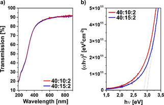
a) Transmission spectra and b) Tauc plots of the heterostructures with different In/Sn/Al oxide ratios of 40 : 10 : 2 and 40 : 15 : 2.
The Tauc plots for the two heterostructures of composition 40 : 10 : 2 and 40 : 15 : 2 (see Figure 3b) show only a marginal difference when the SnO2 content is increase from 10 to 15 layers. This is also evident from the calculated values of the optical bandgap, which are 2.88 eV and 2.99 eV for the stacks 40 : 10 : 2 and 40 : 15 : 2, respectively. A widening of the optical bandgap can be explained by an increased charge carrier density of the heterostructure with a higher amount of SnO2 (40 : 15 : 2) and is in accordance with the expected Burstein‐Moss shift.[34, 35]
In order to investigate the elemental composition and chemical states present within the metal oxide thin‐films, hard X‐ray photoelectron spectroscopy (HAXPES) was performed.[36] HAXPES delivers two advantages over conventional X‐ray photoelectron spectroscopy, which uses soft X‐ray excitation sources such as Al Kα. Firstly, the higher X‐ray energy leads to higher kinetic energies of the excited photoelectrons and therefore to a larger probing depth. The inelastic mean free path (IMFP) calculated using QUASES for the In 3d core level in In2O3 is 18.55 Å for Al Kα X‐rays (1.487 keV), whilst it increases by more than three times to 59.80 Å for the hard X‐ray energy of 5 keV used in this study.[37] This enables the study of multiple oxide layers across the thin‐film stack avoiding the necessity of destructive sputtering and the related artefacts to access buried layers. Secondly, using hard X‐rays deeper core levels can be accessed for many elements. In multi‐element systems, such as the thin‐film heterostructures explored here, overlap of core levels can complicate data analysis in standard XPS. For example, the low binding energy Al 2p core level overlaps with the much stronger In 4p core level, hindering analysis. Instead, hard X‐rays enable access to the much deeper Al 1s core level, which does not suffer any overlap and can therefore be used to examine its chemical state.[38] In the case of the samples investigated here, the core level spectrum for Al 2p would overlap with the one of In 4p while employing XPS.
Survey spectra for both heterostructures show all expected core lines (see Figure S3 and S4). In addition, small signals from adventitious C and the Si/SiO2 substrate are detected. The high‐resolution core level spectra for both samples, including Al 1s, O 1s, Sn 3d, and In 3d, are shown in Figure 4.
Figure 4.

HAXPES core level spectra of the In2O3/SnO2/Al2O3 multinary thin‐films of compositions 40 : 10 : 2 (blue) and 40 : 15 : 2 (red) for a) Al 1s, b) O 1s, c) Sn 3d, and d) In 3d. All spectra are normalized to the In 3d 5/2 peak height and are aligned to the Fermi level EF at 0 eV.
As discussed, the Al 1s core level was collected instead of the lower binding energy (BE) core levels to avoid spectral overlap (see Figure 4a). The core level has a BE of 1561.3 eV in good agreement with previous reports for Al2O3.[39] The O 1s core level spectra of the two thin‐films are dominated by a main peak with a BE of 530.8 eV, which can be assigned to metal oxide (M−O) environments (see Figure 4b). In addition, a clear shoulder on the higher BE side at ∼533 eV can be assigned to metal hydroxide (M−OH) species present on the surface and within the bulk of the thin‐film heterostructure.[20, 40] The difference in intensity between the peaks of the M−O and the M−OH species amounts to ∼72 % indicating that the majority of oxygen is present as metal oxide species. This finding can be attributed to the thermal post‐deposition treatment of the films, as residual hydroxyl groups, originating from the deposition process, are converted into fully coordinated oxygen at higher temperatures.[20, 41] Thus, the thermal post processing produces a high quality thin‐film primarily constituted of the oxides In2O3, SnO2, and Al2O3 and only to a minor extent of hydroxylated species. Comparing these results with those for ALD‐based IZO heterostructures, it can be concluded that by replacing ZnO with the combination SnO2/Al2O3, a significantly reduced amount of M−OH is obtained.[3] In previous work on IZO heterostructures, the influence of the ZnO amount in an IZO heterostack on the M−OH content via XPS was investigated. It was found that with increasing ZnO content the M−OH signal was systematically increased. This was verified by the investigation of the O 1s core level spectra of the single oxide.[3] In the current work, the small intensity difference of ∼3.7 % in the O 1s spectra attributed to the M−O peaks of the thin‐film compositions 40 : 10 : 2 and 40 : 15 : 2 results from the five additional layers for SnO2 in the latter film composition. The Sn 3d core level shows a clear intensity difference between the spectra of the two thin‐film compositions (see Figure 4c). The peaks of the heterostructure with 10 layers of SnO2 (40 : 10 : 2) show a ∼37 % lower intensity compared to the one with a higher SnO2 content. This decreased intensity of the 40 : 10 : 2 thin‐film is consistent with the compositional difference off 10 vs. 15 layers of SnO2. The core levels are located at 487.1 eV for Sn 3d 5/2 and 495.5 eV for Sn 3d 3/2, respectively, giving the expected spin orbital split (SOS) of 8.4 eV. These BEs are consistent with previously reported values for SnO2.[42] The core level spectra of In 3d (see Figure 4d)) are consistent with those reported for In2O3 and are positioned at 445.2 eV for In 3d 5/2 and 452.7 eV for In 3d 3/2, respectively, with a SOS of 7.5 eV.[40, 41]
In addition to core level spectra, HAXPES was also used to access the valence band (VB) region of the samples (see Figure 5a). The overall valence structure is dominated by In2O3 and agrees well with previous HAXPES data.[43] The clearly distinguishable feature at 8.9 eV stems from strong In 5 s and O 2p mixing, whilst the top of the VB is predominantly O 2p with some mixing with In 4d states. In between (5–8 eV) are states from intermixing of O 2p and In 5p orbitals. The relative intensities observed in the valence band are a direct reflection of the photoionization cross sections in HAXPES measurements with the In 5 s states being more dominant compared to the O 2p states, which dominate conventional soft X‐ray photoelectron spectroscopy.[44] The VB maximum (VBM) to Fermi energy EF separation can be determined from linear fits to the VBM (see Figure 5b). Only a small difference in the VBM‐EF separation is found with values of 3.2 eV and 3.1 eV for the thin‐films 40 : 10 : 2 and 40 : 15 : 2, respectively. This is in good agreement with the values found for lightly Sn‐doped In2O3,[45] and indicates that some intermixing of Sn and the In2O3 layer may occur in this heterostructure. Both samples also show a weak feature close to EF, terminating in a sharp Fermi edge at 0 eV (see magnified view in Figure 5c). This peak is associated with occupied In 5 s conduction band (CB) states.[44, 45] It increases in intensity with increasing carrier concentration, for example through Sn‐doping in In2O3. Some subtle differences are notable in the width and intensity of the feature, arising most likely from the difference in In : Sn ratio within the film stacks. However, the feature is too small and the differences too subtle to extract any quantitative conclusions.
Figure 5.

HAXPES valence band spectra, including a) valence band region, b) magnified region with linear fits intersecting the x‐axis and c) magnified region around the Fermi energy EF including filled conduction band states. EF in all subfigures denotes the position of the Fermi level located at 0 eV. The valence band region was normalized to the intensity of the In 3d 5/2 core level.
Thin‐film transistor performance of the ternary heteroatom stacks
The two heterostructure stacks In2O3/SnO2/Al2O3 of composition 40 : 10 : 2 and 40 : 15 : 2 were incorporated into TFT devices with a bottom‐gate‐bottom‐contact geometry, in order to assess the influence of the SnO2 layer thickness on the active semiconductor performance. The heterostructures were manufactured with an initial deposition of In2O3, followed by the deposition of SnO2 and Al2O3 and the iteration of the described supercycle to obtain the desired film thickness. Employing a highly conductive oxide to form the semiconductor‐dielectric interface has proven effective in realizing improved TFT performance. This improvement is attributed to an increased conductivity at the semiconductor‐dielectric interface, as well as an improved passivation of interfacial trap states.[3, 21] Electrical characterization of the fabricated transistors was performed in the form of current‐voltage (IV) measurements. The characteristic TFT parameters such as field‐effect mobility (μsat), threshold voltage (Vth), current on/off ratio (Ion/Ioff), and subthreshold swing (SS) were extracted from the transfer characteristics to allow comparison of heterostructures of different compositions (summarized in Table 1). Individual output and collective transfer characteristics, together with a schematic of the coated TFT device, are shown in Figure 6.
Table 1.
Comparison of the TFT performance parameters of the ternary heterostructures with different tin oxide compositions 40 : 10 : 2 and 40 : 15 : 2 in the dark and under irradiation with UV‐light (energy of 3.6 eV).
|
heterostructure In2O3/SnO2/Al2O3 |
mobility μsat [cm2 ⋅ V−1 s−1] |
on‐voltage Von [V] |
threshold‐voltage Vth [V] |
current on/off ratio IOn/IOff |
subthreshold swing SS [mV ⋅ dec−1] |
|||||
|---|---|---|---|---|---|---|---|---|---|---|
|
dark |
3.6 eV |
dark |
3.6 eV |
dark |
3.6 eV |
dark |
3.6 eV |
dark |
3.6 eV |
|
|
40 : 10 : 2 |
2.2 |
2.2 |
−0.1 |
−10.2 |
9.5 |
−0.3 |
2.6 ⋅ 108 |
1.2 ⋅ 106 |
328 |
823 |
|
40 : 15 : 2 |
2.0 |
2.0 |
−0.9 |
−8.8 |
8.6 |
−0.1 |
1.0 ⋅ 107 |
4.4 ⋅ 105 |
485 |
770 |
Figure 6.

Output characteristics of the ternary oxide heterostructure stacks of composition a) 40 : 10 : 2 and b) 40 : 15 : 2, and c) direct comparison of the transfer characteristics of the corresponding TFT devices. d) Schematic showing a cross‐section of a coated TFT substrate with bottom‐gate‐bottom‐contact geometry (not to scale) fabricated using ALD. The structure of the substrate with gate, dielectric, and source‐drain electrodes on a layer of ITO is shown. Depicted on top in red, blue and green is the layered structure of the single oxides with the sequence In2O3−SnO2−Al2O3 deposited in three individual supercycles.
The two investigated In2O3/SnO2/Al2O3 stacks (Figure 6c) differ only in the thickness of the intermediate SnO2 layer. In particular the thickness of the Al2O3 entity remains unchanged. The comparison of the two transistor compositions of ratios 40 : 10 : 2 and 40 : 15 : 2 shows that a higher tin content leads to a slightly decreased mobility as well as reduced IOn/IOff and a higher subthreshold swing (Table 1). Due to the increased tin oxide content in the 40 : 15 : 2 transistor composition, a higher density of free charge carriers is present in the active channel layer, which leads to an increased off‐current and an associated reduction of IOn/IOff. ALD‐based TFTs have been described which achieve mobility values of ∼4.5 cm2 ⋅ V−1 s−1, whose active semiconductor layer consists of aluminum zinc oxide, but also IZO TFTs that can reach values of up to 42 cm2 ⋅ V−1 s−1.[46] Polycrystalline In2O3/ZnO semiconductor layers obtained by ALD have been found to have mobilities ranging from 3.1 cm2 ⋅ V−1 s−1 up to 12.2 cm2 ⋅ V− s−1.[3] Compared to these, the composition 40 : 15 : 2 ranges in the lower region with a mobility of 2.0 cm2 ⋅ V−1 s−1. In addition to the mobility, the subthreshold swing (SS) is an important and indicative parameter of a TFT. It is related to the density of subgap states,[35] but also to the trap states at the interface between semiconducting and dielectric layer.[24] The oxide TFT with composition of 40 : 15 : 2 exhibits a subthreshold swing of 485 mV ⋅ dec−1. This value fits within the range for the previously mentioned polycrystalline In2O3/ZnO TFT, with reported SS values which range from 162 mV ⋅ dec−1 up to 621 mV ⋅ dec−1.[3]
TFTs using semiconducting heterostructures with the stacking sequence In2O3/SnO2/Al2O3, are unprecedented so far. Analogies to other systems, in which In2O3 is incorporated, such as In2O3/ZnO[3, 15] and ZTO/In2O3 [47] are evident, though. For further discussion it should also be mentioned that the addition of Al2O3 with near monolayer thickness is essentially required in order to achieve a semiconducting stack at all.[29] In contrast, individual In2O3, SnO2 layers, as well as binary In2O3/SnO2 films deposited by the employed ALD procedure exhibit conductive behavior. The Al2O3 layer is thus a very effective way to control oxygen vacancies in the SnO2 entity as well as interfacial traps.[29, 48]
For In2O3/ZnO bilayers it has been proposed that band bending occurs at the heterointerface due to electron migration from ZnO to In2O3 driven by the conduction bands offsets with the formed space charge resembling 2DEGs.[15] In an earlier investigation in our group, TFTs based on multilayers with repeated In2O3/ZnO units are synthesized by ALD.[3] Thereby the relative thickness of the individual layers of the heterostructure stacks directly affects the semiconducting performance. Higher amounts of defects are introduced by a higher thickness of the ZnO layers, while opposite to that thicker In2O3 layers resulted in higher mobilities (up to 12.2 cm2 ⋅ V−1 s−1). An increase in the In2O3 entity is, however, accompanied by unfavorable changes of other performance parameters (Ion/Ioff, SS, Vth). In an investigation by another group on inkjet‐printed ZTO/In2O3 bilayers, thinner In2O3 back channels result in an improvement of μsat, Ion/Ioff ratio as well as SS and Vth.[47] The overall performance can also be influenced merely by changes of constitution and microstructure. Diffusion effects have been found especially for SnO2 in heterostructures. Thus, a gradient of the Sn concentration is observed in SnO2/ZnO bilayers after processing.[49] Furthermore, a high interface roughness can be detrimental for the performance, which is a frequent problem in solution deposition.[29] In the herein presented work however, HRTEM indicates a clear layer structure and no obvious mixing is observed.
With respect to the electrical characterization and the parameters obtained, it can be concluded that the substitution of a semiconductor (ZnO), by a combination of a conductor and an insulator (SnO2/Al2O3), is a novel approach for fabricating active semiconducting materials for the application in TFT devices.
To determine the prevalent electron transport mechanism in the ternary thin‐films, the field‐effect mobility (μFE) is plotted logarithmically against the gate‐source voltage. By applying a power‐law fit [Eq. 1],
| (1) |
where VG , VT , and VP are the gate, threshold, and percolation voltages and K is a pre‐factor, the exponent γ is obtained, which provides information about the predominant transport mechanism.[50] Values for γ around 0.1 indicate a trap‐limited conduction (TLC), whereas values around 0.7 indicate a percolation conduction (PC).[3, 50] The dependency of the field‐effect mobility on the gate‐voltage for the discussed transistors is shown in Figure 7, while the respective values are summarized in Table 2.
Figure 7.

Dependence of the field‐effect mobility (μFE) on the gate‐source voltage (VGS) of the two transistors with different SnO2 contents. Shown in black are the corresponding power‐law fits by which the exponent γ is obtained.
Table 2.
Comparison of the exponent γ and the mobility values of the heterostructures with different SnO2 contents.
|
Transistor In2O3:SnO2:Al2O3 |
γ |
Mobility [cm2 ⋅ V−1 s−1] |
|---|---|---|
|
40 : 10 : 2 |
0.73 |
2.2 |
|
40 : 15 : 2 |
0.64 |
2.0 |
No noticeable difference is visible in the curves of the two transistors in the saturation regime starting at approximately VGS=10 V. Only the slope of the curves between VGS=0−7.5 V shows a slight difference.
Although the curves show strong similarities, there is a clear difference in the values obtained for γ. With an increased SnO2 content, the value decreases from 0.73 to 0.64. This value still indicates a TLC‐dominated transport mechanism, but the tin oxide content has a significant influence and can be attributed to an increased charge carrier density which raises the Fermi level. This allows some of the subgap states to be filled, acting no longer as trap states.
Assuming that the decrease in γ value with increasing SnO2 content follows a trend, a further increase in SnO2 layers would cause the conduction mechanism to shift towards the PC dominated regime. However, this would not be beneficial for gaining better device performance parameters, as an increasing SnO2 content also decrease the mobility values from 2.2 cm2 ⋅ V−1 s−1 to 2.0 cm2 ⋅ V−1 s−1 for the compositions 40 : 10 : 2 and 40 : 15 : 2, respectively.
To further investigate the effect of the tin oxide content on the properties of the semiconducting thin‐film, the behavior of the transistors and the associated changes in TFT performance parameters under illumination of various wavelength were examined. The devices were subjected to IV‐measurements while being illuminated with light of different wavelengths/energies.
The before mentioned In2O3/ZnO‐based TFTs show a decent light stability, as reflected by a shift of the transfer curves towards conductive behavior, an increase in off‐current, and a negative shift of the on‐voltage with increasing energy of illumination.[3] By replacing ZnO in the In2O3/ZnO semiconductor composition with a combination of the binary SnO2/Al2O3, a significantly improved stability against irradiation can be observed. This corresponds to a shift of the absorption in the heterostructure to slightly lower wavelengths, but is presumably also affected by an overall decrease in the carrier concentration.[51]
Comparison of the two TFTs shows a reduced increase in IOff and a smaller negative shift in Von for the transistor with a higher SnO2 content (Figure 8b). Figure 8 shows the alteration of the TFT transfer characteristics for semiconductor compositions of In2O3/SnO2/Al2O3 40 : 10 : 2 and 40 : 15 : 2 when illuminated with hν of different energies. An increase in conductivity is observed with increasing energy of irradiation. The increase in on‐current can be attributed to the generation of free charge carriers by irradiation with energy close to the bandgap of the heterostructure. This leads to the direct excitation of charge carriers into subgap states or to the release of charge carriers localized in trap states.[52] Comparison of the two TFTs shows a reduced increase in IOff and a smaller negative shift in Von for the transistor with a higher SnO2 content (Figure 8b). Even though the off‐current rises and the on‐voltage shift towards negative numbers with increasing energy of illumination, the transfer curves preserve their shape and show a semiconducting behavior even under intense UV illumination (Table 1).
Figure 8.

Transfer characteristics of the fabricated TFTs under illumination for the oxide heterostructures In2O3/SnO2/Al2O3 of composition a) 40 : 10 : 2 and b) 40 : 15 : 2.
An increase in off‐current and a negative shift in Von due to irradiation with light of increasing energy for both semiconductor compositions is observed (see Figure 8 and Table 1). This light‐induced instability can be explained by a persistent photo‐conductivity (PPC).[53] PPC is a phenomenon which can be observed in the increase in IOn and IOff with increasing energy of irradiation and thus decreasing IOn/IOff.
The reason for this is that the semiconducting channel has a high density of free charge carriers when it is in the switched‐on state. If further charge carriers are induced by irradiation, the conductivity of the transistor is only increased to a small extent. The photoconductivity can be observed more clearly in the switched‐off state of the transistor, in which the cannel is depleted of charge carriers. Irradiation induces charge carriers which increase the conductivity of the channel and thus leads to an increase in Ioff.[52] The shift in Von (and also Vth) with higher energies can be attributed to the photoinduced charge carriers, which can occupy a larger number of defects due to their higher energy. Filling of defects is necessary to achieve an appreciable electron flow at the interface between the individual metal oxide layers.[52] The ability of SnO2 to improve the overall trap density[23] is evident from the shift in Von. For the composition with a higher amount of SnO2 (40 : 15 : 2), this value is shifted by 7.9 V in the negative direction, while the value for the TFT with less SnO2 (40 : 10 : 2) experiences a larger negative shift of 10.1 V. Additionally, the shift in Von is attributed to the excitation of electrons from subgap states above the VBM into the conduction band.[35] During illumination with light of higher energies, the off‐current of the 40 : 10 : 2 TFT is raised by three orders of magnitude (Ioff,dark=1.0 ⋅ 10−11 A to Ioff,3.6eV=1.56 ⋅ 10−8 A), while Ioff of the 40 : 15 : 2 TFT, with an already high value under dark conditions (Ioff,dark=1.6 ⋅ 10−9 A), originating from the films higher conductivity, is raised by only one order of magnitude (Ioff,3.6eV=3.9 ⋅ 10−8 A). These two factors, a lower shift of Von and a lower increase of Ioff, indicate that an increased amount of SnO2 in the semiconducting layer leads to an improved stability under illumination for the respective transistor devices.
Conclusion
Thin‐film heterostructures of In2O3, SnO2, and Al2O3 were fabricated using ALD, employing trimethylindium, tetrakis‐(dimethylamino)tin, and trimethylaluminum as metal precursors and water as oxidant at a deposition temperature of 200 °C. By utilizing a layer‐by‐layer deposition process, the thin‐film composition can be controlled precisely. This provides a method to tune the properties of the resulting thin‐film transistors by accurately controlling the compositional changes within the semiconducting material. The thin‐films were found to be amorphous with a high optical transparency in the visible region. The thin‐film heterostructures were successfully integrated into TFT devices, which exhibit a saturation field‐effect mobility (μsat) of 2.0 cm2 V−1 s−1, a threshold voltage (Vth) of 8.6 V, a high current on/off ratio (IOn/IOff) of 1.0 ⋅ 107 and a low subthreshold swing (SS) of 485 mV dec−1. By using aluminum oxide as a component of the active semiconducting layer, an increased stability of the transistor performance against irradiation with light of different wavelengths, due to a broadening of the heterostructure's optical bandgap, was demonstrated. The improved stability is evident from a maintained semiconducting behavior of the transistor with a minor increase in off‐current (Ioff) of only one order of magnitude, even under intense UV illumination. The use of the ternary oxide composition In2O3/SnO2/Al2O3 demonstrates the possibility of creating active semiconducting layers based on the combination of conducting and insulating components, which can be utilized for the application in TFT devices. Future work could focus on the replacement of aluminum oxide in the active semiconducting layer. The incorporation of suitable oxides, which possess a rather large optical bandgap, but do not interfere with a convincing transistor performance, would certainly be worth investigating. The results presented herein give a general strategy towards developing ALD‐based heterostructure systems with optimized properties, especially their stability under illumination.
Experimental Section
Synthesis of the heteroatom stacks by ALD
The deposition of the heterostructure thin‐films In2O3/SnO2/Al2O3 was carried out using a Savannah S 100 System (Cambridge Ultratech). The metal precursors employed were trimethyl indium (TMI, Akzo Nobel), tetrakis(dimethylamino)tin (TDMASn),[54] and trimethyl aluminum (TMA, Strem Chemicals). Water (HPLC grade, Sigma‐Aldrich) was used as oxidant and argon (99.9999 %, Alpha Gaz™) as carrier gas. The depositions were performed at a base pressure of 1.5 Torr, a reactor temperature of 200 °C, and a carrier gas flow rate of 20 sccm. The precursors TMI and TMA, as well as the oxidant, were kept at room temperature, while TDMASn was heated to 60 °C. Before deposition the substrates were placed in the reactor and kept at 200 °C for 20 minutes under a constant argon flow of 20 sccm. For the deposition of the thin‐films, a recipe was developed in which the pulse duration, the exposure time, as well as the purge time were adapted to the respective precursor. The sequence used for In2O3 deposition was the following: TMI pulse of 0.1 s, exposition time of 1.5 s, argon purge of 20 s, H2O pulse of 0.1 s, exposition time of 1.5 s, and final argon purge of 20 s. For SnO2 the sequence was: TDMASn pulse of 0.5 s, exposition time of 1.5 s, argon purge of 30 s, H2O pulse of 0.015 s, exposition time of 1.5 s, and final argon purge of 30 s. For Al2O3 the following sequence was used: TMA pulse of 0.015 s, exposition time of 1.5 s, argon purge of 30 s, H2O pulse of 0.015 s, exposition time of 1.5 s, and final argon purge of 15 s. The compositional variation of the heterostructures was regulated by the number of layers deposited of each oxide. Here the number of layers for SnO2 were varied while those for In2O3 and Al2O3 were kept constant at 40 and 2, respectively. To obtain the desired film thickness the supercycle, consisting of the sequential deposition of the three single oxides, was repeated ten times.
Material characterization
UV‐vis measurements were performed on quartz substrates using an Evolution 600 spectrometer (Thermo Scientific) in a wavelength range of 190–900 nm. High resolution transmission electron microscopy (HRTEM) was performed on an FEI Tecnai G2 F20, with an operating voltage of 200 keV.[55] Samples used were coated TFT substrates (Fraunhofer IPMS, Dresden), annealed at 400 °C for 40 minutes and electrically characterized. Further processing included focused ion beam (FIB) preparation with an FEI Helios NanoLab 460F1 FIB‐SEM, followed by coating with a platinum layer.[56] Film thicknesses were obtained via ellipsometry using a spectroscopic ellipsometer M2000 (J. A. Woollam) in a spectral range of 370–1690 nm and an angular range of 45–85°. HAXPES measurements were performed at beamline P22 of PETRA III at the German Electron Synchrotron DESY in Hamburg, Germany.[57, 58] The data were collected at 5 keV with a defocused beam using Si (311) and attenuators (2+3+4) to reduce the photon flux by a factor of 10. Thus, an energy resolution of 130 meV could be achieved. A Phoibos 225HV analyzer (SPECS, Berlin, Germany) was used at an angle of 10° with respect to the sample surface. With the small area lens mode and a slit size of 3 mm, an excitation spot size of 0.1×0.1 mm2 was obtained, and a resolution of 203 meV was achieved.[57, 58] The obtained spectra were normalized to the In 3d 5/2 core level peak height and all spectra were aligned to the Fermi level.
Thin‐film transistor characterization
The multilayer semiconductor thin‐films were deposited on commercially available, prefabricated TFT substrates.[8, 59] These 15 mm×15 mm Substrates consist of highly n‐doped silicon with a 90 nm silicon dioxide dielectric layer. Source‐drain electrodes comprise of 40 nm gold with a 10 nm intermediate indium tin oxide (ITO) adhesion layer. The electrodes form an interdigital structure, with a channel length L=20 μm and width W=10 mm (W/L=500), in a bottom‐gate‐bottom‐contact (BGBC) geometry. Th TFT substrates, quartz slides (15 mm×15 mm) and Si/SiO2 substrates were cleaned sequentially with acetone, DI‐water and isopropanol (all HPLC‐Grade, Carl Roth GmbH & Co. KG) via ultrasonication for 10 minutes each and dried at 80 °C. Prior to deposition the substrates were treated with UV light (wavelength of 254 nm, optical power of 4 W) for 10 minutes, using a modified UV Ozone Cleaner UVC‐1014 (NanoBioAnalytics). Prior to electrical characterization of the transistors, all thin‐films were annealed at 400 °C for 40 minutes. The characterization was performed under the exclusion of white light in an inert gas atmosphere (argon) inside a glovebox, using a B1500A Semiconductor Device Analyzer (Agilent Technologies). The pressure inside the glovebox was constant at 2.7 mbar with a water content of <0.5 ppm and an oxygen content of <0.5 ppm. Light stability measurements were carried out using a switchable LED setup (Roithner Laser Technik GmbH), on which seven different wavelengths, from visible to UV range, can be selected. Illumination time for each wavelength was the time required for the measurement (10 Minutes). The charge carrier mobilities, μsat, as well as the threshold‐voltage Vth are obtained from a linear fit (see Figure S5) of the square root of the source‐drain current IDS 0.5 as a function of the gate‐source voltage VGS at 30 V, i. e. (ID,sat)0.5=(W*μsat*ci/2 L)0.5*(VGS−Vth), where ci refers to the capacity of the channel. This procedure assumes that the TFT is operated in saturation mode and the mobility does not depend on the applied gate voltage VGS, as in typical direct semiconductor, for example, silicon.
Conflict of interest
The authors declare no conflict of interest.
Supporting information
As a service to our authors and readers, this journal provides supporting information supplied by the authors. Such materials are peer reviewed and may be re‐organized for online delivery, but are not copy‐edited or typeset. Technical support issues arising from supporting information (other than missing files) should be addressed to the authors.
Supplementary
Acknowledgements
HRTEM investigations were performed at ERC Jülich, Germany, under contract ERC‐TUD1. We thank J. Engstler (TEM), S. Heinschke (ellipsometry) and J. Brötz (GIXRD), all at TUDa for measurements. J. J. S. acknowledges support through the DFG project SCHN375/36‐1. A. R. acknowledges the support from the Analytical Chemistry Trust Fund for her CAMS‐UK Fellowship. All authors acknowledge DESY (Hamburg, Germany), for beamtime at Beamline P22 under proposal I‐20190498. Funding for the HAXPES instrument by the Federal Ministry of Education and Research (BMBF) under contracts 05KS7UM1 and 05K10UMA with Universität Mainz; 05KS7WW3, 05K10WW1 and 05K13WW1 with Universität Würzburg is gratefully acknowledged. Open access funding enabled and organized by Projekt DEAL.
M. I. Büschges, R. C. Hoffmann, A. Regoutz, C. Schlueter, J. J. Schneider, Chem. Eur. J. 2021, 27, 9791.
Dedicated to Prof. Dr. Ulrich Schubert on the occasion of his 75th birthday
References
- 1.Wager J. F., Yeh B., Hoffman R. L., Keszler D. A., Curr. Opin. Solid State Mater. Sci. 2014, 18, 53–61. [Google Scholar]
- 2.Saarenpää H., Niemi T., Tukiainen A., Lemmetyinen H., Tkachenko N., Sol. Energy Mater. Sol. Cells. 2010, 94, 1379–1383. [Google Scholar]
- 3.Krausmann J., Sanctis S., Engstler J., Luysberg M., Bruns M., Schneider J. J., ACS Appl. Mater. Interfaces 2018, 10, 20661–20671. [DOI] [PubMed] [Google Scholar]
- 4.Kamiya T., Hiramatsu H., Nomura K., Hosono H., J. Electroceram. 2006, 17, 267–275. [Google Scholar]
- 5.Park J.-S., Kim T.-W., Stryakhilev D., Lee J.-S., An S.-G., Pyo Y.-S., Lee D.-B., Mo Y. G., Jin D.-U., Chung H. K., Appl. Phys. Lett. 2009, 95, 13503. [Google Scholar]
- 6.McDowell M. G., Sanderson R. J., Hill I. G., Appl. Phys. Lett. 2008, 92, 13502. [Google Scholar]
- 7.Wang D., Furuta M., Beilstein J. Nanotechnol. 2019, 10, 1125–1130. [DOI] [PMC free article] [PubMed] [Google Scholar]
- 8.Ahn C. H., Senthil K., Cho H. K., Lee S. Y., Sci. Rep. 2013, 3, 2737. [DOI] [PMC free article] [PubMed] [Google Scholar]
- 9.Park S.-H. K., Hwang C.-S., Ryu M., Yang S., Byun C., Shin J., Lee J.-I., Lee K., Oh M. S., Im S., Adv. Mater. 2009, 21, 678–682. [Google Scholar]
- 10.Fortunato E., Barquinha P., Goncalves G., Pereira L., Martins R., Solid-State Electron. 2008, 52, 443–448. [Google Scholar]
- 11.Chiang H. Q., Wager J. F., Hoffman R. L., Jeong J., Keszler D. A., Appl. Phys. Lett. 2005, 86, 13503. [Google Scholar]
- 12.Hosono H., J. Non-Cryst. Solids 2006, 352, 851–858. [Google Scholar]
- 13.
- 13a.Furuta M., Koretomo D., Magari Y., Aman S. M., Higashi R., Hamada S., Jpn. J. Appl. Phys. 2019, 58, 90604; [Google Scholar]
- 13b.Hong S., Park J. W., Kim H. J., Kim Y., Kim H. J., J. Inf. Disp. 2016, 17, 93–101. [Google Scholar]
- 14.
- 14a.Chen Z., Han D., Zhang X., Wang Y., Sci. Rep. 2019, 9, 1–13; [DOI] [PMC free article] [PubMed] [Google Scholar]
- 14b.Kim J.-I., Hwan Ji K., Yoon Jung H., Yeob Park S., Choi R., Jang M., Yang H., Kim D.-H., Bae J.-U., Dong Kim C., Appl. Phys. Lett. 2011, 99, 122102; [Google Scholar]
- 14c.Liu L., Chen S., Liang X., Pei Y., Adv. Electron. Mater. 2019, 5, 1900550. [Google Scholar]
- 15.Faber H., Das S., Lin Y.-H., Pliatsikas N., Zhao K., Kehagias T., Dimitrakopulos G., Amassian A., Patsalas P. A., Anthopoulos T. D., Sci. Adv. 2017, 3, e1602640. [DOI] [PMC free article] [PubMed] [Google Scholar]
- 16.Gassenbauer Y., Wachau A., Klein A., Phys. Chem. Chem. Phys. 2009, 11, 3049–3054. [DOI] [PubMed] [Google Scholar]
- 17.Yu X., Zhou N., Smith J., Lin H., Stallings K., Yu J., Marks T. J., Facchetti A., ACS Appl. Mater. Interfaces 2013, 5, 7983–7988. [DOI] [PubMed] [Google Scholar]
- 18.Macco B., Wu Y., Vanhemel D., Kessels W. M., Phys. Status Solidi RRL 2014, 8, 987–990. [Google Scholar]
- 19.
- 19a.Leskelä M., Ritala M., Angew. Chem. Int. Ed. 2003, 42, 5548–5554; [DOI] [PubMed] [Google Scholar]; Angew. Chem. 2003, 115, 5706–5713; [Google Scholar]
- 19b.Nilsen O., Balasundaraprabhu R., Monakhov E. V., Muthukumarasamy N., Fjellvåg H., Svensson B. G., Thin Solid Films 2009, 517, 6320–6322; [Google Scholar]
- 19c.Ritala M., Leskelä M., Dekker J.-P., Mutsaers C., Soininen P. J., Skarp J., Chem. Vap. Deposition 1999, 5, 7–9. [Google Scholar]
- 20.Sanctis S., Krausmann J., Guhl C., Schneider J. J., J. Mater. Chem. C 2018, 6, 464–472. [Google Scholar]
- 21.Liu G. X., Liu A., Shan F. K., Meng Y., Shin B. C., Fortunato E., Martins R., Appl. Phys. Lett. 2014, 105, 113509. [Google Scholar]
- 22.Kamiya T., Hosono H., NPG Asia Mater. 2010, 2, 15–22. [Google Scholar]
- 23.Ryu M. K., Yang S., Park S.-H. K., Hwang C.-S., Jeong J. K., Appl. Phys. Lett. 2009, 95, 72104. [Google Scholar]
- 24.Jaehnike F., Pham D. V., Bock C., Kunze U., J. Mater. Chem. C 2019, 7, 7627–7635. [Google Scholar]
- 25.Fortunato E., Barquinha P., Martins R., Adv. Mater. 2012, 24, 2945–2986. [DOI] [PubMed] [Google Scholar]
- 26.Grover M. S., Hersh P. A., Chiang H. Q., Kettenring E. S., Wager J. F., Keszler D., J. Phys. D 2007, 40, 1335. [Google Scholar]
- 27.Cho D.-H., Yang S., Byun C., Ryu M. K., Park S.-H. K., Hwang C.-S., Yoon S. M., Chu H.-Y., IEEE Electron Device Lett. 2008, 30, 48–50. [Google Scholar]
- 28.Allemang C. R., Cho T. H., Trejo O., Ravan S., Rodríguez R. E., Dasgupta N. P., Peterson R. L., Adv. Electron. Mater. 2020, 6, 2000195. [Google Scholar]
- 29.Park H., Choi H., Lee N., Jung C., Choi Y., Song S., Choi Y., Kim K., Kim J., Lee J., Ceram. Int. 2020, 46, 12782–12787. [Google Scholar]
- 30.Jeong J. K., Yang S., Cho D.-H., Park S.-H. K., Hwang C.-S., Cho K. I., Appl. Phys. Lett. 2009, 95, 123505. [Google Scholar]
- 31.
- 31a.Tanner C. M., Perng Y.-C., Frewin C., Saddow S. E., Chang J. P., Appl. Phys. Lett. 2007, 91, 203510; [Google Scholar]
- 31b.Jang K., Park H., Jung S., van Duy N., Kim Y., Cho J., Choi H., Kwon T., Lee W., Gong D., Thin Solid Films 2010, 518, 2808–2811. [Google Scholar]
- 32.
- 32a.Lee D.-J., Kwon J.-Y., Lee J. I., Kim K.-B., J. Phys. Chem. C 2011, 115, 15384–15389; [Google Scholar]
- 32b.Ott A. W., Klaus J. W., Johnson J. M., George S. M., Thin Solid Films 1997, 292, 135–144; [Google Scholar]
- 32c.Mullings M. N., Hägglund C., Bent S. F., J. Vac. Sci. Technol. A 2013, 31, 61503. [Google Scholar]
- 33.Lee D.-J., Kwon J.-Y., Kim J., Kim K.-J., Cho Y.-H., Cho S.-Y., Kim S.-H., Xu J., Kim K.-B., J. Phys. Chem. C 2014, 118, 408–415. [Google Scholar]
- 34.Antony A., Nisha M., Manoj R., Jayaraj M. K., Appl. Surf. Sci. 2004, 225, 294–301. [Google Scholar]
- 35.Kamiya T., Nomura K., Hosono H., Sci. Technol. Adv. Mater. 2010, 11, 44305. [DOI] [PMC free article] [PubMed] [Google Scholar]
- 36.Kalha C., Fernando N. K., Bhatt P., Johansson F., Linblad A., Rensmo H., Mendina L. Z., Lindblad R., Siol S., Jeurgens L., J. Phys. Condens. Matter 2021, 33, 233001. [DOI] [PubMed] [Google Scholar]
- 37.Tanuma S., Powell C. J., Penn D. R., Surf. Interface Anal. 1994, 21, 165–176. [Google Scholar]
- 38.Siol S., Mann J., Newman J., Miyayama T., Watanabe K., Schmutz P., Cancellieri C., Jeurgens L. P. H., Surf. Interface Anal. 2020, 52, 802–810. [Google Scholar]
- 39.
- 39a.Regoutz A., Mascheck M., Wiell T., Eriksson S. K., Liljenberg C., Tetzner K., Williamson B. A. D., Scanlon D. O., Palmgren P., Rev. Sci. Instrum. 2018, 89, 73105; [DOI] [PubMed] [Google Scholar]
- 39b.Nishida S., Yasunaga S., Otomo S., Sasaki H., J. Surf. Anal. 2019, 26, 216–217. [Google Scholar]
- 40.Tetzner K., Isakov I., Regoutz A., Payne D. J., Anthopoulos T. D., J. Mater. Chem. C 2017, 5, 59–64. [Google Scholar]
- 41.Socratous J., Banger K. K., Vaynzof Y., Sadhanala A., Brown A. D., Sepe A., Steiner U., Sirringhaus H., Adv. Funct. Mater. 2015, 25, 1873–1885. [DOI] [PMC free article] [PubMed] [Google Scholar]
- 42.Borgatti F., Berger J. A., Céolin D., Zhou J. S., Kas J. J., Guzzo M., McConville C. F., Offi F., Panaccione G., Regoutz A., Phys. Rev. B 2018, 97, 155102. [Google Scholar]
- 43.Davies D. W., Walsh A., Mudd J. J., McConville C. F., Regoutz A., Kahk J. M., Payne D. J., Dhanak V. R., Hesp D., Pussi K., J. Phys. Chem. C 2018, 123, 1700–1709. [Google Scholar]
- 44.Körber C., Krishnakumar V., Klein A., Panaccione G., Torelli P., Walsh A., Da Silva J. L., Wei S.-H., Egdell R. G., Payne D. J., Phys. Rev. B 2010, 81, 165207. [DOI] [PubMed] [Google Scholar]
- 45.Walsh A., Da Silva J. L. F., Wei S.-H., Körber C., Klein A., Piper L. F., DeMasi A., Smith K. E., Panaccione G., Torelli P., Phys. Rev. Lett. 2008, 100, 167402. [DOI] [PubMed] [Google Scholar]
- 46.Sheng J., Lee H.-J., Oh S., Park J.-S., ACS Appl. Mater. Interfaces 2016, 8, 33821–33828. [DOI] [PubMed] [Google Scholar]
- 47.Lee S.-H., Choi W.-S., J. Disp. Technol. 2015, 11, 698–702. [Google Scholar]
- 48.Cho S. W., Kim K. S., Jung S. H., Cho H. K., J. Mater. Chem. C 2017, 5, 10498–10508. [Google Scholar]
- 49.Nam S., Yang J.-H., Cho S. H., Choi J. H., Kwon O.-S., Park E.-S., Lee S.-J., Cho K.-I., Jang J., Hwang C.-S., J. Mater. Chem. C 2016, 4, 11298–11304. [Google Scholar]
- 50.Lee S., Ghaffarzadeh K., Nathan A., Robertson J., Jeon S., Kim C., Song I.-H., Chung U.-I., Appl. Phys. Lett. 2011, 98, 203508. [Google Scholar]
- 51.Gao Y., Lu J., Zhang J., Li X., RSC Adv. 2015, 5, 37635–37639. [Google Scholar]
- 52.Barquinha P., Pimentel A., Marques A., Pereira L., Martins R., Fortunato E., J. Non-Cryst. Solids 2006, 352, 1756–1760. [Google Scholar]
- 53.Ide K., Nomura K., Hosono H., Kamiya T., Phys. Status Solidi A 2019, 216, 1800372. [Google Scholar]
- 54.Jones K., Lappert M. F., J. Chem. Soc. 1965, 1944–1951. [Google Scholar]
- 55.Luysberg M., Heggen M., Tillmann K., JLSRF 2016, 2, 77. [Google Scholar]
- 56.Kruth M., Meertens D., Tillmann K., JLSRF 2016, 2, 59. [Google Scholar]
- 57.Schlueter C., Gloskovskii A., Ederer K., Schostak I., Piec S., Sarkar I., Matveyev Y., Lömker P., Sing M., Claessen R. (Eds.) The new dedicated HAXPES beamline P22 at PETRAIII, AIP Publishing LLC, 2019. [Google Scholar]
- 58.Drube W., Hloskovsky A., Sarkar I., Piec S., Schulz-Ritter H., Okrent F., Claessen R., Schoenhense G., Schneider C., Wiemann C. (Eds.) PETRA III Extention Project. X-ray spectroscopy beamline P22 HAXPES / HAXPEEM. Technical Design Report, AIP Publishing LLC, 2016. [Google Scholar]
- 59.Fraunhofer IPMS, End-of-Line Standard Substrates for the Characterization of Organic Semiconductor Materials: OFET-Structures on Silicon with Au Source/Drain and 90 nm SiO2 Gate-Insulator Generation 4.
Associated Data
This section collects any data citations, data availability statements, or supplementary materials included in this article.
Supplementary Materials
As a service to our authors and readers, this journal provides supporting information supplied by the authors. Such materials are peer reviewed and may be re‐organized for online delivery, but are not copy‐edited or typeset. Technical support issues arising from supporting information (other than missing files) should be addressed to the authors.
Supplementary