Abstract
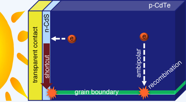
In some thin-film solar cells the light-absorbing layer is a mosaic of crystalline grains whose boundaries run from the back to the front of the cell. We used the semiconductor modeling software Sesame to do numerical calculations of the optoelectronic properties of such cells assuming that recombination of minority photocarriers occurs primarily at the grain boundaries. The work complements analytical results for diffusion-limited recombination at grain boundaries and dislocations. We chose idealized n-CdS/p-CdTe solar cells for illustration. We find that the open-circuit voltage, VOC, under illumination declines logarithmically with increasing ratio D/θ2, where D is the ambipolar diffusion constant governing minority-carrier transport and θ is the grain size (from 1 to 10 μm). While a decline in VOC as mobility increases is counterintuitive, this finding is consistent with related analytical results and confirms their utility. However, open-circuit voltages are about 0.04–0.10 V lower than the corresponding analytical estimates. We show that the deficit is mostly a consequence of a recombination shortcut. At open circuit, minority photocarrier currents at points closer to the n-CdS interface than to a grain boundary are directed through the conducting front layers and terminate near the “hot spot” at the intersection with the grain boundary. The shortcut lowers open-circuit voltages by about 0.05 V below the analytical estimates.
Keywords: diffusion-limited recombination, polycrystalline thin-film solar cells, CdTe, grain boundary, minority carrier mobility
I. Introduction
In polycrystalline semiconductors, minority photocarriers may recombine primarily at the grain boundaries. Within a grain, photocarriers generated at different locations have individual lifetimes determined by their initial distance from the grain boundary and by the ambipolar diffusion coefficient D. Computationally, the simplest case is a laminar stack of platelike grains with boundaries perpendicular to the cell’s surface. For plates of width θ with large grain boundary recombination velocities S ≫ D/θ, an analytical calculation for uniform photogeneration yields an average minority carrier recombination lifetime τ = θ2/12D.1 For cylindrical grains of diameter θ the lifetime is θ2/32D (see the Appendix). The results assume ambipolar diffusion of minority carriers and apply when the grains are not strongly depleted by charge exchange with the grain boundaries. We will discuss the other case of strong depletion in section IV. This type of “diffusion-limited” recombination model has also been formulated for dislocations threading up through a crystal.2 Photovoltaic cells to which analytical diffusion-limited recombination models have been applied include thin-film silicon,3−6 gallium nitride,7 halide-based perovskites,8 and complex organic and nanoporous materials.9,10 It is implicit in these models that the average photocarrier recombination lifetime τ is inversely proportional to the ambipolar diffusion coefficient and, thus, usually to the minority carrier mobility μmin.11 For the grain boundary limited lifetime just noted, no additional microscopic details of the grain boundary need to appear in the calculation.
Analytical calculations of average lifetimes are obviously useful when extended defects such as dislocations are spaced finely compared to the other relevant length scales such as the median absorption length for solar photons. For crystalline silicon, the absorption length is hundreds of micrometers.12 For an areal density of dislocations greater than 1010 m–2, the mean distance from a point of photogeneration to a dislocation is less than 10 μm. In such “fine-grained” materials, modeling can plausibly be done by using a one-dimensional (1D) model and the minority carrier lifetime, τ, averaged over the photogeneration profile. Thus, for uniform photogeneration and ideal contact layers, the open-circuit voltage (for a p-type material) is4
| 1 |
where Efn is defined as the mean electron quasi-Fermi level in a grain calculated from the average electron lifetime and the photogeneration rate G. Efp is the hole quasi-Fermi level calculated from the acceptor concentration, NA, and neglecting the density of photogenerated holes, p. ni is the intrinsic dark carrier density of the semiconductor at temperature T, e is the electron charge magnitude, and kT is the thermal energy. For average lifetimes determined by grain boundaries, we recast eq 1 using the simplest form for grain boundary recombination with laminar grains of width θ:
| 2a |
| 2b |
Here we assumed that the ambipolar diffusion coefficient is determined by the minority carrier mobility, μmin, and the Einstein relation: D = (kT/e)μmin. Note that increasing the minority carrier mobility decreases the open-circuit voltage; in effect, a low ambipolar diffusion coefficient “insulates” the semiconductor bulk from the grain boundaries.
In the present work, the question we ask is how well the insights from 1D models using averaged, diffusion-limited lifetimes apply to two-dimensional (2D) models of polycrystalline mosaic solar cells; we use the term “mosaic” to describe polycrystalline structures where the grain boundaries primarily run perpendicular to the surface of the cell. We chose thin-film CdTe solar cells for illustration. The champion efficiency thin-film CdTe cells have an open-circuit voltage, VOC, under solar illumination of 0.876 V at 298 K.13 This value is substantially smaller when compared with recent values in single crystal CdTe solar cells, where VOC has now reached 1.096 V.14,15 The reduced value is plausibly attributable to grain boundary recombination.
For our numerical calculations, we used Sesame, a semiconductor modeling software developed to solve the drift-diffusion-Poisson equations in multidimensions.16 The material parameters are summarized in Table 1. The parameters are similar to previous modeling of large grain CdS/CdTe solar cells17−23 but were selected to avoid substantial charge depletion of the grains by the grain boundaries.
Table 1. List of Parameters Used in the Numerical Simulations.
| parameters | CdS | CdTe |
|---|---|---|
| thickness x (nm) | 10 | 3000 |
| grain size θ (nm) | 103–104 | |
| energy gap Eg (eV) | 2.4 | 1.5 |
| electron affinity χ (eV) | 4.38 | 4.28 |
| dielectric constant ε | 8.4 | 10.2 |
| acceptor concentration NA (cm–3) | 0 | 1.0 × 10¹⁵ |
| donor concentration ND (cm–3) | 1.0 × 10¹⁷ | 0 |
| electron mobility μe (cm2/(V s)) | 160 | 9–1000 |
| electron lifetime τe (ns) | 0.1 | see LD |
| hole mobility μh (cm2/(V s)) | 15 | 80 |
| hole lifetime τe (ns) | 10–3 | see LD |
| ambipolar diffusion length LD (cm)34 | >θ |
| CdTe grain boundary parameters | |
|---|---|
| defect type | donor (D) |
| defect density per area Ngb (cm–2) | 1.0 × 10¹⁰ |
| defect energy level Et (eV) | 0.75 eV below ECa |
| capture cross section for electrons σe (cm2) | 1.0 × 10⁻¹¹ |
| capture cross section for holes σh (cm2) | 1.0 × 10⁻¹² |
EC denotes the energy of the conduction band minimum.
The symbols in the upper panel of Figure 1 show the dependence of the numerical calculations of VOC upon the ratio μe/θ2, where electrons are assumed to be the minority carrier and μe is their mobility. The calculations are done under standard AM 1.5G 1-sun illumination conditions (100 mW/cm2) at 300 K. The solid line labeled “analytical” is derived from eq 2b and assumes uniform photogeneration (G = 6.3 × 1020 cm–3 s–1) yielding the same short-circuit current density, JSC, as for solar illumination conditions. The numerical and analytical results have essentially the same dependence on μe/θ2. As we discuss subsequently, the decrease of about 0.05 V between the analytical and numerical results is not primarily due to the difference in solar and uniform photogeneration profiles. It is mostly due to a minority photocarrier shortcut to recombination through the CdS emitter and the front contact layers; the actual recombination event is near the intersection of a grain boundary and the CdS layer. We call this recombination region near the intersection a “hot spot”. Such hot spots were noted by Gaury and Haney in CdTe cell simulations24 and in much earlier work in polycrystalline silicon.25
Figure 1.
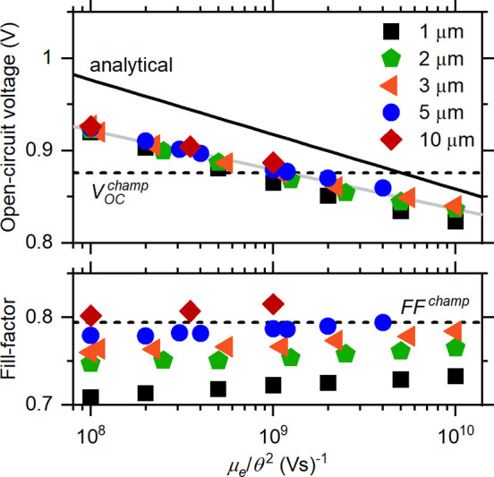
Symbols indicate numerical calculations for the open-circuit voltages VOC (upper panel) and the fill factors FF (lower panel) for CdS/CdTe solar cells under solar illumination at 300 K. The horizontal axis is the ratio of electron carrier mobility μe and the square of grain size θ as given in the key. Note the linear dependence of the VOC upon the μe/θ2 ratio as guided by the solid gray line. The solid line represents the analytical solution given by eq 2b with uniform photogeneration G = 6.3 × 1020 cm–3 s–1. The dashed lines are guides for the eye and indicate the open-circuit voltage VOCchamp and the fill factor FFchamp for the champion CdTe thin-film solar cell at 298 K.13
The numerical calculations of the fill factors FF for the cells have a quite different dependence on the electron carrier mobility, μe, and grain size, θ. To our knowledge, there have not been related analytical calculations. There is only a slight increase in FF with μe, which contrasts with the decrease in VOC. We think this is because of the very small depth of solar photogeneration in CdTe (∼0.3 μm), which avoids photoinduced space-charge effects.26 The noticeable increase in FF with grain size is a second consequence of the shortcut to the recombination hot spot. The effect is qualitatively similar to interface recombination at the CdS/CdTe interface but intrinsically varies with grain boundary properties.
For reference, we also show the values of the open-circuit voltage, VOCchamp, and the fill factor, FFchamp, for the present champion thin-film CdTe solar cell (see dashed lines in Figure 1).13 The champion open-circuit voltage, VOC, corresponds to μe/θ2 = 109 V–1 s–1. To achieve the single-crystal cell VOC ≈ 1.10 V in a polycrystalline cell would require μe/θ2 = 104 V–1 s–1, which would correspond to grain sizes of hundreds of micrometers. At the same time, the ambipolar diffusion length, LD, within a grain would need to be larger than the grain size, θ—otherwise, the bulk recombination of the intragrain material would limit the open-circuit voltage, which would become independent of the grain size. A simulation for 100 μm grains, an electron carrier mobility of 100 cm2/(V s), and a correspondingly enormous recombination time (τ = 2 × 10⁻⁴ s) gave a VOC = 1.02 V, which is on the (solid gray) trend line of Figure 1.
The trade-off of the electron carrier mobility and the grain size does not apply to the cell fill factor, which increases mostly with grain size, θ. Note, a grain size θ = 5 μm gave a fill factor as large as the champion cell. We note that the analytical calculations presented in the Appendix show that laminar grains lead to VOC values about 0.02 V higher than for cylindrical grains. Cylindrical grains would arguably be a better approximation to actual polycrystalline mosaic cells than laminar grains.
In the following, we first present the details of the numerical solar cell calculations summarized in Figure 1. We then show the complex contour plots of photocarrier densities and currents from the simulations. Inspecting these plots, it is not obvious why the analytical average lifetime approach is a useful guide to VOC. It turns out that much of this complexity is associated with the intersection of a grain boundary and the front, n-type CdS layer. As noted earlier, near the intersection, there is a recombination hot spot that is not envisioned in the analytical calculations. Here, we show that electrons generated near the CdS/CdTe interface, but relatively distant from the grain boundary, induce an Ohmic current of electrons in the CdS and the front contact layers that terminates at the hot spot. We identify this recombination shortcut as a channel that lowers the open-circuit voltage. A minority photocarrier at a particular point in the CdTe that is closer to the CdS than to the grain boundary needs to diffuse only the shorter distance before merging into a high conductivity highway to the hot spot. As we illustrate in section III, this recombination shortcut lowers VOC by about 0.05 V. This recombination channel would mimic true interface recombination in experiments and possibly account for the improvement in fill factors with grain size in Figure 1.
II. Simulation Details
The numerical simulations were performed by using the two-dimensional (2D) semiconductor modeling software Sesame to solve the electron and hole continuity equations simultaneous with the Poisson equation.16 The script calculates the properties of a pn+ junction solar cell with a polycrystalline array of grains with planar grain boundaries. For orientation, in Figure 2 we show the contour map of the hole density calculated under dark conditions at 0 V for the CdS/CdTe solar cell model system. A single planar grain boundary is positioned in the middle of the CdTe absorber, perpendicular to the junction between CdS and CdTe layers, and terminates at 0.05 μm from the p-type (right) contact. The grain boundary extends indefinitely down into and up out of the page. The grain width is θ = 3 μm, which is also the thickness of the p-type CdTe absorber layer. The model assumes that the incident light enters through the front n-type CdS emitter (window) layer, the thin green layer at the left in Figure 2. The solar photogeneration profile is calculated by using Sesame’s built-in table for the 1-sun terrestrial illumination (100 mW/cm2 AM1.5G) spectrum27 and those for the absorption spectra of CdS and CdTe layers.28,29 The numerical integration of the resulting generation rate profile, G(x), yielded a short-circuit density current of about 28.5 mA/cm2. As other workers have noted, the champion cell’s short-circuit current is about 2 mA/cm2 larger than can be explained by optical absorption measurements on CdTe;20,30 the short-circuit current density JSC reported for the champion cell was 30.25 mA/cm2.13 We assumed selective Ohmic contacts such that electron current vanishes at x = L (right contact) and the hole current vanishes at x = 0 (left contact).
Figure 2.
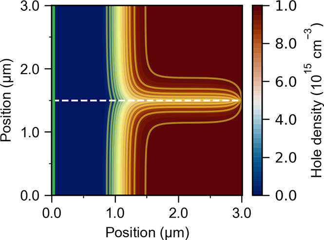
Contour plot for the hole density of the CdS/CdTe cell with a single planar grain boundary (dashed line) perpendicular to the junction, under short-circuit conditions in the dark. The thin green layer indicates the 10 nm thick n-type CdS emitter layer. The built-in potential is VBI = 1.08 V, the acceptor concentration is NA = 1.00 × 1015 cm–3, and the grain-boundary donor density is Ngb = 1.00 × 1010 cm–2. The thickness of the depletion layer near the CdS layer and that of the depletion region of the grain boundary (solid yellow contour lines) agree with elementary calculations.
The assumption of a laminar array of grains is computationally and analytically convenient; however, it is a rough approximation for a mosaic of columnar grains. The corresponding analytical model noted earlier yields an average steady-state recombination lifetime for photocarriers in a grain of τ = θ2/12D with large grain boundary recombination velocities. In the Appendix, we show that a cylindrical grain geometry yield τ = θ2/32D. The laminar approximation for VOC is then larger than for the cylindrical geometry by (kBT/e) ln(8/3) = 0.026 V.
The acceptor concentration of the CdTe layer was set to NA = 1015 cm–3. This value is in the range of previous modeling of CdTe solar cells and is large enough that the photogenerated density of minority carriers remained smaller than NA.20,24,31 We assumed the planar grain boundary has a donor density Ngb = 1010 cm–2. This small donor density was chosen to clarify comparison with the diffusion-limited model even for 1 μm grains. Generally, we expect the model to apply when the grain boundary depletion width is much smaller than the grain width θ. Our assumptions for the grain boundary parameters correspond to a very thin depletion layer (0.1 μm) extending into the CdTe layer. The depletion regions to the right of the CdS interface and above and below the grain boundary are evident in Figure 2.
In Table 1, we present the primary parameters used in the simulations; some additional parameters normally used for CdTe and CdS are given in an endnote.32 We varied the minority carrier (electron) mobility μe widely, from 9 to 1000 cm2/(V s). The bulk ambipolar diffusion length of the photocarriers, LD, in the p-type CdTe layer was kept larger than the width of the grains, such that the calculations were focused on recombination at the grain boundaries. The grain boundary recombination velocity for electrons S = Ngbσevth was set to be 106 cm/s, which is near the upper range of experimental estimates in p-type CdTe and previous modeling studies,17,33 where vth = 107 cm/s is the thermal velocity and σe is the capture cross section for electrons. This corresponds to a fairly large electron capture cross section, σe = 1.0 × 1011 cm2. The full analytical formula for the effective recombination lifetime of a polycrystalline bulk material with diffusion-limited recombination at planar surfaces is1
| 3 |
The diffusion and recombination velocity terms are comparable only at the extremes of our simulations (θ = 10–4 cm, D = 25 cm2/s). If the recombination velocity is small and its term in eq 3 is larger than the diffusion term, the minority photocarrier density will vary little within a grain, and the ambipolar diffusion coefficient (and hence the minority carrier mobility) will not affect the average lifetime or the open-circuit voltage. Given the presumption of a large grain boundary recombination velocity and neglecting true interface recombination at the CdS/CdTe interface, only three materials quality parameters significantly affected the simulations: the CdTe acceptor concentration NA, the grain size θ, and the electron mobility μe. The numerical simulation was relatively insensitive to most of the other parameters: the density of grain boundary donors ND, the electron capture cross sections σe, the hole capture cross section σh, the majority (hole) carrier mobility μh, and the bulk ambipolar diffusion length LD (as long as it is larger than θ).
III. Dependence of VOC on the Ratio μe/θ2
We return to the dependence of the open-circuit voltage upon the ratio μe/θ2. A material with a perfect junction and perfect contacts, under uniform photogeneration, G, and sufficiently large grain-boundary recombination velocity should obey eq 2 for its implied open-circuit voltage, VOC. In Figure 3, we graph this analytical calculation (solid black line) along with the numerical calculations for both solar illumination and uniform photogeneration with the same absorbed photon flux (G = 6.3 × 1020 cm–3 s–1) in the CdTe layer. The solid symbols are calculated with a grain boundary that runs from 0.05 μm above the p-type back contact to the CdS/CdTe interface. The open symbols are a simulation in which the grain boundary ends 0.4 μm below the CdS/CdTe interface.
Figure 3.
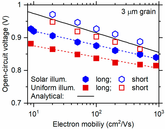
Analytical and numerical estimates of the open-circuit voltage, VOC, for cells with θ = 3 μm thick grains and varying electron carrier mobilities, μe. The blue (open and solid) symbols indicate VOC under solar illumination. The red (open and solid) symbols and the “analytical” line are obtained with uniform photogeneration (G = 6.3 × 1020 cm–3 s–1). The open symbols are results obtained with a shortened grain boundary that stops 0.4 μm before the CdS/CdTe interface. The dashed red and blue lines are guides only.
It is unsurprising that the numerical calculations with solar illumination give larger values for VOC than with uniform photogeneration. The solar photogeneration profile in CdTe absorber layer is strongly peaked near the CdS interface, and the electron quasi-Fermi level near that interface determines VOC.26,35 With the full-length grain boundary, there is a deficit of around 0.05 V between the analytical and numerical calculations with uniform photogeneration. As we shall illustrate shortly, this deficit is mostly due to the recombination shortcut for electrons which terminates at the intersection of the grain boundary and the CdS/CdTe interface. When the grain boundary terminates short of the interface, there is good agreement between the analytical and numerical calculations.
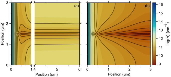
We explore the numerical calculations further in Figure 4, which uses μe = 100 cm2/(V s) and a full-length grain boundary. Figure 4a shows the electron density contours for a very thick cell (x = 6 μm) and uniform photogeneration. Deep in the CdTe layer, the contours correspond well to the diffusion-limited, analytical calculation. The maximum electron density is in a plane separated by 1.5 μm from the grain boundary planes; the density declines parabolically to near zero at the grain boundary. Near the CdS/CdTe interface, the contours are complex as they go from perpendicular to parallel to the interface. Given the complexity, it is remarkable that the analytical scaling of VOC with −(kT/e) ln(μe/θ2) still applies fairly well. Figure 4b shows the electron density contours with solar illumination for a 3 μm cell. The complexity of the electron density contours increases further because the photogeneration is close to the CdS interface instead of being spread uniformly through the cell. As presented in Figure 3, solar illumination increases VOC from 0.84 to 0.88 V, and its scaling with −(kT/e) ln(μe/θ2) has the same trend as with uniform photogeneration.
Figure 4.
Numerical calculations of the electron density contour maps at open-circuit voltage for (a) a 6 μm thick cell under uniform photogeneration (G = 6.3 × 1020 cm–3 s–1) and (b) a 3 μm thick cell under solar illumination containing a single grain boundary intersecting the n-type CdS layer (at the left edge) at its center. The solid (dark gray) lines are guides for the reader’s eye and illustrate the electron density contours. The grain boundary contains a single donor with a defect density Ngb = 1010 cm–2 and a recombination velocity S = 106 cm/s and is located at 0.85 eV (for uniform photogeneration) and at 0.75 eV (for solar illumination) below the conduction band edge, respectively. All calculations are done for μe = 100 cm2/(V s) and μh = 80 cm2/(V s); the simulation parameters are given in Table 1.
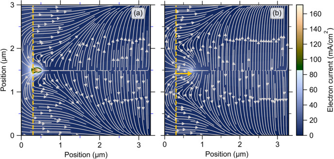
One physical reason for why the analytical result of eq 1 does not give a precise account for the magnitude of VOC in cells with uniform photogeneration proves to be simple. In Figure 5a, we show a map of calculated electron currents at open-circuit conditions and with uniform photogeneration. For illustration only, we made the CdS layer 0.3 μm thick. Electrons near the back of the cell flow in the expected pattern toward the planar grain boundary and recombination. On the other hand, electrons closer to the front CdS interface flow first into the highly conducting CdS. As illustrated in Figure 5a, the electron current continues through the CdS and front contact. It finally delivers electrons to the hot spot where they recombine with holes. Once a photogenerated electron reaches the CdS layer, the distant recombination event at the hot spot occurs nearly instantaneously due to dielectric relaxation processes. We refer to this recombination channel as the “shortcut” channel. This effect is further illustrated in Figure 5b, where the grain boundary was terminated about 0.4 μm from the CdS interface. The shortening of the grain reduces the effect of the shortcut channel. Electron currents from the CdS to the hot spot now need to surmount the barrier presented by the depletion region to reach the hot spot. The hot spot is noticeably cooler, and Voc increased, as shown in Figure 3.
Figure 5.
Electrical current flows of electrons at open circuit with uniform photogeneration (G = 6.3 × 1020 cm–3 s–1) for two types of grain boundary lengths: (a) a full-length grain terminated at the CdS interface and (b) a shorter grain terminated 0.4 μm before it reached the CdS layer interface; the orange arrow indicates the position at which the grain boundary terminates. The dashed orange lines mark the CdS/CdTe interface. The CdS layer thickness was increased to 0.3 μm for a better illustration of the electron current flow. The gray arrows indicate the direction of the electron flow. The numerical calculations are done for μe = 100 cm2/(V s) and μh = 80 cm2/(V s).
IV. Discussion
The model and simulations in this study were restricted to the regime of minimal depletion of the intragrain material by grain boundary defects. Specifically, we chose a grain boundary donor density, which corresponds to a depletion layer (0.1 μm) that was much less than the grain width, θ, in all studied cases, as illustrated in Figure 2. Recent measurements of the depletion potential between grain boundaries and intragrain material in polycrystalline CdTe show substantial variability, but the typical order is 0.1 V.36 This potential corresponds to a 0.3 μm depletion width in the CdTe absorber, which would have only a small effect on the present calculations.
The contrasting case of substantial depletion of the intragrain material of larger densities of grain boundary defects (1.0 × 1014 cm–2 instead of 1.0 × 1010 cm–2 in the present case) has been well-studied by Gaury and Haney.17 Despite the enormous difference in the grain boundary densities, their model predicts a similar functional dependence of the open-circuit voltage, VOC, upon the minority carrier mobility, μe, to those presented in Figure 4. An important difference between the two regimes is the dependence of the photovoltage on the CdTe acceptor density NA. We illustrate the results for the present simulations in Figure 6 for a 3 μm grain and an electron carrier mobility μe = 100 cm2/(V s). Equation 2b predicts the dependence ΔVOC = (kT/e)Δ ln Na, which corresponds to a slope of +58 mV/decade at 300 K. The trend line, in Figure 6, shown has a slope of +50 mV/decade. The agreement seems adequate considering the neglect of the doping-dependent depletion region near the CdS/CdTe interface. However, in ref (17), when the ambipolar diffusion length was longer than the grain width (see Figure 8d in ref (17)), the sign of the doping effect is reversed from our results. Interestingly, when the diffusion length becomes comparable to the grain width, the dependence of VOC on NA has an inverted U-shape, with a maximum value near 3.0 × 1015 cm–3.
Figure 6.
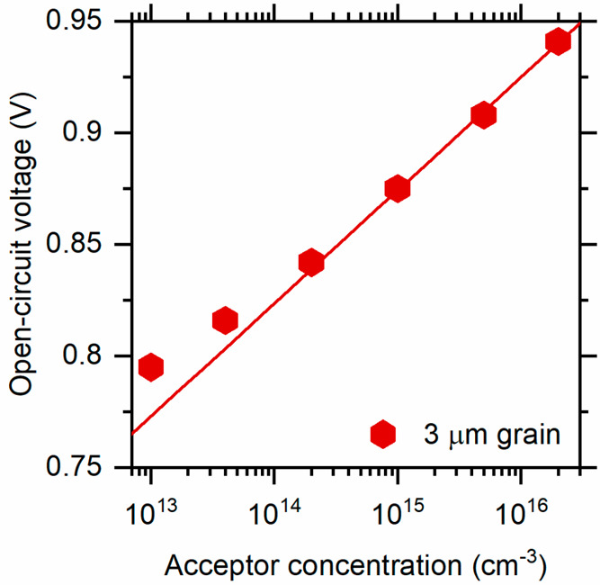
Dependence of the open-circuit voltage VOC (solar illumination) on the CdTe acceptor concentration NA. Symbols are numerical results obtained with an electron carrier mobility μe = 100 cm2/(V s) and 3 μm grain widths; the solid line is a least-squares fit to the three highest values and yields a slope of +50 mV/decade. The material model predicts a slope of +58 mV/decade at 300 K.
The two-dimensional simulations of Kanevce et al.(20) assumed negligible intragrain depletion, as we have here. Their simulations used μe = 320 cm2/V throughout but varied the grain boundary recombination velocity widely. Where there is overlap, their simulations agree well with the present simulations. This work also studied the effects of interface recombination at the CdS/CdTe interface, which reflects experiments consistent with this process. In experiments, the recombination shortcut to hot spots that we have identified in the present work would be difficult to distinguish from true interface recombination. The shortcut recombination mechanism has a significant dependence on the grain size as suggested by the lower panel of Figure 1. True interface recombination at the CdS/CdTe interface adds an additional recombination mechanism that would be independent of grain size. In cells with the grain boundary shortcut, materials processing that eliminates or passivates grain boundaries near the front junction could improve photovoltages by as much as 0.05 V. A difficulty is that extended defects such as dislocations and grain boundaries are difficult to terminate. It is possible that techniques for processing the CdS/CdTe interface, which are known to affect apparent interface recombination, are already passivating the near-interface region of CdTe.37 Recent technologies have improved the efficiency of CdS/CdTe cells by alloying CdTe with selenium (Se) near its interface with CdS. A study by Fiducia et al.(38) concludes that Se accumulates near the grain boundaries and passivates intragrain defects.
V. Conclusion
We compared an elementary model for the photovoltages obtainable from a polycrystalline material with numerical simulations of CdS/CdTe solar cells. The grain boundaries run through the p-type CdTe layer and perpendicular to its surface. Photocarrier recombination occurs at the grain boundaries and is diffusion-limited. The simulations incorporate device interfaces that might confound the elementary model, which predicts that the photovoltage should decline as −(kT/e) ln(μmin/θ2). Our major findings are the following:
The elementary absorber material model predicts the photovoltage in simulated cells well for a large range of μmin and θ. However, photovoltages from cell simulations are lower than the material model by a deficit of about 0.05–0.10 V.
The deficit is due to a shortcut for minority carrier photocurrents. The shortcut leads through the CdS to reach a recombination hot spot near the intersections with the grain boundaries. Experiments that are typically interpreted in terms of interface recombination would also be sensitive to the shortcut recombination mechanism.
For simplicity, grains that are parallel thin slabs running perpendicular to the cell surface are typically used in numerical simulations. The analytical material model was also solved here for cylindrical grains. For large grain boundary recombination velocities, cylindrical grains yield open-circuit voltages that are (kT/e) ln(8/3) smaller than with slab grains.
These results indicate the importance of passivation of the near-interface grain boundaries even in materials with low densities of intragrain recombination centers. In addition, the results presented here suggest at least two directions for future research in CdTe and other polycrystalline mosaic solar cells. The recombination hot spot at the grain boundary/emitter interface is responsible for a significant loss in cell efficiency. Research directed explicitly at visualizing, understanding, and passivating the hot spots could be productive. There may also be engineering strategies for the emitter/absorber interface region that would reduce their effect. Second, minority carrier mobility engineering is an opportunity for improved efficiency in the thin-film polycrystalline cells. The mobilities need to be as small as possible to build up the intragrain photocarrier concentration under illumination in the presence of grain boundary recombination but large enough to keep intragrain recombination under control. Direct measurements of carrier mobilities, in particular for thin-film CdTe, would be a useful counterpart for time-resolved photoluminescence and other indirect measurements.
Appendix. Diffusion-Limited Recombination in Cylindrical Columns
In a doped polycrystalline semiconductor under illumination, photocarrier transport in most regions is due to ambipolar diffusion of the minority carriers. For a p-type semiconductor, the minority carriers are electrons, and their density n(x,y,z) at steady-state can be described:
| A1 |
where D is the ambipolar diffusion coefficient for the carriers and G is the photogeneration rate, which we assume to be uniform. A simple case is a slab crystallite of thickness θ; Wight et al. provided the solution:1
| A2 |
where S is the recombination
velocity at the grain boundaries (x = θ/2 and x = −θ/2) and the corresponding boundary condition
at x = θ/2 is  . This
is the geometry assumed by the Sesame
code that we have used for the numerical calculations in the present
paper. The average lifetime of the electron photocarriers is defined
by using the average electron photocarrier density:
| A3 |
This yields the solution noted earlier:
| A4 |
For a cylindrical grain of diameter θ, the fundamental equation with cylindrical coordinates and symmetry is
| A5 |
where ρ is the distance of a point from
the cylinder axis. With the boundary condition  at ρ = θ/2,
the solution for
the density is
| A6 |
This leads to
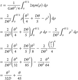 |
A7 |
For large recombination velocities, the assumption of slab grains geometry average yields lifetimes longer by 8/3 than assuming cylindrical grains. With small recombination velocities, the increase is 2-fold. The average lifetimes are converted to open-circuit voltages by using eq 1.
This research was partially supported by the National Science Foundation though Grants CBET-1336147 and CBET-1336134. The information, data, or work presented herein was funded in part by an award from the New York State Department of Economic Development (DED) to the Center of Excellence in Environmental & Energy Systems (SyracuseCoE) at Syracuse University. Any opinions, findings, conclusions, or recommendations expressed are those of the author(s) and do not necessarily reflect the views of the DED.
The authors declare no competing financial interest.
References
- Wight D. R.; Blenkinsop I. D.; Harding W.; Hamilton B. Diffusion-Limited Lifetime in Semiconductors. Phys. Rev. B: Condens. Matter Mater. Phys. 1981, 23, 5495–5510. 10.1103/PhysRevB.23.5495. [DOI] [Google Scholar]
- Donolato C. Modeling the Effect of Dislocations on the Minority Carrier Diffusion Length of a Semiconductor. J. Appl. Phys. 1998, 84, 2656–2664. 10.1063/1.368378. [DOI] [Google Scholar]
- Abbott M. D.; Bardos R. A.; Trupke T.; Fisher K. C.; Pink E. The Effect of Diffusion-Limited Lifetime on Implied Current Voltage Curves Based on Photoluminescence Data. J. Appl. Phys. 2007, 102, 044502. 10.1063/1.2756529. [DOI] [Google Scholar]
- Alberi K.; Branz H. M.; Guthrey H.; Romero M. J.; Martin I. T.; Teplin C. W.; Stradins P.; Young D. L. Dislocation-Limited Open Circuit Voltage in Film Crystal Silicon Solar Cells. Appl. Phys. Lett. 2012, 101, 123510. 10.1063/1.4754142. [DOI] [Google Scholar]; Note that eq 5 in this reference has been adapted as eq 1 in the text (n → Na, Nda2Dp → τ–1).
- Steffens S.; Becker C.; Amkreutz D.; Klossek A.; Kittler M.; Chen Y.-Y.; Schnegg A.; Klingsporn M.; Abou-Ras D.; Lips K.; Rech B. Impact of Dislocations and Dangling Bond Defects on the Electrical Performance of Crystalline Silicon Thin Films. Appl. Phys. Lett. 2014, 105, 022108. 10.1063/1.4890625. [DOI] [Google Scholar]
- Woo S.; Bertoni M.; Choi K.; Nam S.; Castellanos S.; Powell D. M.; Buonassisi T.; Choi H. An Insight into Dislocation Density Reduction in Multicrystalline Silicon. Sol. Energy Mater. Sol. Cells 2016, 155, 88–100. 10.1016/j.solmat.2016.03.040. [DOI] [Google Scholar]
- Ščajev P.; Usikov A.; Soukhoveev V.; Aleksieju̅nas R.; Jarašiu̅nas K. Anisotropy of Free-Carrier Absorption and Diffusivity in m-plane GaN. Appl. Phys. Lett. 2011, 98, 202105. 10.1063/1.3591173. [DOI] [Google Scholar]
- Jiang C.; Zhang P. Crystalline Orientation Dependent Photoresponse and Heterogeneous Behaviors of Grain Boundaries in Perovskite Solar Cells. J. Appl. Phys. 2018, 123, 083105. 10.1063/1.5007857. [DOI] [Google Scholar]
- Nelson J. Diffusion-limited Recombination in Polymer-fullerene Blends and its Influence on Photocurrent Collection. Phys. Rev. B: Condens. Matter Mater. Phys. 2003, 67, 155209. 10.1103/PhysRevB.67.155209. [DOI] [Google Scholar]
- Kopidakis N.; Benkstein K. D.; van de Lagemaat J.; Frank A. J. Transport-Limited Recombination of Photocarriers in Dye-Sensitized Nanocrystalline TiO2 Solar Cells. J. Phys. Chem. B 2003, 107, 11307–11315. 10.1021/jp0304475. [DOI] [Google Scholar]
- Assuming that the minority carrier density is much smaller than the majority carrier density, the ambipolar diffusion constant Damb is essentially equal to the minority carrier diffusion constant Dmin. The Einstein relation yields Dmin = (kBT/e)μmin, where μmin is the minority carrier mobility and kBT/e is the ratio of the thermal energy to the electronic charge. See: Würfel P.Physics of Solar Cells: From Principles to New Concept; Wiley-VCH Verlag GmbH & Co. KGaA: Weinheim, 2005; pp 101–103. [Google Scholar]
- Bhattacharya S.; John S. Beyond 30% Conversion Efficiency in Silicon Solar Cells: A Numerical Demonstration. Sci. Rep. 2019, 9, 12482. 10.1038/s41598-019-48981-w. [DOI] [PMC free article] [PubMed] [Google Scholar]
- Green M. A.; Dunlop E. D.; Hohl-Ebinger J.; Yoshita M.; Kopidakis N.; Hao X. Solar Cell Efficiency Tables (Version 56). Prog. Photovoltaics 2020, 28, 629–638. 10.1002/pip.3303. [DOI] [Google Scholar]
- Burst J. M.; Duenow J. N.; Albin D. S.; Colegrove E.; Reese M. O.; Aguiar J. A.; Jiang C.-S.; Patel M. K.; Al-Jassim M. M.; Kuciauskas D.; Swain S.; Ablekim T.; Lynn K. G.; Metzger W. K. CdTe Solar Cells with Open-Circuit Voltage Breaking the 1V Barrier. Nat. Energy 2016, 1, 16015. 10.1038/nenergy.2016.15. [DOI] [Google Scholar]
- Zhao Y.; Boccard M.; Liu S.; Becker J.; Zhao X.-H.; Campbell C. M.; Suarez E.; Lassise M. B.; Holman Z.; Zhang Y.-H. Monocrystalline CdTe Solar Cells with Open-Circuit Voltage Over 1 V and Efficiency of 17%. Nat. Energy 2016, 1, 16067. 10.1038/nenergy.2016.67. [DOI] [Google Scholar]
- Gaury B.; Sun Y.; Bermel P.; Haney P. M. Sesame: A 2-Dimensional Solar Cell Modeling Tool. Sol. Energy Mater. Sol. Cells 2019, 198, 53–62. 10.1016/j.solmat.2019.03.037. [DOI] [PMC free article] [PubMed] [Google Scholar]
- Gaury B.; Haney P. Charged Grain Boundaries and Carrier Recombination in Polycrystalline Thin-Film Solar Cells. Phys. Rev. Appl. 2017, 8, 054026. 10.1103/PhysRevApplied.8.054026. [DOI] [Google Scholar]
- Gaury B.; Haney P. M. Quantitative Theory of the Grain Boundary Impact on the Open-Circuit Voltage of Polycrystalline Solar Cells. ACS Appl. Energy Mater. 2019, 2, 144–151. 10.1021/acsaem.8b01246. [DOI] [Google Scholar]
- Hegedus S.; Desai D.; Thompson C. Voltage Dependent Photocurrent Collection in CdTe/CdS Solar Cells. Prog. Photovoltaics 2007, 15, 587–602. 10.1002/pip.767. [DOI] [Google Scholar]
- Kanevce A.; Reese M. O.; Barnes T. M.; Jensen S. A.; Metzger W. K. The Roles of Carrier Concentration and Interface, Bulk, and Grain-Boundary Recombination for 25% Efficient CdTe Solar Cells. J. Appl. Phys. 2017, 121, 214506. 10.1063/1.4984320. [DOI] [Google Scholar]
- Troni F.; Menozzi R.; Colegrove E.; Buurma C. Simulation of Current Transport in Polycrystalline CdTe Solar Cells. J. Electron. Mater. 2013, 42, 3175–3180. 10.1007/s11664-013-2702-0. [DOI] [Google Scholar]
- Mungan E. S.; Dongaonkar S.; Alam M. A.. Bridging the Gap: Modeling the Variation due to Grain Size Distribution in CdTe Solar Cells. In 2013 IEEE 39th Photovoltaic Specialists Conference (PVSC), Tampa, FL, 16–21 June 2013; pp 2007–2010.
- Jin Y.; Dunham S. T. The Impact of Charged Grain Boundaries on CdTe Solar Cell: EBIC Measurements Not Predictive of Device Performance. IEEE J. Photovolt. 2017, 7, 329–334. 10.1109/JPHOTOV.2016.2631298. [DOI] [Google Scholar]
- Gaury B.; Haney P. Charged Grain Boundaries Reduce the Open-Circuit Voltage of Polycrystalline Solar Cells—An Analytical Description. J. Appl. Phys. 2016, 120, 234503. 10.1063/1.4972028. [DOI] [PMC free article] [PubMed] [Google Scholar]
- Green M. A. Bounds upon Grain Boundary Effects in Minority Carrier Semiconductor Devices: A Rigorous ‘Perturbation’ Approach with Application to Silicon Solar Cells. J. Appl. Phys. 1996, 80, 1515–1521. 10.1063/1.363022. [DOI] [Google Scholar]
- Schiff E. A. Low-Mobility Solar Cells: A Device-Physics Primer with Application to Amorphous Silicon. Sol. Energy Mater. Sol. Cells 2003, 78, 567–595. 10.1016/S0927-0248(02)00452-X. [DOI] [Google Scholar]
- Reference global Air Mass 1.5 (ASTM G-173-03) standard spectrum for terrestrial solar cell measurements was taken from NREL’s website: https://www.nrel.gov/grid/solar-resource/spectra-am1.5.html (accessed: January 2020).
- Adachi S.Wurtzite Cadmium Sulphide (w-CdS). In Optical Constants of Crystalline and Amorphous Semiconductors; Springer: Boston, MA, 1999; pp 517–529. [Google Scholar]
- Adachi S.Cadmium Telluride (CdTe). In Optical Constants of Crystalline and Amorphous Semiconductors; Springer: Boston, MA, 1999; pp 538–545. [Google Scholar]
- Metzger W. K.; Grover S.; Lu D.; Colegrove E.; Moseley J.; Perkins C. L.; Li X.; Mallick R.; Zhang W.; Malik R.; Kephart J.; Jiang C.-S.; Kuciauskas D.; Albin D. S.; Al-Jassim M. M.; Xiong G.; Gloeckler M. Exceeding 20% Efficiency Within Situ Group V doping in Polycrystalline CdTe Solar Cells. Nat. Energy 2019, 4, 837–845. 10.1038/s41560-019-0446-7. [DOI] [Google Scholar]
- Duenow J. N.; Metzger W. K. Back-Surface Recombination, Electron Reflectors, and Paths to 28% Efficiency for Thin-Film Photovoltaics: A CdTe Case Study. J. Appl. Phys. 2019, 125, 053101. 10.1063/1.5063799. [DOI] [Google Scholar]
- Material parameters for CdTe layer: conduction band effective density of states Nc = 7.94 × 1017 cm–3 and valence band effective density of states Nv = 1.80 × 1019 cm–3. Material parameters for CdS layer: Nc = 2.24 × 1018 cm–3 and Nv = 1.80 × 1019 cm–3.
- Moseley J.; Rale P.; Collin S.; Colegrove E.; Guthrey H.; Kuciauskas D.; Moutinho H.; Al-Jassim M. M.; Metzger W. K. Luminescence Methodology to Determine Grain-Boundary, Grain-Interior, and Surface Recombination in Thin-Film Solar Cells. J. Appl. Phys. 2018, 124, 113104. 10.1063/1.5042532. [DOI] [Google Scholar]
- For p-type CdTe material, for each electron carrier mobility, μe, the lifetime for the electrons, τe, was adjusted to keep the ambipolar diffusion length, LD, greater than the width of the grains, θ, in the dark. The Sesame code assumes deep-level recombination centers and uses the Shockley–Read–Hall (SRH) formula to calculate recombination rates. The formula uses electron lifetime and hole lifetime parameters τe and τh. For electrons in a p-type material, the SRH lifetime parameter is essentially equal to the actual electron lifetime. The SRH formula also uses the defect level energy Et relative to a midgap reference location. We set τh = τe and Et = 0; these parameters have little, if any, effect on the present calculations.
- Fonash S. J.Solar Cell Device Physics, 2nd ed.; Academic Press: Burlington, MA, 2010. [Google Scholar]
- Jiang C.-S.; Moutinho H. R.; Moseley J.; Kanevce A.; Duenow J. N.; Colegrove E.; Xiao C.; Metzger W. K.; Al-Jassim M. M.. Simultaneous Examination of Grain-Boundary Potential, Recombination, and Photocurrent in CdTe Solar Cells Using Diverse Nanometer-Scale Imaging. In 2017 IEEE 44th Photovoltaic Specialist Conference (PVSC), Washington, DC, 25–30 June 2017; pp 1312–1316.
- Metzger W. K.; Albin D.; Romero M. J.; Dippo P.; Young M. CdCl2 Treatment, S Diffusion, and Recombination in Polycrystalline CdTe. J. Appl. Phys. 2006, 99, 103703. 10.1063/1.2196127. [DOI] [Google Scholar]
- Fiducia T. A. M.; Mendis B. G.; Li K.; Grovenor C. R. M.; Munshi A. H.; Barth K.; Sampath W. S.; Wright L. D.; Abbas A.; Bowers J. W.; Walls J. M. Understanding the Role of Selenium in Defect Passivation for Highly Efficient Selenium-alloyed Cadmium Telluride Solar Cells. Nat. Energy 2019, 4, 504–511. 10.1038/s41560-019-0389-z. [DOI] [Google Scholar]


