

Abstract

Two-dimensional (2D) perovskites are emerging as promising candidates for diverse optoelectronic applications because of low cost and excellent stability. In this work, we explore the electronic structures and interfacial properties of (4Tm)2PbI4 with both the collinear and noncollinear DFT (PBE and HSE06) methods. The results evidently manifest that explicitly considering the spin–orbit coupling (SOC) effects is necessary to attain correct band alignment of (4Tm)2PbI4 that agrees with recent experiments (Nat. Chem. 2019, 11, 115131712613; Nature 2020, 580, 61432350477). The subsequent time-domain noncollinear DFT-based nonadiabatic carrier dynamics simulations with the SOC effects reveal that the photoinduced electron and hole transfer processes are asymmetric and associated with different rates. The differences are mainly ascribed to considerably different nonadiabatic couplings in charge of the electron and hole transfer processes. Shortly, our current work sheds important light on the mechanism of the interfacial charge carrier transfer processes of (4Tm)2PbI4. The importance of the SOC effects on correctly aligning the band states of (4Tm)2PbI4 may be generalized to similar organic–inorganic hybrid 2D perovskites having heavy Pb atoms.
Keywords: spin−orbit couplings, interfacial properties, perovskite heterojunctions, photoinduced carrier dynamics, two-component noncollinear DFT calculations
1. Introduction
Organic–inorganic lead halide perovskites have revolutionized many research fields, e.g., optoelectronics and photovoltaics,1−3 since the seminal work of Kojima and co-workers in 2009.4 As a paradigm, three-dimensional (3D) perovskites have been extensively explored in the past decade as promising optoelectronic materials in solar cells, light-emitting diodes, and photodetectors.3,5−9 However, these bulk perovskites are intrinsically vulnerable to moisture, oxygen, light, heat, etc., which makes them unstable and easy to degrade under ambient conditions.10−17 These shortcomings severely hinder their further developments and potential applications. To alleviate these critical problems, many different strategies are proposed, one of which is using two-dimensional (2D) perovskites as photoactive materials in optoelectronic devices, which greatly improves their long-term stability and water resistance.18−22
2D Ruddlesden–Popper (RP) phase perovskites have a general formula (RNH3)2An–1MnX3n+1 (n = 1, 2, 3, 4....), in which RNH3 is a large monovalent aliphatic or aromatic alkylammonium organic cation (e.g., butylammonium, etc.); A is a small monovalent organic cation (e.g., methylammonium, etc.); M is a divalent metal cation (e.g., Pb2+, etc.); X is a halide anion (e.g., Cl–, etc.); and n represents the number of M-centered octahedral layers. Structurally, 2D perovskites can be understood as thin slabs that are cut from 3D counterparts along certain crystal indices. These thin perovskite slabs can further be sandwiched by two-layer organic ligands, which finally forms quantum wells by periodically repeating organic and inorganic layers along the out-of-plane growth direction to provide flexible tunability for their structures and properties.23−36
The earliest research on 2D perovskites was in the 1990s;37−41 and recent years have witnessed a rapidly increasing number of experimental studies on exploring the optoelectronic properties of 2D perovskites. For example, Zhang et al. reported 2D perovskite photovoltaic devices of (AA)2(MA)3Pb4I13 (AA = amylamine, MA = methylammonium) with a high power conversion efficiency (18.42%).42 Huang et al. demonstrated that solution-processed 2D perovskite light-emitting diodes have excellent film morphologies and exhibit high external quantum efficiency (11.7%).43 Nonetheless, many challenges that need to be overcome prior to 2D perovskite materials having potential applications in practical optoelectronic devices still remain.
In most 2D perovskites, insulating aliphatic ammonium cations are chosen as organic layers, which give rise to poor charge transporting performances. So how to design and synthesize new organic layers which can participate in charge transfer to expand the wide application of 2D perovskites in optoelectronic materials is an urgent task to be solved. Very recently, in order to expand the range of organic cations that are used as organic layers separating inorganic [MX6]4– octahedral layers in 2D perovskites, Dou et al. employed organic chemistry principles to develop a robust molecular design strategy and successfully synthesized several highly quality hybrid quantum wells with tailored optoelectronic properties, for example, (4Tm)2PbI4, (4TCNm)2PbI4, (2T)2PbI4, and (BTm)2PbI4.44 Among them, (4Tm)2PbI4 and (4TCNm)2PbI4 possess a Type-II band alignment, where 4Tm and 4TCNm have good charge transfer abilities. This was confirmed by time- and spectral-resolved photoluminescence spectroscopy analysis, and the photoinduced interfacial charge transfer processes are suggested to quench the photoluminescence. The charge transfer time at the organic–inorganic interfaces of (4Tm)2PbI4 and (4TCNm)2PbI4 is estimated to be 3.8 and 4.3 ps, respectively. And the generated charge-separated state is found to be long-lived for several nanoseconds.45 These experimental results provide preliminary and valuable information on interfacial carrier dynamics of (4Tm)2PbI4 and (4TCNm)2PbI4. However, many ambiguous mechanistic details remain to be resolved. Unfortunately, until now, there is no theoretical work reported to explore their electronic structures and interfacial properties.
Computationally, there are a few theoretical works focused on exploring static and dynamical interfacial and optoelectronic properties. Wei et al. performed DFT calculations to explore the thermodynamic stability of 2D perovskites and found that their stability originates from the asymmetric surface properties.18 Lu et al. employed molecular design strategies to construct several 2D perovskites with desirable intramolecular band alignments, which could have potential for light-emitting diode and photovoltaic applications.46 In addition to static properties, dynamical properties were also extensively explored by the Prezhdo, Tretiak, Neukirch, Brédas, and Zhao groups who have studied photoinduced carrier dynamics and lifetimes, nonradiative electron–hole recombination of a series of 2D perovskites (Dion-Jacobson and Ruddlesden–Popper phases) with varying organic spacers, and perovskite compositions by means of time-domain nonadiabatic molecular dynamics simulations. However, there is no theoretical work reported that explores electronic structures and interfacial properties of the above-mentioned (4Tm)2PbI4.23,28,47−49
On the other hand, (4Tm)2PbI4 contains heavy Pb and I atoms, which are widely known to have non-negligible spin–orbit couplings (SOCs). However, it has long been ignored in previous nonadiabatic dynamic simulations.23,28,49 Recent two-component DFT-based nonadiabatic dynamics simulations by Akimov et al. and Mohammed et al. revealed that the SOC effect can greatly speed up electron and hole cooling dynamics of bulk and 2D perovskite materials.50,51 Recently, we have also employed our developed time-domain noncollinear DFT-based nonadiabatic dynamics approach to simulate charge transfer dynamics at the interface of a fullerene-passivated perovskite model and found that the SOC effects can heavily accelerate such an electron transfer process.52
Motivated by the above questions, in this work, we have first employed both the collinear and noncollinear DFT (PBE and HSE06) methods to explore the electronic structures and interfacial properties of (4Tm)2PbI4.53−57 The results show that the SOC effects are indispensable for correctly aligning band states between individual components of (4Tm)2PbI4. Subsequently, we use the developed two-component noncollinear DFT-based nonadiabatic dynamics approach to simulate light-driven electron and hole transfer processes, which reveal that these two processes are asymmetric and associated with different rates. Further analysis shows that these differences stem from quite different nonadiabatic couplings.
2. Computational Methods
We first construct a 2 × 1 (4Tm)2PbI4 (100) surface model based on the previously reported crystal structure, which is in accordance with the single quantum-well structure obtained by experiment.44 In order to prevent the interactions between two neighboring images, we add a vacuum layer of 25 Å along the direction perpendicular to the slab. The resulting cell parameters of (4Tm)2PbI4 used for calculation are 12.19, 12.21, and 52.02 Å. Geometry optimization calculations are carried out with the Vienna Ab initio Simulation Package (VASP) with projector-augmented-wave (PAW) pseudopotentials.58−62 The Perdew–Burke–Ernzerhof (PBE) functional is used to describe electronic exchange-correlation interaction in geometry optimizations.55,56 And the DFT-D3 method with Becke–Johnson damping proposed by Grimme et al. is used to describe the van der Waals interaction in the 2D perovskite.63 Based on the optimized structure of PBE+D3, we calculate the PDOS using the PBE+D3, PBE+D3+SOC, HSE06+D3, and HSE06+D3+SOC methods.57 The SOC effects are explicitly considered by using the noncollinear DFT method implemented in VASP.53,54
The ab initio molecular dynamics simulations are carried out using the DFT method implemented in the Quickstep module of the CP2K package.64,65 The PBE+D3 method and mixed Gaussian and plane wave basis sets with an energy cutoff of 400 Ry are used. Accordingly, the DZVP-MOLOPT-SR-GTH basis sets and Goedecker–Teter–Hutter pseudopotentials are employed throughout all CP2K calculations.66−70 Due to the large size of the simulated system, only the gamma point is used in all DFT calculations. In canonical molecular dynamics simulations, the system is first heated to 300 K and equilibrated for 1 ps in which a time step of 1 fs is used for nuclear propagation and a velocity rescaling thermostat technique is used to control the temperature.71 After that, a 1 ps microcanonical molecular dynamics simulation is conducted with the same 1 fs time step. Finally, this 1 ps trajectory is iterated four times to obtain a 4 ps trajectory, which is used to study charge carrier transfer dynamics. This iterative strategy has been widely used in similar researches by Prezhdo and co-workers.72−74 From the generated MD trajectories, 500 different initial conditions are generated and for each initial condition, 500 surface hopping trajectories are run. Therefore, a total of 500 × 500 trajectories are run in subsequent noncollinear DFT-based nonadiabatic dynamics simulations and the final results are averaged over all these trajectories. Energies of all relevant adiabatic states and interstate couplings that are needed for nonadiabatic dynamics simulations are calculated using the noncollinear PBE+SOC+D3 method implemented in a locally modified OPENMX3.9 package.75−77 The empirical quantum decoherence correction (0.1 au) of Granucci et al. is used in the surface-hopping dynamics simulations.78
3. Results and Discussion
The crystal structure of (4Tm)2PbI4 is characterized by the recent experimental work44 in which Dou et al. confirmed that its thickness satisfies a single quantum-well structure with only one-layer PbI4 unit that is sandwiched between two layers of the 4Tm ligands. Based on this crystal structure, we construct a computational model as shown in Figure 1, which has 380 atoms in a repeating unit. In the PBE+D3 optimized structure, the Pb ions deviate slightly from the central position of the PbI4 octahedrons toward one of the apical I atoms but away from the other I atoms, which gives rise to three types of Pb–I bonds. In the first two, the Pb atom is separately bonded with one of the two apical I atoms with the calculated bond lengths of about 3.1 and 3.5 Å. In the last one, the Pb atom is bonded with one of the four equatorial I atoms and their bond lengths are calculated to be around 3.2 Å, respectively (see Figure S1 for specific values). Note that these theoretically estimated bond lengths are in good agreement with experimental values.44 The 4Tm ligand is, from the two sides, coordinated with the central PbI4 unit through the terminal positively charged RNH3 group. In addition, there exists a clear intermolecular π–π interaction between the tetrathiophene moieties of the nearby 4Tm ligands. The interdistance between 4Tm ligands is on average about 3 Å at the PBE+D3 level. The parallel arrangement of the 4Tm ligands is used to not only passivate surface trap states of the exposed PbI4 units but also improve the perovskite stability.
Figure 1.

Structure of (4Tm)2PbI4 optimized by the PBE+D3 method. Inside the blue box is a periodically repeating unit. Purple, I atoms; white, H atoms; blue, N atoms; brown, C atoms; yellow, S atoms; gray, Pb atoms. Octahedrons represent the PbI4 units.
The projected density of states (PDOS) is very useful for understanding electronic structures, band gaps, energy alignments of materials, and their individual components. Early studies on electronic structures of perovskite materials were always carried out with conventional collinear DFT calculations in which scalar relativistic effects are implicitly included via pseudopotentials. However, many recent theoretical works have shown that explicitly including the spin–orbit interaction in the DFT self-consistent field calculations are indispensable for achieving reasonably accurate energy alignments.46,50−52 Such calculations call for two-component noncollinear DFT calculations in which spinor orbitals are used as molecular bases and an explicit spin–orbit operator is added in the electronic Hamiltonian.53,54 In order to quantify the impact of the SOC effects on the PDOS of (4Tm)2PbI4, we first calculate the PDOS results at the PBE+D3, HSE06+D3, PBE+D3+SOC, and HSE06+D3+SOC levels in the framework of the collinear and noncollinear DFT methods. The computational results are shown in Figure 2 and Table 1, from which two interesting points can be drawn for band gaps of the total (4Tm)2PbI4 system. First, regardless of whether the SOC effects are considered, the HSE06 functional gives much larger band gaps than the PBE functional for the whole system, for example, 1.69 vs 2.33 eV [1.22 vs 1.79 eV] without [with] the SOC effects in Table 1. Second, the SOC effects reduce band gaps at either the PBE or HSE06 levels, e.g., 1.69 [2.33] eV at PBE+D3 [HSE06+D3] vs 1.22 [1.79] eV at PBE+D3+SOC [HSE06+D3+SOC]. Due to these effects, one can get close band gaps between the PBE+D3 and HSE06+D3+SOC methods, 1.69 vs 1.79 eV. But, one should be noted that the close value obtained by PBE is just a coincidence due to neglecting the SOC effects and underestimation of the band gap calculated by PBE. In order to show the SOC effects in a quantitative way, we have used the noncollinear PBE+D3 calculations with and without the SOC effects to calculate the averaged energy differences of the Kohn–Sham orbitals of 4Tm and PbI4, which are estimated to be 0.01 and 0.35 eV, respectively. These data reveal the indispensable role of the SOC effects in the correct description of PbI4 and Pb-containing perovskites.
Figure 2.

PDOS of (4Tm)2PbI4 calculated with (a) PBE+D3, (b) PBE+D3+SOC, (c) HSE06+D3, and (d) HSE06+D3+SOC methods. Green, 4Tm; blue, PbI4. Fermi level is chosen as the zero point.
Table 1. Band Gaps (in eV) of (4Tm)2PbI4 and Its 4Tm and PbI4 Components Calculated by Different Collinear and Noncollinear DFT Methods without and with the SOC Effects.
| components | PBE+D3 | HSE06+D3 | PBE+D3+SOC | HSE06+D3+SOC |
|---|---|---|---|---|
| 4Tm | 1.69 | 2.33 | 1.70 | 2.34 |
| PbI4 | 2.36 | 3.08 | 1.62 | 2.30 |
| (4Tm)2PbI4 | 1.69 | 2.33 | 1.22 | 1.79 |
More importantly, as shown in Figure 2a and c, (4Tm)2PbI4 has a Type-I band alignment between 4Tm and PbI4 at either the PBE or HSE06 level. However, once the SOC effects are included, a correct Type-II band alignment which was confirmed by Dou et al. is reproduced,44,45,79 as shown in Figure 2b and d. This interesting phenomenon occurs because the influences of the SOC effects on PbI4 and 4Tm are not the same. For the former, the SOC effects narrow the band gap by 0.74 and 0.78 eV at the PBE and HSE06 levels, respectively, while, for the latter, it is negligible within 0.01 eV (see Table 1). This implies the SOC effects must be considered for the correct description of the interfacial energy levels of (4Tm)2PbI4. This phenomenon is also expected to take place in other organic–inorganic hybrid systems having heavy atoms with remarkable SOC effects.46
To further verify the switch of the band alignment of (4Tm)2PbI4 from Type-I to -II upon including the SOC effects, the corresponding band structures are also calculated at the PBE and PBE+SOC levels, as shown in Figure 3. It is clear that (4Tm)2PbI4 is a direct band gap semiconductor with both a valence band maximum (VBM) and conduction band minimum (CBM) at the G point. Clearly, SOC mainly has significant effects on the bands of PbI4 which contains heavy atoms, and it does not change the bands of 4Tm which consisted of C, N, H, and S. At the PBE level, both the CBM and VBM states of (4Tm)2PbI4 are very flat along the K-point path, and importantly, they all originate from 4Tm (see Figure 3a). In other words, (4Tm)2PbI4 has a Type-I band alignment. However, considering the SOC effects leads to a Type-II band alignment. This can be attributed to the fact that the SOC effects cause the splitting of the conduction band of PbI4, making it become the CBM state of (4Tm)2PbI4 at the G point. This phenomenon exists along the studied K-point path except that near the M point. Therefore, it is clear that the SOC effects change the relative energy levels of the conduction bands of both 4Tm and PbI4 components of (4Tm)2PbI4, which will undoubtedly affect the photoinduced electron relaxation process, just as in 3D perovskites.51
Figure 3.

Band structures of (4Tm)2PbI4 calculated with (a) PBE+D3 and (b) PBE+D3+SOC methods (red lines, 4Tm; blue lines, PbI4). Fermi level is chosen as the zero point.
Specifically, (4Tm)2PbI4 is a Type-II heterojunction according to the band alignment of 4Tm and PbI4, as shown in Figure 2b and d. Electronic structure calculations show that 4Tm and PbI4 have similar band gaps of ca. 2.30 eV, and in the present study only the minimum photoexcitation promoting an electron from the VBM to CBM states is considered. As a consequence, the 4Tm photoexcitation will favor an interfacial electron transfer to PbI4, whereas that of PbI4 does an interfacial hole transfer to 4Tm. Nonetheless, many mechanistic details related to these interfacial charge carrier dynamics are ambiguous. To resolve these issues, we carry out time-domain noncollinear DFT-based nonadiabatic dynamics simulations to explore related interfacial charge carrier transfer processes. From Figure 2 and Table 1, it is clear that both the PBE+D3+SOC and HSE06+D3+SOC functionals give a highly similar energy-level alignment of PbI4 and 4Tm. Considering the computational efficiency, the PBE+D3+SOC method is employed to simulate the interfacial charge carrier dynamics. In this work, we are merely focused on the interfacial electron and hole transfer dynamics starting from the CBM state of 4Tm and the VBM state of PbI4, respectively.
Figure 4 collects the band-edge states of 4Tm and PbI4 in (4Tm)2PbI4. Both the CBM and VBM states of 4Tm stem from the contribution of p orbitals of the tetrathiophene moiety of 4Tm. The CBM state of PbI4 is mainly distributed within the horizontal of the octahedral layer (negligible contribution from the two apical I atoms) and is mainly composed of 6p orbitals of Pb atoms as well as small contribution of 5p orbitals of I atoms. Differently, the VBM state of PbI4 is mainly attributed to 5p orbitals of I atoms and 6s orbitals of Pb atoms. Interestingly, this state is distributed in the entire octahedral layer, and more importantly its apical I atoms have a comparable contribution. As a result of this feature, the VBM states of PbI4 and 4Tm have a much better spatial overlap than those related to the CBM states, which will benefit the interfacial hole transfer (see below).
Figure 4.

PBE+D3+SOC calculated charge densities of the CBM and VBM states of both 4Tm and PbI4 that are involved in the interfacial hole and electron transfer dynamics.
Next, let us focus on the interfacial electron and hole transfer dynamics. As shown in Figure 5a, the interfacial electron transfer dynamics exhibits two different stages. In the first stage, an ultrafast electron transfer process takes place, during which about 12% of the electron population is transferred from 4Tm to PbI4 within 200 fs. But, in the following 800 fs, the electron transfer is very slow. Through fitting the time-dependent electron population with a double-exponential decay function, one can obtain two fitted time constants of 53 fs and 64.5 ps. In stark contrast, the interfacial hole transfer is much simpler and only one monotonic decrease of the hole population to about 10% is involved in the 1 ps nonadiabatic dynamics simulation. Similarly, a time constant of 1.4 ps is obtained via fitting the corresponding time-dependent hole population with a single-exponential decay function.
Figure 5.

Time-dependent (a) electron and (b) hole populations separately localized on 4Tm and PbI4 of (4Tm)2PbI4; distribution of energy gaps (in kcal/mol) (c) between the CBM states of PbI4 and 4Tm and (d) between the VBM_PbI4 and VBM-7_4Tm states.
How to understand the differences of the above dynamical processes? First, we focus on the electron transfer process. As shown in Figure S2, PbI4 provides one acceptor conduction band state to accept the electron from the CBM state of 4Tm; in addition, the CBM state of 4Tm has some clear spatial overlap with the CBM+1 state of PbI4, so that one can see an ultrafast interfacial electron transfer in the very beginning (fitted time constant: 53 fs, in Figure 5a). But, due to the fact that the CBM state of 4Tm is lower in energy than the CBM+1 state of PbI4 along the trajectory, only 12% of the electron amount is transferred from 4Tm to PbI4 in the first stage. In comparison, the remaining 88% of the electron amount will stay in the CBM state of 4Tm for a while because of an obvious energy gap between the CBM states of PbI4 and 4Tm. As depicted in Figure 5c, this energy gap ranges from 2 to 12 kcal/mol along the trajectory with an averaged value of 6.4 kcal/mol. In contrast, for the hole transfer process, there are eight acceptor states within 4Tm to accept the hole from the VBM state of PbI4. Among them, VBM-7_4Tm is the closest to VBM_PbI4 in energy. As shown in Figure 5d, the energy gap between VBM_PbI4 and VBM-7_4Tm is also small, which is on average 5.4 kcal/mol, ranging from 1 to 10 kcal/mol. This comparably smaller energy gap makes the hole transfer a little favorable than the electron transfer. Yet, to be honest, such a small difference between these two averaged energy gaps (with ca. 1 kcal/mol) should be not the foremost factor in charge of the distinct dynamical behaviors of the interfacial hole and electron transfer processes.
It
is well-known that, in addition to energy gaps, nonadiabatic
couplings are another important factor that determines whether nonadiabatic
transition occurs efficiently. The nonadiabatic coupling djk between two relevant states is expressed
as 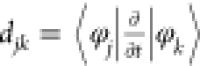 in which φj and φk are wave functions
of states j and k. This equation
can be also converted via the chain rule of calculus into
in which φj and φk are wave functions
of states j and k. This equation
can be also converted via the chain rule of calculus into
from which it is clear that the nonadiabatic coupling is heavily related to two quantities, the energy difference (denominator) and interstate coupling (numerator) of the two states. Which one is the main determinant to enhance the nonadiabatic coupling is obviously system-dependent. In most cases of dynamics simulations of materials, the energy difference is dominant while the wave function properties keep essentially constant. However, the interstate coupling based on the wave function properties can also become major in the present work. As discussed above, the averaged energy differences in both the electron and hole transfer processes are close to each other within 1 kcal/mol. Such subtle difference should not be responsible for so remarkably distinct charge transfer times (64.5 versus 1.4 ps). Instead, the distinct wave function properties relevant to the electron and hole transfer processes are major. As discussed above, the VBM states of PbI4 and 4Tm are spatially closer to each other than their CBMs (Figure S3). This is also supported by the calculated nonadiabatic couplings. As shown in Table 2, the nonadiabatic coupling between the VBM_PbI4 and VBM-7_4Tm states is more than 3 times larger than that between the CBM_ PbI4 and CBM_4TM states (2.76 and 0.78 meV). Therefore, the significantly different nonadiabatic couplings are in charge of the distinct electron and hole transfer dynamical behaviors observed in the present simulations.
Table 2. PBE+D3+SOC Calculated Nonadiabatic Coupling (meV) of Relevant CBM and Valence Band States of 4Tm and PbI4 in (4Tm)2PbI4.
| coupling | CBM_PbI4/CBM_4Tm | VBM_PbI4/VBM-7_4Tm |
|---|---|---|
| 4Tm and PbI4 | 0.78 | 2.76 |
Figure 6 summarizes the mechanism for the interfacial carrier transfer processes of (4Tm)2PbI4 upon the band-edge photoexcitation. When 4Tm is excited, an electron that is originally in the VBM_4Tm state is promoted into the CBM_4Tm state, which meanwhile produces a hole in VBM_4Tm. In such a case, only the interfacial electron transfer process from 4Tm to PbI4 is thermodynamically allowed because the CBM_4Tm state is much higher than the CBM_PbI4 state. Owing to the significant overlap between the CBM_4Tm and CBM+1_PbI4 states, an ultrafast electron transfer is observed, which is mainly ascribed to the adiabatic atomic motion. However, the subsequent electron cooling process from the CBM+1 to CBM states of PbI4 is heavily inhibited because of the large energy gap between such two states (see Figure S2). These viewpoints are also supported by the two time constants of 53 fs and 64.5 ps estimated through fitting of the time-dependent electron population in Figure 5a. Differently, the PbI4 photoexcitation only allows the interfacial hole transfer to 4Tm because the excited electron, in such a case, occupies the lowest CBM_PbI4 state, which is much lower than the CBM_4Tm state. The interfacial hole transfer process is favorable due to the smaller energy gap and comparably larger nonadiabatic coupling between the VBM state of 4Tm and VBM-7 state of PbI4 in comparison with the above interfacial electron transfer. The related time constant is estimated to be 1.4 ps according to the fitting of the time-dependent hole population via a simple single-exponential equation in Figure 5b.
Figure 6.

Schematic mechanism for the charge carrier transfer processes taking place at the interface of (4Tm)2PbI4.
The presently suggested mechanism rationalizes the recent experiments by Dou et al. in which the photoluminescence images and spectra of (4Tm)2PbI4 is measured to be negligibly weak.44 To interpret the experimental phenomena, they suggested a Type-II interface for (4Tm)2PbI4 so that the interfacial charge carrier transfer processes could quench the luminescence. This property is confirmed by our present DFT calculations and dynamics simulations. However, it should be stressed again that, due to the significant SOC effects on the Pb-containing inorganic layer of (4Tm)2PbI4, it is necessary to include these non-negligible effects in the correct theoretical description of its interfacial properties. Specifically, without including these effects, it is a Type-I interface, which is inconsistent with the experimental results.
In addition, Dou et al. have explored the interfacial charge transfer process of (4Tm)2PbI4 using the time-resolved photoluminescence spectroscopy with a time resolution of 2 ps.44 The significant quenching of the photoluminescence intensity is consistent with the suggested Type-II band alignment, which allows efficient charge transfer at the interface of the organic and inorganic layers. In terms of the fast component of the photoluminescence decay from PbI4, the charge transfer time is estimated to be ca. 3.8 ps. Subsequently, Dou and co-workers further carried out pump fluence dependent measurements and suggested the hole transfer time to be ca. 9 ps, which is on the same time scale but slower than the fast component of the photoluminescence decay (ca. 3.8 ps). This difference is suggested to probably originate from the concomitant charge transfer contribution from 4Tm to PbI4 and from PbI4 to 4Tm.45 Nevertheless, the electron and hole transfer processes remain elusive in detail because both the 4Tm to PbI4 layers are photoactive in the experiments. The present nonadiabatic carrier dynamics simulations reveal that the interfacial electron transfer from 4Tm to PbI4 is ultrafast in the beginning but the further cooling process within PbI4 is slow (53 fs and 64.5 ps). In contrast, the interfacial hole transfer process from PbI4 to 4Tm and the subsequent cooling process within 4Tm is very efficient (1.4 ps). The estimated time for the hole transfer process is on the same time scale with the above photoluminescence decay and pump fluence dependent measurements. In comparison, it is closer to the fast component (ca. 3.8 ps) of the photoluminescence decay because the electron transfer contribution to the photoluminescence decay should be very small due to its much longer time scale. These gained insights should be able to help rationalize the recent and future experimental phenomena.44,45,79
4. Conclusion
In this work, we for the first time explore electronic structures and interfacial properties of (4Tm)2PbI4 with both the collinear and noncollinear DFT (PBE and HSE06) methods without and with the SOC effects. The comparison among these periodic electronic structure calculations clearly shows that the SOC effects are indispensable for correctly predicting the correct band alignment of 4Tm and PbI4 within (4Tm)2PbI4. Provided that the SOC effects are ignored in the DFT calculations, a Type-I interface is predicted, which is completely contradictory to the recent experiments. Only considering the SOC effects, a correct Type-II interface is estimated.44,45,79 In such a case, the photoirradiation on either 4Tm or PbI4 can induce the interfacial charge carrier transfer leading to a charge-separated state which quenches the luminescence of (4Tm)2PbI4. Subsequently, the time-domain noncollinear DFT-based nonadiabatic dynamics simulations that explicitly include the SOC effects reveal that the electron and hole transfer processes at the interface present completely different dynamical behaviors. The electron transfer exhibits two phases, 53 fs vs 64.5 ps. The initial ultrafast process is caused by the adiabatic atomic motion, while the slow one results from the larger energy gap and smaller nonadiabatic coupling. In contrast, the hole transfer is associated with a single fast decay time of 1.4 ps, which benefits from the smaller energy gap and larger nonadiabatic coupling. Our work not only provides valuable insights into the mechanistic details of the interfacial carrier transfer processes of (4Tm)2PbI4, but also once again manifests, methodologically, the importance of explicitly considering the SOC effects in either static DFT calculations or related nonadiabatic dynamics simulations of organic–inorganic hybrid 2D perovskites.
Acknowledgments
This work has been supported by the NSFC Grants 21688102, 21590801, and 21520102005 (G.C. and W.F.).
Supporting Information Available
The Supporting Information is available free of charge at https://pubs.acs.org/doi/10.1021/jacsau.1c00192.
Methods, details of Pb–I bonds, time-dependent MO energies of (4Tm)2PbI4, and superposition of the VBM and CBM states of PbI4 and 4Tm (PDF)
The authors declare no competing financial interest.
Supplementary Material
References
- Gong X. W.; Voznyy O.; Jain A.; Liu W. J.; Sabatini R.; Piontkowski Z.; Walters G.; Bappi G.; Nokhrin S.; Bushuyev O.; Yuan M.; Comin R.; McCamant D.; Kelley S. O.; Sargent E. H. Electron-Phonon Interaction in Efficient Perovskite Blue Emitters. Nat. Mater. 2018, 17, 550–556. 10.1038/s41563-018-0081-x. [DOI] [PubMed] [Google Scholar]
- Nam J. K.; Chun D. H.; Rhee R. J. K.; Lee J. H.; Park J. H. Methodologies toward Efficient and Stable Cesium Lead Halide Perovskite-Based Solar Cells. Adv. Sci. 2018, 5, 1800509. 10.1002/advs.201800509. [DOI] [PMC free article] [PubMed] [Google Scholar]
- Zhang Z. H.; Li Z. C.; Meng L. Y.; Lien S.-Y.; Gao P. Perovskite-Based Tandem Solar Cells: Get the Most Out of the Sun. Adv. Funct. Mater. 2020, 30, 2001904. 10.1002/adfm.202001904. [DOI] [Google Scholar]
- Kojima A.; Teshima K.; Shirai Y.; Miyasaka T. Organometal Halide Perovskites as Visible-Light Sensitizers for Photovoltaic Cells. J. Am. Chem. Soc. 2009, 131, 6050–6051. 10.1021/ja809598r. [DOI] [PubMed] [Google Scholar]
- Yuan M. J.; Quan L. N.; Comin R.; Walters G.; Sabatini R.; Voznyy O.; Hoogland S.; Zhao Y. B.; Beauregard E. M.; Kanjanaboos P.; Lu Z. H.; Kim D. H.; Sargent E. H. Perovskite Energy Funnels for Efficient Light-Emitting Diodes. Nat. Nanotechnol. 2016, 11, 872–877. 10.1038/nnano.2016.110. [DOI] [PubMed] [Google Scholar]
- Tan Z.-K.; Moghaddam R. S.; Lai M. L.; Docampo P.; Higler R.; Deschler F.; Price M.; Sadhanala A.; Pazos L. M.; Credgington D.; Hanusch F.; Bein T.; Snaith H. J.; Friend R. H. Bright Light-Emitting Diodes Based on Organometal Halide Perovskite. Nat. Nanotechnol. 2014, 9, 687–692. 10.1038/nnano.2014.149. [DOI] [PubMed] [Google Scholar]
- Kong X. Y.; Jiang Y.; Wu X. Y.; Chen C.; Guo J. L.; Liu S. J.; Gao X. S.; Zhou G. F.; Liu J.-M.; Kempa K.; Gao J. W. Dopant-Free F-Substituted Benzodithiophene Copolymer Hole-Transporting Materials for Efficient and Stable Perovskite Solar Cells. J. Mater. Chem. A 2020, 8, 1858–1864. 10.1039/C9TA11744J. [DOI] [Google Scholar]
- Dou L. T.; Yang Y.; You J. B.; Hong Z. R.; Chang W.-H.; Li G.; Yang Y. Solution-Processed Hybrid Perovskite Photodetectors with High Detectivity. Nat. Commun. 2014, 5, 5404. 10.1038/ncomms6404. [DOI] [PubMed] [Google Scholar]
- Hodes G. Perovskite-Based Solar Cells. Science 2013, 342, 317–318. 10.1126/science.1245473. [DOI] [PubMed] [Google Scholar]
- Wei J.; Wang Q. W.; Huo J. D.; Gao F.; Gan Z. Y.; Zhao Q.; Li H. B. Mechanisms and Suppression of Photoinduced Degradation in Perovskite Solar Cells. Adv. Energy Mater. 2021, 11, 2002326. 10.1002/aenm.202002326. [DOI] [Google Scholar]
- Park C.; Choi J.; Min J.; Cho K. Suppression of Oxidative Degradation of Tin-Lead Hybrid Organometal Halide Perovskite Solar Cells by Ag Doping. ACS Energy Lett. 2020, 5, 3285–3294. 10.1021/acsenergylett.0c01648. [DOI] [Google Scholar]
- Guo Y. W.; Jia Y. H.; Li N.; Chen M. Y.; Hu S. J.; Liu C.; Zhao N. Degradation Mechanism of Perovskite Light-Emitting Diodes: An In Situ Investigation via Electroabsorption Spectroscopy and Device Modelling. Adv. Funct. Mater. 2020, 30, 1910464. 10.1002/adfm.201910464. [DOI] [Google Scholar]
- Nan G. J.; Zhang X.; Lu G. Self-Healing of Photocurrent Degradation in Perovskite Solar Cells: The Role of Defect-Trapped Excitons. J. Phys. Chem. Lett. 2019, 10, 7774–7780. 10.1021/acs.jpclett.9b03413. [DOI] [PubMed] [Google Scholar]
- He J. L.; Fang W. H.; Long R.; Prezhdo O. V. Superoxide/Peroxide Chemistry Extends Charge Carriers’ Lifetime but Undermines Chemical Stability of CH3NH3PbI3 Exposed to Oxygen: Time-Domain ab Initio Analysis. J. Am. Chem. Soc. 2019, 141, 5798–5807. 10.1021/jacs.8b13392. [DOI] [PubMed] [Google Scholar]
- Sun P.-P.; Chi W.-J.; Li Z.-S. Effects of Water Molecules on the Chemical Stability of MAGeI3 Perovskite Explored from A Theoretical Viewpoint. Phys. Chem. Chem. Phys. 2016, 18, 24526–24536. 10.1039/C6CP04344E. [DOI] [PubMed] [Google Scholar]
- Niu G. D.; Guo X. D.; Wang L. D. Review of Recent Progress in Chemical Stability of Perovskite Solar Cells. J. Mater. Chem. A 2015, 3, 8970–8980. 10.1039/C4TA04994B. [DOI] [Google Scholar]
- Han Y.; Meyer S.; Dkhissi Y.; Weber K.; Pringle J. M.; Bach U.; Spiccia L.; Cheng Y.-B. Degradation Observations of Encapsulated Planar CH3NH3PbI3 Perovskite Solar Cells at High Temperatures and Humidity. J. Mater. Chem. A 2015, 3, 8139–8147. 10.1039/C5TA00358J. [DOI] [Google Scholar]
- Yang Y.; Gao F.; Gao S. W.; Wei S.-H. Origin of the Stability of Two-Dimensional Perovskites: A First-Principles Study. J. Mater. Chem. A 2018, 6, 14949–14955. 10.1039/C8TA01496E. [DOI] [Google Scholar]
- Tsai H. H.; Nie W. Y.; Blancon J.-C.; Stoumpos C. C.; Asadpour R.; Harutyunyan B.; Neukirch A. J.; Verduzco R.; Crochet J. J.; Tretiak S.; Pedesseau L.; Even J.; Alam M. A.; Gupta G.; Lou J.; Ajayan P. M.; Bedzyk M. J.; Kanatzidis M. G.; Mohite A. D. High-Efficiency Two-Dimensional Ruddlesden-Popper Perovskite Solar Cells. Nature 2016, 536, 312–316. 10.1038/nature18306. [DOI] [PubMed] [Google Scholar]
- Smith I. C.; Hoke E. T.; Solis-Ibarra D.; McGehee M. D.; Karunadasa H. I. A Layered Hybrid Perovskite Solar-Cell Absorber with Enhanced Moisture Stability. Angew. Chem., Int. Ed. 2014, 53, 11232–11235. 10.1002/anie.201406466. [DOI] [PubMed] [Google Scholar]
- Liu Y. H.; Akin S.; Pan L. F.; Uchida R.; Arora N.; Milić J. V.; Hinderhofer A.; Schreiber F.; Uhl A. R.; Zakeeruddin S. M.; Hagfeldt A.; Dar M. I.; Grätzel M. Ultrahydrophobic 3D/2D Fluoroarene Bilayer-Based Water-Resistant Perovskite Solar Cells with Efficiencies Exceeding 22%. Sci. Adv. 2019, 5, eaaw2543 10.1126/sciadv.aaw2543. [DOI] [PMC free article] [PubMed] [Google Scholar]
- Wang Z. P.; Lin Q. Q.; Chmiel F. P.; Sakai N.; Herz L. M.; Snaith H. J. Efficient Ambient-Air-Stable Solar Cells with 2D-3D Heterostructured Butylammonium-Caesium-Formamidinium Lead Halide Perovskites. Nat. Energy 2017, 2, 17135. 10.1038/nenergy.2017.135. [DOI] [Google Scholar]
- Su J. F.; Zheng Q. J.; Shi Y. L.; Zhao J. Interlayer Polarization Explains Slow Charge Recombination in Two-Dimensional Halide Perovskites by Nonadiabatic Molecular Dynamics Simulation. J. Phys. Chem. Lett. 2020, 11, 9032–9037. 10.1021/acs.jpclett.0c02838. [DOI] [PubMed] [Google Scholar]
- Proppe A. H.; Walters G. W.; Alsalloum A. Y.; Zhumekenov A. A.; Mosconi E.; Kelley S. O.; De Angelis F.; Adamska L.; Umari P.; Bakr O. M.; Sargent E. H. Transition Dipole Moments of n = 1, 2, and 3 Perovskite Quantum Wells from the Optical Stark Effect and Many-Body Perturbation Theory. J. Phys. Chem. Lett. 2020, 11, 716–723. 10.1021/acs.jpclett.9b03349. [DOI] [PubMed] [Google Scholar]
- Cho J.; DuBose J. T.; Kamat P. V. Charge Carrier Recombination Dynamics of Two-Dimensional Lead Halide Perovskites. J. Phys. Chem. Lett. 2020, 11, 2570–2576. 10.1021/acs.jpclett.0c00392. [DOI] [PubMed] [Google Scholar]
- Quintero-Bermudez R.; Proppe A. H.; Mahata A.; Todorovic P.; Kelley S. O.; De Angelis F.; Sargent E. H. Ligand-Induced Surface Charge Density Modulation Generates Local Type-II Band Alignment in Reduced-Dimensional Perovskites. J. Am. Chem. Soc. 2019, 141, 13459–13467. 10.1021/jacs.9b04801. [DOI] [PubMed] [Google Scholar]
- Gao Y.; Wei Z. T.; Yoo P.; Shi E. Z.; Zeller M.; Zhu C. H.; Liao P. L.; Dou L. T. Highly Stable Lead-Free Perovskite Field-Effect Transistors Incorporating Linear π-Conjugated Organic Ligands. J. Am. Chem. Soc. 2019, 141, 15577–15585. 10.1021/jacs.9b06276. [DOI] [PubMed] [Google Scholar]
- Zhang Z. S.; Fang W.-H.; Tokina M. V.; Long R.; Prezhdo O. V. Rapid Decoherence Suppresses Charge Recombination in Multi-Layer 2D Halide Perovskites: Time-Domain Ab Initio Analysis. Nano Lett. 2018, 18, 2459–2466. 10.1021/acs.nanolett.8b00035. [DOI] [PubMed] [Google Scholar]
- Li X. T.; Hoffman J.; Ke W. J.; Chen M.; Tsai H.; Nie W. Y.; Mohite A. D.; Kepenekian M.; Katan C.; Even J.; Wasielewski M. R.; Stoumpos C. C.; Kanatzidis M. G. Two-Dimensional Halide Perovskites Incorporating Straight Chain Symmetric Diammonium Ions, (NH3CmH2mNH3)(CH3NH3)n-1PbnI3n+1 (m = 4–9; n = 1–4). J. Am. Chem. Soc. 2018, 140, 12226–12238. 10.1021/jacs.8b07712. [DOI] [PubMed] [Google Scholar]
- Lai H. T.; Kan B.; Liu T. T.; Zheng N.; Xie Z. Q.; Zhou T.; Wan X. J.; Zhang X. D.; Liu Y. S.; Chen Y. S. Two-Dimensional Ruddlesden-Popper Perovskite with Nanorod-like Morphology for Solar Cells with Efficiency Exceeding 15%. J. Am. Chem. Soc. 2018, 140, 11639–11646. 10.1021/jacs.8b04604. [DOI] [PubMed] [Google Scholar]
- Abdel-Baki K.; Boitier F.; Diab H.; Lanty G.; Jemli K.; Lédée F.; Garrot D.; Deleporte E.; Lauret J. S. Exciton Dynamics and Non-Linearities in Two-Dimensional Hybrid Organic Perovskites. J. Appl. Phys. 2016, 119, 064301. 10.1063/1.4941345. [DOI] [Google Scholar]
- Zhang F.; Lu H. P.; Tong J. H.; Berry J. J.; Beard M. C.; Zhu K. Advances in Two-Dimensional Organic-Inorganic Hybrid Perovskites. Energy Environ. Sci. 2020, 13, 1154–1186. 10.1039/C9EE03757H. [DOI] [Google Scholar]
- Zhang L.; Liu Y. C.; Yang Z.; Li S. Z. Two Dimensional Metal Halide Perovskites: Promising Candidates for Light-Emitting Diodes. J. Energy Chem. 2019, 37, 97–110. 10.1016/j.jechem.2018.12.005. [DOI] [Google Scholar]
- Jung M.-H. White-Light Emission from the Structural Distortion Induced by Control of Halide Composition of Two-Dimensional Perovskites ((C6H5CH2NH3)2PbBr4-xClx). Inorg. Chem. 2019, 58, 6748–6757. 10.1021/acs.inorgchem.9b00145. [DOI] [PubMed] [Google Scholar]
- Cortecchia D.; Mróz W.; Neutzner S.; Borzda T.; Folpini G.; Brescia R.; Petrozza A. Defect Engineering in 2D Perovskite by Mn(II) Doping for Light-Emitting Applications. Chem. 2019, 5, 2146–2158. 10.1016/j.chempr.2019.05.018. [DOI] [Google Scholar]
- Shimizu M.; Fujisawa J.-I.; Ishihara T. Photoluminescence of the Inorganic-Organic Layered Semiconductor (C6H5C2H4NH3)2PbI4: Observation of Triexciton Formation. Phys. Rev. B: Condens. Matter Mater. Phys. 2006, 74, 155206. 10.1103/PhysRevB.74.155206. [DOI] [Google Scholar]
- Takeoka Y.; Asai K.; Rikukawa M.; Sanui K. Incorporation of Conjugated Polydiacetylene Systems into Organic-Inorganic Quantum-Well Structures. Chem. Commun. 2001, 24, 2592–2593. 10.1039/b108536k. [DOI] [Google Scholar]
- Chondroudis K.; Mitzi D. B. Electroluminescence from an Organic-Inorganic Perovskite Incorporating a Quaterthiophene Dye within Lead Halide Perovskite Layers. Chem. Mater. 1999, 11, 3028–3030. 10.1021/cm990561t. [DOI] [Google Scholar]
- Braun M.; Tuffentsammer W.; Wachtel H.; Wolf H. C. Pyrene as Emitting Chromophore in Organic-Inorganic Lead Halide-Based Layered Perovskites with Different Halides. Chem. Phys. Lett. 1999, 307, 373–378. 10.1016/S0009-2614(99)00526-6. [DOI] [Google Scholar]
- Mitzi D. B.; Feild C. A.; Harrison W. T. A.; Guloy A. M. Conducting Tin Halides with a Layered Organic-Based Perovskite Structure. Nature 1994, 369, 467–469. 10.1038/369467a0. [DOI] [Google Scholar]
- Ishihara T.; Takahashi J.; Goto T. Exciton State in Two-Dimensional Perovskite Semiconductor (C10H21NH3)2PbI4. Solid State Commun. 1989, 69, 933–936. 10.1016/0038-1098(89)90935-6. [DOI] [Google Scholar]
- Wu G. B.; Yang T. H.; Li X.; Ahmad N.; Zhang X. N.; Yue S. L.; Zhou J.; Li Y. X.; Wang H.; Shi X. H.; Liu S. Z.; Zhao K.; Zhou H. Q.; Zhang Y. Molecular Engineering for Two-Dimensional Perovskites with Photovoltaic Efficiency Exceeding 18%. Matter 2021, 4, 582–599. 10.1016/j.matt.2020.11.011. [DOI] [Google Scholar]
- Wang N. N.; Cheng L.; Ge R.; Zhang S. T.; Miao Y. F.; Zou W.; Yi C.; Sun Y.; Cao Y.; Yang R.; Wei Y. Q.; Guo Q.; Ke Y.; Yu M. T.; Jin Y. Z.; Liu Y.; Ding Q. Q.; Di D. W.; Yang L.; Xing G. C.; Tian H.; Jin C. H.; Gao F.; Friend R. H.; Wang J. P.; Huang W. Perovskite Light-Emitting Diodes based on Solution-Processed Self-Organized Multiple Quantum Wells. Nat. Photonics 2016, 10, 699–704. 10.1038/nphoton.2016.185. [DOI] [Google Scholar]
- Gao Y.; Shi E. Z.; Deng S. B.; Shiring S. B.; Snaider J. M.; Liang C.; Yuan B.; Song R. Y.; Janke S. M.; Liebman-Peláez A.; Yoo P.; Zeller M.; Boudouris B. W.; Liao P.; Zhu C. H.; Blum V.; Yu Y.; Savoie B. M.; Huang L. B.; Dou L. Molecular Engineering of Organic-Inorganic Hybrid Perovskites Quantum Wells. Nat. Chem. 2019, 11, 1151–1157. 10.1038/s41557-019-0354-2. [DOI] [PubMed] [Google Scholar]
- Deng S. B.; Snaider J. M.; Gao Y.; Shi E. Z.; Jin L. R.; Schaller R. D.; Dou L.; Huang L. B. Long-Lived Charge Separation in Two-Dimensional Ligand-Perovskite Heterostructures. J. Chem. Phys. 2020, 152, 044711. 10.1063/1.5131801. [DOI] [PubMed] [Google Scholar]
- Zhang L. H.; Zhang X.; Lu G. Intramolecular Band Alignment and Spin-Orbit Coupling in Two-Dimensional Halide Perovskites. J. Phys. Chem. Lett. 2020, 11, 6982–6989. 10.1021/acs.jpclett.0c02135. [DOI] [PubMed] [Google Scholar]
- Ghosh D.; Neukirch A. J.; Tretiak S. Optoelectronic Properties of Two-Dimensional Bromide Perovskites: Influences of Spacer Cations. J. Phys. Chem. Lett. 2020, 11, 2955–2964. 10.1021/acs.jpclett.0c00594. [DOI] [PubMed] [Google Scholar]
- Ghosh D.; Acharya D.; Pedesseau L.; Katan C.; Even J.; Tretiak S.; Neukirch A. J. Charge Carrier Dynamics in Two-Dimensional Hybrid Perovskites: Dion-Jacobson vs. Ruddlesden-Popper phases. J. Mater. Chem. A 2020, 8, 22009–22022. 10.1039/D0TA07205B. [DOI] [Google Scholar]
- Zhang Z. S.; Fang W.-H.; Long R.; Prezhdo O. V. Exciton Dissociation and Suppressed Charge Recombination at 2D Perovskite Edges: Key Roles of Unsaturated Halide Bonds and Thermal Disorder. J. Am. Chem. Soc. 2019, 141, 15557–15566. 10.1021/jacs.9b06046. [DOI] [PubMed] [Google Scholar]
- Yin J.; Maity P.; Naphade R.; Cheng B.; He J.-H.; Bakr O. M.; Brédas J.-L.; Mohammed O. F. Tuning Hot Carrier Cooling Dynamics by Dielectric Confinement in Two-Dimensional Hybrid Perovskite Crystals. ACS Nano 2019, 13, 12621–12629. 10.1021/acsnano.9b04085. [DOI] [PubMed] [Google Scholar]
- Li W.; Zhou L. J.; Prezhdo O. V.; Akimov A. V. Spin-Orbit Interactions Greatly Accelerate Nonradiative Dynamics in Lead Halide Perovskites. ACS Energy Lett. 2018, 3, 2159–2166. 10.1021/acsenergylett.8b01226. [DOI] [Google Scholar]
- Liu X.-Y.; Yang J.-J.; Chen W.-K.; Akimov A. V.; Fang W.-H.; Cui G. L. Spin-Orbit Coupling Accelerates the Photoinduced Interfacial Electron Transfer in a Fullerene-Based Perovskite Heterojunction. J. Phys. Chem. Lett. 2021, 12, 1131–1137. 10.1021/acs.jpclett.0c03782. [DOI] [PubMed] [Google Scholar]
- Steiner S.; Khmelevskyi S.; Marsmann M.; Kresse G. Calculation of the Magnetic Anisotropy with Projected-Augmented-Wave Methodology and the Case Study of Disordered Fe1-xCox Alloys. Phys. Rev. B: Condens. Matter Mater. Phys. 2016, 93, 224425. 10.1103/PhysRevB.93.224425. [DOI] [Google Scholar]
- Hobbs D.; Kresse G.; Hafner J. Fully Unconstrained Noncollinear Magnetism within the Projector Augmented-Wave Method. Phys. Rev. B: Condens. Matter Mater. Phys. 2000, 62, 11556–11570. 10.1103/PhysRevB.62.11556. [DOI] [Google Scholar]
- Perdew J. P. Density-Functional Approximation for the Correlation Energy of the Inhomogeneous Electron Gas. Phys. Rev. B: Condens. Matter Mater. Phys. 1986, 33, 8822–8824. 10.1103/PhysRevB.33.8822. [DOI] [PubMed] [Google Scholar]
- Perdew J. P.; Burke K.; Ernzerhof M. Generalized Gradient Approximation Made Simple. Phys. Rev. Lett. 1996, 77, 3865–3868. 10.1103/PhysRevLett.77.3865. [DOI] [PubMed] [Google Scholar]
- Heyd J.; Scuseria G. E.; Ernzerhof M. Hybrid Functionals Based on a Screened Coulomb Potential. J. Chem. Phys. 2006, 124, 219906. 10.1063/1.2204597. [DOI] [Google Scholar]
- Parr R. G.; Yang W. T.. Density-Functional Theory of Atoms and Molecules; Oxford University Press, 1994. [Google Scholar]
- Kresse G.; Furthmüller J. Efficiency of Ab-Initio Total Energy Calculations for Metals and Semiconductors Using a Plane-Wave Basis Set. Comput. Mater. Sci. 1996, 6, 15–50. 10.1016/0927-0256(96)00008-0. [DOI] [PubMed] [Google Scholar]
- Kresse G.; Furthmüller J. Efficient Iterative Schemes for Ab Initio Total-Energy Calculations Using a Plane-Wave Basis Set. Phys. Rev. B: Condens. Matter Mater. Phys. 1996, 54, 11169–11186. 10.1103/PhysRevB.54.11169. [DOI] [PubMed] [Google Scholar]
- Kresse G.; Joubert D. From Ultrasoft Pseudopotentials to the Projector Augmented-Wave Method. Phys. Rev. B: Condens. Matter Mater. Phys. 1999, 59, 1758–1775. 10.1103/PhysRevB.59.1758. [DOI] [Google Scholar]
- Blöchl P. E. Projector Augmented-Wave Method. Phys. Rev. B: Condens. Matter Mater. Phys. 1994, 50, 17953–17979. 10.1103/PhysRevB.50.17953. [DOI] [PubMed] [Google Scholar]
- Grimme S.; Antony J.; Ehrlich S.; Krieg H. A Consistent and Accurate Ab Initio Parametrization of Density Functional Dispersion Correction (DFT-D) for the 94 Elements H-Pu. J. Chem. Phys. 2010, 132, 154104. 10.1063/1.3382344. [DOI] [PubMed] [Google Scholar]
- Hutter J.; Iannuzzi M.; Schiffmann F.; VandeVondele J. CP2K: Atomistic Simulations of Condensed Matter Systems. WIREs Comput. Mol. Sci. 2014, 4, 15–25. 10.1002/wcms.1159. [DOI] [Google Scholar]
- VandeVondele J.; Krack M.; Mohamed F.; Parrinello M.; Chassaing T.; Hutter J. QUICKSTEP: Fast and Accurate Density Functional Calculations Using a Mixed Gaussian and Plane Waves Approach. Comput. Phys. Commun. 2005, 167, 103–128. 10.1016/j.cpc.2004.12.014. [DOI] [Google Scholar]
- Goedecker S.; Teter M.; Hutter J. Separable Dual-Space Gaussian Pseudopotentials. Phys. Rev. B: Condens. Matter Mater. Phys. 1996, 54, 1703–1710. 10.1103/PhysRevB.54.1703. [DOI] [PubMed] [Google Scholar]
- Hartwigsen C.; Goedecker S.; Hutter J. Relativistic Separable Dual-Space Gaussian Pseudopotentials from H to Rn. Phys. Rev. B: Condens. Matter Mater. Phys. 1998, 58, 3641–3662. 10.1103/PhysRevB.58.3641. [DOI] [PubMed] [Google Scholar]
- Krack M. Pseudopotentials for H to Kr Optimized for Gradient-Corrected Exchange-Correlation Functionals. Theor. Chem. Acc. 2005, 114, 145–152. 10.1007/s00214-005-0655-y. [DOI] [Google Scholar]
- VandeVondele J.; Hutter J. Gaussian Basis Sets for Accurate Calculations on Molecular Systems in Gas and Condensed Phases. J. Chem. Phys. 2007, 127, 114105. 10.1063/1.2770708. [DOI] [PubMed] [Google Scholar]
- Perdew J. P.; Ruzsinszky A.; Csonka G. I.; Vydrov O. A.; Scuseria G. E.; Constantin L. A.; Zhou X.; Burke K. Restoring the Density-Gradient Expansion for Exchange in Solids and Surfaces. Phys. Rev. Lett. 2008, 100, 136406. 10.1103/PhysRevLett.100.136406. [DOI] [PubMed] [Google Scholar]
- Bussi G.; Donadio D.; Parrinello M. Canonical Sampling through Velocity Rescaling. J. Chem. Phys. 2007, 126, 014101. 10.1063/1.2408420. [DOI] [PubMed] [Google Scholar]
- Shi R.; Zhang Z. S.; Fang W.-H.; Long R. Charge Localization Control of Electron-Hole Recombination in Multilayer Two-Dimensional Dion-Jacobson Hybrid perovskites. J. Mater. Chem. A 2020, 8, 9168–9176. 10.1039/D0TA01944E. [DOI] [Google Scholar]
- Zhang Z. S.; Fang W.-H.; Long R.; Prezhdo O. V. Exciton Dissociation and Suppressed Charge Recombination at 2D Perovskite Edges: Key Roles of Unsaturated Halide Bonds and Thermal Disorder. J. Am. Chem. Soc. 2019, 141, 15557–15566. 10.1021/jacs.9b06046. [DOI] [PubMed] [Google Scholar]
- Zhang Z. S.; Fang W.-H.; Tokina M. V.; Long R.; Prezhdo O. V. Rapid Decoherence Suppresses Charge Recombination in Multi-Layer 2D Halide Perovskites: Time-Domain Ab Initio Analysis. Nano Lett. 2018, 18, 2459–2466. 10.1021/acs.nanolett.8b00035. [DOI] [PubMed] [Google Scholar]
- Ozaki T. Variationally Optimized Atomic Orbitals for Large-Scale Electronic Structures. Phys. Rev. B: Condens. Matter Mater. Phys. 2003, 67, 155108. 10.1103/PhysRevB.67.155108. [DOI] [Google Scholar]
- Ozaki T.; Kino H. Numerical Atomic Basis Orbitals from H to Kr. Phys. Rev. B: Condens. Matter Mater. Phys. 2004, 69, 195113. 10.1103/PhysRevB.69.195113. [DOI] [Google Scholar]
- Ozaki T.; Kino H. Efficient Projector Expansion for the Ab Initio LCAO Method. Phys. Rev. B: Condens. Matter Mater. Phys. 2005, 72, 045121. 10.1103/PhysRevB.72.045121. [DOI] [Google Scholar]
- Granucci G.; Persico M.; Zoccante A. Including Quantum Decoherence in Surface Hopping. J. Chem. Phys. 2010, 133, 134111–134119. 10.1063/1.3489004. [DOI] [PubMed] [Google Scholar]
- Shi E.; Yuan B.; Shiring S. B.; Gao Y.; Akriti; Guo Y.; Su C.; Lai M.; Yang P.; Kong J.; Savoie B. M.; Yu Y.; Dou L. Two-Dimensional Halide Perovskite Lateral Epitaxial Heterostructures. Nature 2020, 580, 614–620. 10.1038/s41586-020-2219-7. [DOI] [PubMed] [Google Scholar]
Associated Data
This section collects any data citations, data availability statements, or supplementary materials included in this article.