Abstract
We present a 180-nm CMOS bidirectional neural interface system-on-chip that enables simultaneous recording and stimulation with on-chip stimulus artifact cancelers. The front-end cancellation scheme incorporates a least-mean-square engine that adapts the coefficients of a 2-tap infinite-impulse-response filter to replicate the stimulation artifact waveform and subtract it at the front-end. Measurements demonstrate the efficacy of the canceler in mitigating artifacts up to 700 mVpp and reducing the front-end amplifier saturation recovery time in response to a 2.5 Vpp artifact. Each recording channel houses a pair of adaptive infinite-impulse-response filters, which enable cancellation of the artifacts generated by the simultaneous operation of the 2 on-chip stimulators. The analog front-end consumes 2.5 μW of power per channel, has a maximum gain of 50 dB and a bandwidth of 9.0 kHz with 6.2 μVrms integrated input-referred noise.
Keywords: artifact cancellation, adaptive LMS, IIR filter, neural recording, neural stimulation
I. Introduction
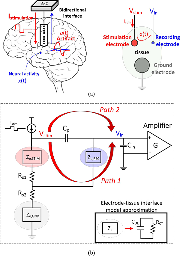
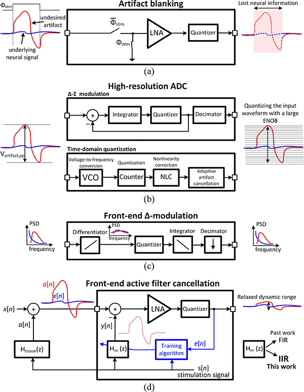
BRAIN-computer interfaces (BCI) have become an integral component in both research and clinical settings [1]–[4]. Responsive neurostimulation (RNS) is an example of such a closed-loop system that monitors the brain activity continuously in patients with epilepsy using 4 recording channels [5]. When the onset of a seizure activity is detected, stimulation pulses are sent to specific regions of the brain to possibly prevent a seizure. For a chronic implantation of these bidirectional systems in patients suffering from neurodegenerative disorders (e.g. Alzheimer’s and Parkinson’s diseases), a customized low-power IC that can communicate bidirectionally with the neurons in the brain is needed [Fig. 1(a)]. This IC should be able to simultaneously stimulate different regions of the brain while amplifying and recording the neural activity through high-density micro-electrode arrays (MEA) [6], [7]. The MEAs incorporate metallic surfaces that are in contact with the biological tissue. The metal-electrolyte interface initiates complex electrochemical reactions. However, it has been shown that such an interface can be modeled with an RC network [refer to the inset in Fig. 1(b)] [8]. A double-layer capacitance (CDL) mimics the formation of an ionic layer next to the exposed metallic surface and a charge-transfer resistance (RCT) models the electron transfer between the metal and the solution. Fig. 1(b) depicts a simplified model of how the delivery of the stimulation current (Istim) into the target tissue may lead to an undesirable artifact voltage. Since the tissue is conductive, the stimulation current that enters the electrode spreads into the medium (Rs1 and Rs2). This creates a voltage profile in the surrounding tissue, which is received by the nearby recording electrode (Path 1). However, the scenario can become more complex when stimulation and recording are performed using shared electronics and electrode arrays. As shown in Fig. 1(b), due to the impedance which naturally exists at the electrode-tissue interface, the stimulation current induces a stimulation voltage (Vstim) at the stimulating electrode. Vstim may leak directly to the input amplifier through the parasitic elements that exist in the system, e.g. via a parasitic capacitance (Cp) across adjacent long wires connecting the stimulation and recording electrodes to the bidirectional interface electronics (Path 2). This artifact voltage may reach a few volts at the location of the stimulation, which can easily saturate the low-noise amplifier (LNA) that is conventionally designed to handle μV-level neural signals [9]–[17]. If a 1 Vpp artifact contaminates a 10 μVp neural signal, the system will need to handle a dynamic range of at least 100 dB, which is equivalent to >16b of effective number of bits (ENOB). Different techniques have been proposed to address this issue, which can be categorized into the front-end and back-end mitigation solutions [18]. The front-end techniques aim to prevent the neural signal distortion by addressing the artifact before quantization. The back-end cancellation tries to restore neural information from the contaminated data by using data reconstruction [19] or component decomposition techniques such as the principle component analysis (PCA) and the independent component analysis (ICA) [20], which are computationally expensive and usually performed off-chip. As a more efficient method, back-end stimulation artifact rejection using adaptive digital filters has been implemented [21], [22]. It is critical to note that without any front-end artifact mitigation, the back-end data processing cannot restore the distorted or lost neural data. A straight-forward front-end mitigation technique is to disconnect the amplifier input when the stimulation current is applied, preventing the artifact to appear at the front-end [23]–[25], as shown in Fig. 2(a). However, the artifact blanking method suffers from slow transient settling due to the low high-pass cutoff frequency of the amplifier. A more severe drawback is the complete loss of the neural data during the stimulator activity, which worsens as the number of the stimulation channels increases. To prevent losing any neural signal, high resolution ADCs [26] can be implemented to accommodate the full range of the artifact voltage, as shown in Fig. 2(b). ΔΣ-modulator front-ends [27]–[29] use a high oversampling ratio (OSR) to achieve the required ENOB, which results in additional power consumption during the decimation and post-processing of the over-sampled data. As an alternative to the voltage-domain quantization, a front-end voltage-controlled oscillator (VCO) can translate the full-scale voltage variations into time-encoded data, which relaxes the analog front-end (AFE) circuitry design by removing the need for voltage amplification [30]–[32]. Since the voltage-to-frequency conversion is a highly nonlinear process, a nonlinearity correction block is needed to compensate for the added distortion. An alternative method to suppress the VCO nonlinearity is to embed the VCO and quantizer in a feedback loop [33]. High resolution ADCs with competitive power consumption (including the decimation circuitry) have been demonstrated mainly for input frequencies up to 500 Hz, which are only suited for recording the local field potentials (LFP) and not the action potentials (AP). However, recording the AP or spikes, which occupy frequencies up to a few kHz, is critical for neuroscientists to understand how neuronal units and populations communicate with each other to function properly (e.g. short-term memory encoding [34]). Scaling these systems to handle a larger input bandwidth significantly adds to the power consumption and system complexity, since the switching frequency required at the front-end quantizer and the back-end digital circuitry for decimation and/or non-linearity correction scales linearly with the maximum bandwidth of the input signal. In another effort to handle a wide input dynamic-range, front-end differentiators and Δ-modulators have been proposed to take advantage of the 1/f1∼3 power spectral density of the neural data [35]–[39]. As Fig. 2(c) shows, Δ-modulation flattens the signal power over the neural signal bandwidth by amplifying the low-power high-frequency components (AP) more than the high-power low-frequency components (LFP). This can relax the dynamic range requirement of the quantizer. The main drawback of this scheme for stimulation artifact cancellation is that the artifacts can have large fundamental and harmonic spectral components in the kHz range [40], which can not be mitigated by front-end Δ-modulation.
Fig. 1.
(a) Conceptual diagram of a bidirectional neural interface and the source of stimulation artifact. (b) A simplified diagram of artifact coupling to to amplifier input (REC: recording, STIM: stimulation, GND: ground).
Fig. 2.
Stimulation artifact front-end mitigation techniques. (a) Artifact blanking. (b) High resolution ADCs. (c) Delta-modulated front-ends. (d) Front-end adaptive filters.
Past in vivo measurements have demonstrated a less than 10% variation in the artifact waveform during a stimulation session [41]. This suggests that a periodic stimulation signal would generate a periodic artifact, implying that the recording system does not necessarily need to quantize the full artifact waveform at every stimulation cycle. If a replica of the artifact waveform is periodically subtracted from the incoming contaminated signal before quantization, the DR requirements of the recording ADC can be significantly reduced. Consequently, adaptive artifact mitigation in the front-end has been proposed, which can potentially provide a flexible, scalable and low-power solution for artifact cancellation in a high-density neural-interface platform. It reduces the dynamic range at the AFE input and enables the use of conventional successive-approximation-register (SAR) ADCs with ENOB <11, while preserving both the LFP and AP neural data [42]–[46]. The concept of the adaptive filtering scheme is shown in Fig. 2(d). When the stimulation signal s[n] is activated, the stimulation current enters the electrode-tissue interface, creating an artifact voltage at the stimulating electrode surface. This artifact voltage is picked up by the recording electrodes as a[n], corrupting the received neural data x[n]. In order to suppress the undesirable large-signal artifact, which can potentially saturate the front-end amplifiers, an on-chip digital filter Hm(z) is used to mimic the response of the electrode-tissue interface. This digital filter generates a replica of the artifact voltage y[n] and applies it to the LNA input, suppressing the artifact waveform at the front-end. The cancellation filter Hm(z) can be realized either with a finite impulse response (FIR) or an infinite impulse response (IIR) configuration. Before choosing the architecture, we should first investigate the possibility of developing a simple model that can mimic the artifact waveform.
II. Modeling the Stimulation Artifact
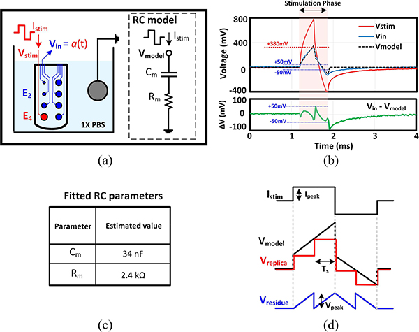
Fig. 3(a) shows the experimental setup that was used for characterizing the artifact voltage. A parylene-based micro-electrode array [47] was used to investigate the challenging case of stimulation and recording from electrodes on a single shank, spaced just 2 mm apart. A biphasic 35 μA stimulation current, with 330 μs per phase, was applied to electrode 4 (E4, with a diameter of 210 μm), while the waveform of electrode 2 (E2, with a diameter of 60 μm) was measured as the target recording site in this example. Fig. 3(b) plots the stimulation voltage and the resultant artifact waveform. Due to the similarity between the waveform of the stimulation and artifact voltages, a simple series RC network (Rm,Cm) was examined as a potential model for the artifact waveform [Fig. 3(a)]. Through computer simulations, the optimized RC parameters that recreated the waveform of the artifact voltage were found [Fig. 3(c)]. The simulated response of the RC model (Vmodel) is plotted in Fig. 3(b). Examining the difference between Vmodel and Vin demonstrates that during the stimulation phase, the model can emulate the artifact with a maximum of 50 mV discrepancy (For 70% of the stimulation time, this discrepancy is less than 20 mV). Hence, in this example, if we could physically create Vmodel and subtract it from Vin before amplification, the dynamic range (DR) that the AFE needs to accommodate reduces from 380 mV to 50 mV, which is a factor of 7 or equivalently 3 bit improvement in the required DR for the AFE+ADC signal path. After the stimulation phase, due to the mismatch between anodic and cathodic currents, there is a residual charge on the stimulation electrode which discharges slowly as can be seen in Fig. 3(b). Charge balancing techniques [48] can be implemented to suppress this slowly decaying waveform, which is beyond the focus of this article.
Fig. 3.
(a) Artifact measurement test bench and proposed RC model. (b) RC model output displayed with the measured stimulation and artifact voltages. (c) Fitted RC model parameters. (d) Stimulation artifact waveform and filter response.
An straightforward way to implement the model is to physically realize Rm and Cm on chip. However, implementing a nF-range capacitance on-chip and copying the stimulation current to regenerate the artifact waveform is not an efficient solution. It may be possible to implement the RC network in the digital domain with a more compact footprint. The transfer function of the RC model can be written as Through a bilinear transformation, by substituting s with (Ts: sampling period), the Z-domain transfer function can be derived as,
| (1) |
where b0 and b1 are functions of Ts, Rm and Cm. Approximating the continuous Vmodel with a discrete-time waveform (Vreplica) introduces residual artifact. The value of Ts should be chosen small enough to reduce the residual artifact voltage [i.e. Vresidue= Vmodel - Vreplica, as shown in Fig. 3(d)] sufficiently below the level that would saturate the front-end LNA. This criterion sets the minimum required sampling speed of the digital filter as a function of the peak stimulation current and the electrode-tissue capacitance,
| (2) |
Assuming Ipeak = 100 μA, Cm = 30 nF, the LNA supply voltage VDD = 1.0 V and the LNA gain G = 25, the upper limit for Ts can be derived as 12 μs.
Past work has implemented adaptive FIR filters to replicate and cancel the artifact waveform at the front-end. However, this topology requires a large number of taps [42] to reproduce the artifact waveform, which can be attributed to the existence of a pole in Hm(z). In high-density MEAs where recording and stimulation electrodes are close, the artifact level may reach a few volts, which is an order of magnitude above the performance limits of the existing FIR schemes [42]–[46]. However, an IIR implementation of the digital filter realizes a pole which can better approximate the electrode response and drastically improve the cancellation performance. The reduced number of coefficients in the IIR implementation carries the following additional advantages: (1) reduced silicon area for filter realization and (2) reduced computational power, both by an order of magnitude as shown in Fig. 4. Here we present an adaptive IIR stimulation artifact canceler; Section III discusses different aspects of the design strategy, section IV describes the system operation, and section V shows the AFE characterization and canceler performance in different scenarios.
Fig. 4.
Block diagram and comparison of the FIR and IIR cancellation filters.
III. System-Level Analysis
Fig. 5(a) shows the simplified configuration of the amplifier chain with the cancellation capacitive DAC (CDAC). An artifact waveform appearing at the amplifier input consists of differential-mode (DM) and common-mode (CM) components [Fig. 5(b)]. Since the cancellation filter injects the artifact replica (y[n]) to the LNA input differentially, the differential component of the artifact is canceled; however, the CM component is not affected, which can deteriorate the AFE linearity by perturbing the device biasing. To quantify the tolerable common-mode artifact, let us consider the front-end of an AFE with the cancellation DAC capacitors (CDAC) connected to the virtual ground, as shown in Fig. 5(b). Assuming that the operational transconductance amplifier (OTA or gm cell) has a low common-mode gain (<1), any input common-mode signal experiences a capacitive division at the virtual ground according to
| (3) |
assuming negligible parasitic capacitance at the OTA input. Considering a conventional inverter-based gm cell, the input common mode range can be given by,
| (4) |
Assuming V DD = 1V, VOV,5 = VOV,6 = 100mV and VGS,1 = VSG,3 = 350mV, the input-common mode range of the OTA can be calculated as 0.45V < Vi,OTA,CM < 0.55V. This sets a limit on the maximum input common-mode range that the amplifier can tolerate as shown below,
| (5) |
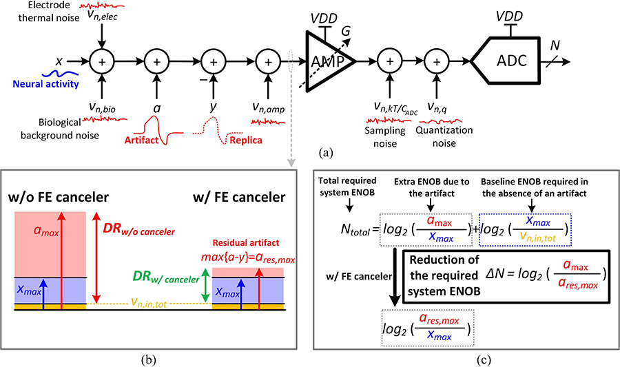
Noise, area and power consumption should also be considered when adding additional circuitry to the front-end. Fig. 6(a) shows the simplified signal flow diagram and noise sources in the system. The total input referred noise can be derived as,
| (6) |
where vn,bio is the biological background noise, vn,elec corresponds to the electrode thermal noise, vn,amp is the input-referred noise of the amplifier, captures the ADC sampling noise, vn,q is the ADC quantization noise and G is the gain of the amplifier. The amplifier noise vn,amp can be derived from the circuitry in Fig. 5,
| (7) |
| (8) |
where γ is the MOSFET noise factor, T is the temperature in Kelvins, k is the Boltzmann constant, BW is the system’s effective bandwidth and gm is the transconductance of M1,2,3,4. Also, the flicker noise is considered negligible compared to the thermal noise, but should be included for a more thorough analysis. Assuming that the devices in the OTA are biased in weak inversion for maximum efficiency, , where I1 is the DC current in each branch of the OTA, n is the subthreshold factor and VT is the thermal voltage. The biological background and electrode noise depends on the electrode and the live tissue conditions, and not the electronics circuitry. Hence, in the following discussion, the focus will be on the noise contribution of the electronics, namely the amplifier and ADC. Assuming CFB1 ≪ C1 (LNA typically has a gain≫1), vn,in,total can be rewritten as,
| (9) |
where CADC is the ADC single-sided sampling capacitance and Δ is the magnitude of the least-significant bit (LSB) of the ADC. The LSB is a function of the ADC full-scale differential voltage (in this case 2VDD) and resolution (N), as given by . Fig. 6(b) shows that without stimulation artifact cancellation, the maximum input the system receives increases from the maximum desired signal (xmax, usually a few mV in the LFP band) to the maximum artifact level (amax, up to a few Volts). Therefore, assuming that the minimum desired signal to be detected is as low as the noise floor, the additional required number of bits imposed by the artifact is . However, if a replica of the artifact (y) is subtracted from the input signal, the swing of the input waveform reduces to the the magnitude of a residual artifact, ares = a − y, which depends on the accuracy of the artifact prediction model. Using such an artifact mitigation approach reduces the required ENOB by , as shown in Fig. 6(c). Therefore, reducing an artifact amplitude from 500 mV to 50 mV at the front-end is equivalent to a 3.3-bit reduction in the required ENOB for the recording system.
Fig. 5.
(a) Simplified block diagram of the front-end configuration. (b) Differential-mode artifact cancellation at the LNA input and common-mode limitation (VCMST: body bias voltage).
Fig. 6.
Noise and dynamic range analysis. (a) Signal flow diagram of the artifact, desired signal and noise. (b) Effect of the front-end (FE) cancellation on the dynamic range (DR). (c) Required DR for the recording system.
On the other hand, the maximum residual artifact limits the maximum gain the AFE can accommodate before saturating the amplifier, as given by . Under these conditions, (9) can be rewritten as,
| (10) |
Equation (10) provides the basis for evaluating the trade-off that exists between the noise floor, ADC resolution, AFE power, CDAC and CADC values (area) and maximum residual artifact. ares,max depends on the accuracy of the training model, and depending on the target setup and experimental conditions, it should be measured early in the system design process. Larger residual artifacts (or equivalently the estimation error) require a higher ENOB and a larger sampling capacitor for the ADC to maintain the noise performance. On the other hand, if the amplifier noise is dominant, even though a larger CDAC provides a higher input CM resilience as suggested by (5), the AFE should consume more power to maintain the target noise level. A larger CDAC would also occupy more chip area. To evaluate the noise performance of the system, let us assume that the system should be resilient to CM artifacts up to 200 mV, which according to (5) requires CDAC = C1. For a target requirement of the area, noise and power consumption of the system, the design parameters should be optimized. In this work, the main focus is on the implementation of the proposed front-end cancellation scheme as a proof-of-concept, which by itself can potentially reduce the burden on the recording system as discussed before. Therefore, the design parameters were chosen based on the conventional front-ends: N = 10, CADC = 2.5pF, V DD = 1V, I1 = 1μA, n = 1.5, γ = 2/3. Following the discussion in section II, ares,max is assumed to be 50 mV. Under these assumptions, the input-referred noise in (10) can be calculated as,
| (11) |
which yields vn,in,total = 28.6μVrms. In this scenario, the ADC quantization noise (28.2 μV) dominates the overall noise performance. Depending on the target application and the minimum signal level to be detected, higher resolution ADCs may be needed to reduce the quantization noise, preferably below the thermal noise of the amplifier. In fact, if an ADC with N-bit resolution is used, by adding the proposed front-end cancellation scheme, which can potentially reduce a 500 mV artifact to 50 mV residual artifact, the input-referred total ENOB accommodated by the system would increase to N+3.3 bits.
IV. Circuit Implementation
A. System Architecture
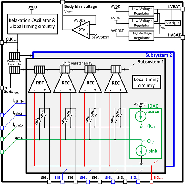
Fig. 7 shows the implemented SoC which consists of two identical subsystems, each having four recording front-ends (REC) and a biphasic neural stimulator 7b-current DAC (IDAC). A front-end switching matrix (SWi−, SWi+, i= 0–7) can reconfigure the stimulator connection to any of the recording electrodes on-the-fly. This enables reusing the electrodes for both recording and stimulation, which can potentially prevent additional electrode routing and placement in the brain and reduce the damage to the tissue. The digitized outputs of all the 8 recording channels are serialized, packetized and transmitted via 2 serial lines (Serialout and CLKout). Fixed preamble and postamble bit patterns are added to the bit-stream to flag the start and end of the consecutive data packets. An on-chip 25 MHz RC digital relaxation oscillator generates a tunable core clock for the chip, which is used to create proper timing for the operation of the SAR ADC, stimulation circuitry, LMS-IIR filter and data transmission. Low-dropout regulators combined with the bandgap voltage circuitry generate 3 main supplies for proper chip operation, namely the core analog and digital supply voltages AVDD and DVDD (both equal to 1 V) in addition to the 3 V supply voltage AVDDST. Since the stimulation IDAC operates within 3 V and 0 V limits, the tissue should be biased to half this range to achieve the maximum headroom for source and sink transistors in the IDAC. Hence, a unity-gain buffer is designed to set the body voltage at VCMST = 1.5 V, which is half AVDDST. IDAC is designed with 7-bit binary-weighted PMOS and NMOS current sources, providing up to 127 μA maximum current with 1 μA resolution.
Fig. 7.
Neural interface SoC block diagram.
B. Recording Channel Circuitry
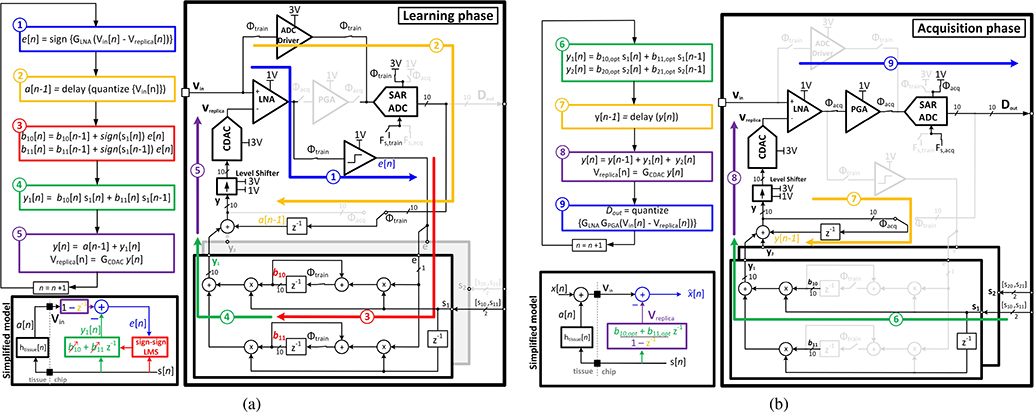
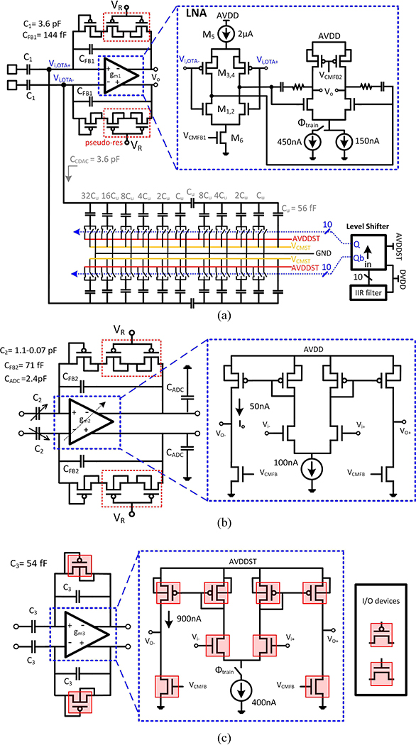
The detailed block diagram of the REC block is shown in Fig. 9. All blocks are fully differential; but, for simplicity, the single-ended version is depicted. Each REC block incorporates a front-end 2-stage LNA, followed by a programmable gain amplifier (PGA). As shown in Fig. 8(a), the first stage of the LNA has an inverter-based topology to provide a power-efficient low-noise front-end. It is followed by a Miller-compensated active-load differential pair with a switchable tail current. To save the chip area, the LNA is reused during the training phase to amplify the difference between the artifact and its replica, which requires a faster settling in this phase. Hence, the LNA can be switched between regular-bandwidth and high-bandwidth modes. The PGA provides a tunable gain and also acts as an anti-aliasing filter for the ADC, by limiting the signal bandwidth to about 10 kHz to reject the out-of-band noise and distortions [Fig. 8(b)]. The low-pass corner of the PGA is determined by the mid-band gain , transconductance of the OTA (gm2), and the capacitive load of the SAR ADC (CADC) as . The transconductance is tunable to meet the minimum bandwidth requirement for different gain settings. The output stage of gm2 accommodates a wide-swing differential output during the signal acquisition. To ensure that the PGA can maintain the maximum output swing (VFS= 1V) in the available tracking time of the ADC, which is about 70% of the sampling period in this design (Ts=50μs), the DC current of its output stage (Io) should be at least , which requires Io>34 nA. Since the artifact voltage may appear with different amplitudes at the input of each recording channel depending on the distance of the electrode to the stimulation site, each recording channel is equipped with an independent adaptive cancellation filter. A 10b binary-weighted split-array capacitive DAC (CDAC) converts the digital filter output to a differential artifact replica, which is applied to the LNA input terminals, as illustrated in Fig. 8(a). Since the digital blocks operate at 1 V, level-shifters are needed to provide 3 V control signals for driving the switches in the CDAC. The CDAC output capacitance at the virtual ground terminals of the LNA degrades the input-referred noise. Therefore, during the acquisition phase and in the absence of any stimulation signal, the CDAC capacitors can be open-circuited to improve the AFE noise performance.
Fig. 9.
Front-end IIR LMS filter principle of operation. (a) Learning phase. (b) Acquisition phase. The disabled blocks are shown in a light gray color.
Fig. 8.
Detailed circuitry of the AFE. (a) LNA and CDAC configuration (b) PGA (c) ADC driver.
C. Operation of the AFE with the Adaptive IIR Filter
We used the simplified transfer function of the electrode-tissue interface as our system model to be trained: . The implemented adaptive algorithm adjusts the filter coefficients using the equation-error approach [49]. Such configuration guarantees global convergence as with an adaptive FIR filter.
1). Learning (Training) Phase:
During the training phase the PGA is disconnected, as shown in Fig. 9(a). The input voltage Vin is directly buffered to the ADC through the ADC driver [Fig. 8(c)], generating the quantized artifact signal a[n]. The unity-gain ADC driver is used to isolate the recording electrodes from the switching transients during the sampling period of the SAR ADC operation. The driver also removes the input common-mode component and provides a differential waveform at the ADC input. In this phase, the ADC operates with Vreference = 3 V to accommodate the high-voltage artifact. Its sampling rate should match the clock frequency of the digital filter and the CDAC switching speed, which is set to Fs,train = 78.4 kHz. This high sampling rate reduces the residual artifact at the AFE input below the saturation limit of the amplifier, as was derived in (2). Moreover, the chosen Fs,train reduces the quantization noise power injected by the CDAC in the ADC’s Nyquist bandwidth (f < 10 kHz) during the acquisition phase. To accommodate a high slew-rate during comparison, the LNA is switched to the high-bandwidth mode. It operates as a pre-amplifier for the equation-error comparator, which generates the 1-bit equation-error e[n] based on the comparison between Vin and Vreplica. To simplify the hardware implementation of the LMS algorithm, a sign-sign scheme is realized [42], [43]. For each stimulator, the sign of each stimulation signal is represented with 2 bits ([s10, s11] for stimulator 1 and [s20, s21] for stimulator 2), to accommodate 3 possibilities of anodic (positive), cathodic (negative) and disabled current stimulation. All the mathematical operations are performed in a 2’s complement system to accommodate negative numbers. To enable simultaneous cancellation of 2 independent stimulation signals, each channel has 2 pairs of 10b coefficients [b10, b11] and [b20, b21], which are independently adapted to their corresponding stimulation signals s1[n] and s2[n]. In a general scheme with N stimulators, the coefficients are updated according to,
| (12) |
where j is the stimulator index (j= 1…N). In this implementation, the adaptation constant μ is set to 1 for hardware simplification. It should be emphasized that for a guaranteed coefficient convergence, the coefficients corresponding to each stimulator need to be trained separately, when all other stimulators are disabled. However, during the acquisition phase the stimulators can be activated simultaneously and there is no timing constraint. In the example shown in Fig. 9(a), [b10, b11] are being adapted to [s10, s11], while the second stimulator is disabled, [s20, s21]= 0. The artifact replica y[n] at each cycle is estimated by the summation of the delayed quantized artifact a[n − 1] and the digital filter output, according to,
| (13) |
Since the adaptation constant is fixed, the training time scales linearly with the artifact peak-to-peak voltage, at a rate of 20 mVpp per stimulation pulse applied to a resistive load. For instance, for a 200 mVpp artifact, 10 stimulation cycles are needed to train the filter coefficients.
2). Acquisition Phase:
When the training phase is complete and the filter coefficients are adapted to their corresponding stimulation signals, the system enters the acquisition phase [Fig. 9(b)]. The IIR filter generates the artifact replica waveform in response to the stimulation signals, given by
| (14) |
where [bj0,opt, bj1,opt] are the converged filter coefficients. The LNA is switched back to the regular-bandwidth mode and the PGA is switched into the amplification chain, connecting the LNA output to the ADC. The equation-error comparator and the ADC driver are disabled and disconnected from the rest of the circuitry. In this phase, the sampling rate of the SAR ADC reduces to Fs,acq = 19.6 kHz, which is sufficient to accommodate the neural signal bandwidth, while preventing any excess power consumption for digitization and data transmission. The ADC also operates with Vreference = 1 V, which is sufficient to accommodate the amplified neural signal and the residual stimulation artifact.
V. Measurements
A. System Performance
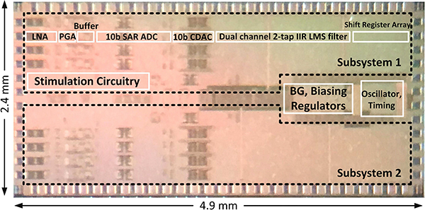
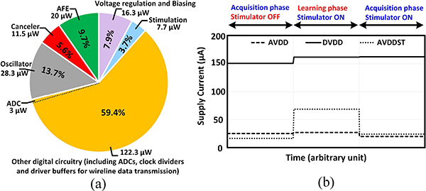
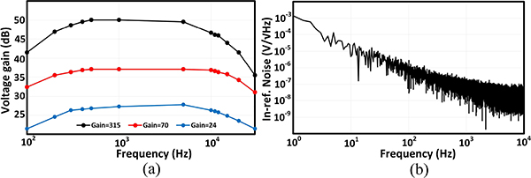
The 0.18μm CMOS SoC microphotograph is shown in Fig. 10. The chip occupies 11.4 mm2 of area and consumes a total of 206 μW of power when all the recording channels are in the acquisition mode and one stimulator is delivering a biphasic 40 μA peak current with cathodic and anodic pulse widths of 300 μs and a period of 2 ms. The power consumption breakdown is shown in Fig. 11(a). The current consumption of different supply voltages in different operation modes is also plotted in Fig. 11(b). Fig. 12 shows the measured frequency response of the AFE (LNA in the regular-bandwidth mode+PGA) and its input-referred noise spectral density. The AFE achieves a 9 kHz bandwidth, an integrated input-referred noise of 6.2 μVrms and a common-mode-rejection-ratio (CMRR, defined as the ratio of the differential gain to the CM-to-differential conversion gain) of 43.2 dB at the maximum differential gain of 50.0 dB. Analysis and simulations suggest that an imbalance between the parasitic capacitances at the virtual ground nodes of the LNA dictates the maximum CMRR in our design. A more careful layout of the LNA with a better routing symmetry should achieve a higher CMRR. The AFE was originally designed to achieve sub-Hz high-pass cutoff frequency by using switchable pseudo-resistors around the gm cells [refer to Fig. 8(a)]. However, the n-well to p-substrate leakage current disrupted the feedback DC path around the LNA and PGA when the pseudo-resistors were enabled (VR= 1 V). For proper DC biasing, the pseudo-resistors had to be shorted (VR= 0 V), which resulted in a high-pass cutoff frequency of 200 Hz (sufficient to record the AP but not the LFP). The increase in the high-pass corner also contributed to the degradation of the input-referred noise. For future designs, especially those with TΩ-range effective resistances, substrate leakage compensation techniques should be implemented [50]. The dynamic linearity performance of a stand-alone SAR ADC was measured in 2 different settings corresponding to the different modes of operation: (1) Sampling speed Fs = Fs,train and Vreference = 3 V, (2) Fs = Fs,acq and Vreference = 1 V. At the Nyquist frequency, the ADC maintains an SFDR and ENOB of 62 dB and 8.6b for Fs,acq and 56 dB and 7.6b for Fs,train. The stand-alone CDAC could not be characterized with the available setup; however, the parasitic extracted simulations showed that it maintained a spurious-free dynamic range (SFDR) of 68 dBFS for a 10 kHz output signal.
Fig. 10.
Die microphotograph.
Fig. 11.
(a) Chip total power consumption breakdown. (b) Supply voltage currents in different operation modes.
Fig. 12.
(a) AFE frequency response. (b) AFE input-referred noise for the maximum gain setting.
B. Stimulation Artifact Canceler Performance
1). Single Channel Stimulation:
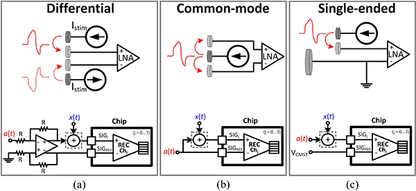
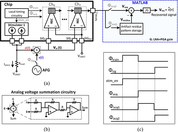
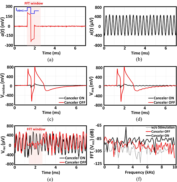
Depending on the relative location of stimulation and recording sites in the tissue, the stimulation artifact can couple into the amplifier input in 3 different modes: differential, common-mode and single-ended, as demonstrated in Fig. 13. In the following benchtop characterization, an off-chip circuitry was implemented to artificially generate each mode, as shown in Fig. 13. The functionality of the adaptive IIR filter was first investigated in the presence of single-ended artifact generated from a single-channel stimulation, as shown in Fig. 14(a). An arbitrary function generator (AFG) generated a 400 μVp, 3.05 kHz sinusoidal signal x(t) (mimicking the neural signal), which was applied to all the recording channels with the AFE gain programmed to 27.6 dB. With this setting, the signal-to-noise ratio (SNR) of the recorded signal is about 10 dB, when averaged across channels. In the training phase, the AFG was disconnected and the stimulation signal (stim_en) enabled stimulator 1 to apply a balanced biphasic 19 μA stimulation current, with 330 μs duration per phase and repetition rate of 140 Hz, into an off-chip 9.5 kΩ resistor to generate a biphasic artifact waveform. The generated artifact waveform a(t) was fed to the recording channels and all the 8 REC blocks were allowed sufficient time for training their IIR filter coefficients during Φtrain. At the beginning of the acquisition phase during Φacq1, the chip output, which carried the residual artifact Vresidue, was stored in MATLAB. During Φacq2, which was the final phase of the testing cycle, the AFG and stimulator 1 were both active and x(t) was summed with a(t) artificially using an off-chip op-amp circuitry shown in Fig. 14(b). The stored Vresidue was subtracted from the chip output (Vacq) and divided by the system AFE gain in this phase to recover the input-referred sinusoidal signal (Vrec). The resultant artifact and input sinusoidal signals are depicted in Fig. 15(a)–(b). The goal of the experiment was to recover the 3.05 kHz signal with minimal distortion, while maintaining the signal amplitude. The functionality and efficacy of the implemented front-end adaptive cancellation was investigated by comparing the recovered signal when the canceler IIR filter was enabled (canceler ON) versus when the filter was disabled (canceler OFF), while the back-end cancellation remained active in both cases. Fig. 15(c) demonstrates that the front-end IIR filter is mitigating the artifact, resulting in a minimal Vresidue. The ADC output during the acquisition phase shows a reduced artifact on top of the sinusoidal signal [Fig. 15(d)]. The recovered signal in Fig. 15(e) shows that without the front-end canceler, the sinusoidal waveform is completely lost in the background noise during the stimulation phase. A time window of 32 samples, equivalent to 1.6 ms starting from the onset of the stimulation signal, was chosen for spectral analysis. By comparing the Fourier transform of the recovered signals in Fig. 15(f), a complete recovery of the fundamental tone was observed when the IIR filter was active. When the front-end canceler is off, the large-swing artifact saturates the LNA, which results in increased distortion and failure to detect any underlying signal. It is important to note that the selected 1.6 ms duration for the time window is about the average duration of a neural spike. Hence, without the canceler, any neural spike which is coincident with the stimulation signal could be easily lost in this scenario.
Fig. 13.
Different modes of stimulation artifact coupling into the amplifier input (a) Differential (b) Common-mode (c) Single-ended. The off-chip circuitry that generates each mode is also included.
Fig. 14.
(a) Measurement setup for testing the performance of the artifact canceler. (b) Off-chip voltage summation circuitry. (c) Timing diagram of the successive operation cycles and phases.
Fig. 15.
(a) Stimulation artifact. (b) Single-tone input signal. (c) Residual artifact waveform recorded during Φacq1. (d) Recorded signal contaminated with the residual artifact during Φacq2. (e) The recovered amplified input signal (The time window that the FFT is performed on is shown with a red rectangle). (f) Frequency spectrum of the recovered signal. The FFT of the recorded signal in the absence of the stimulation signal is also plotted. The representative waveforms are shown for channel 0.
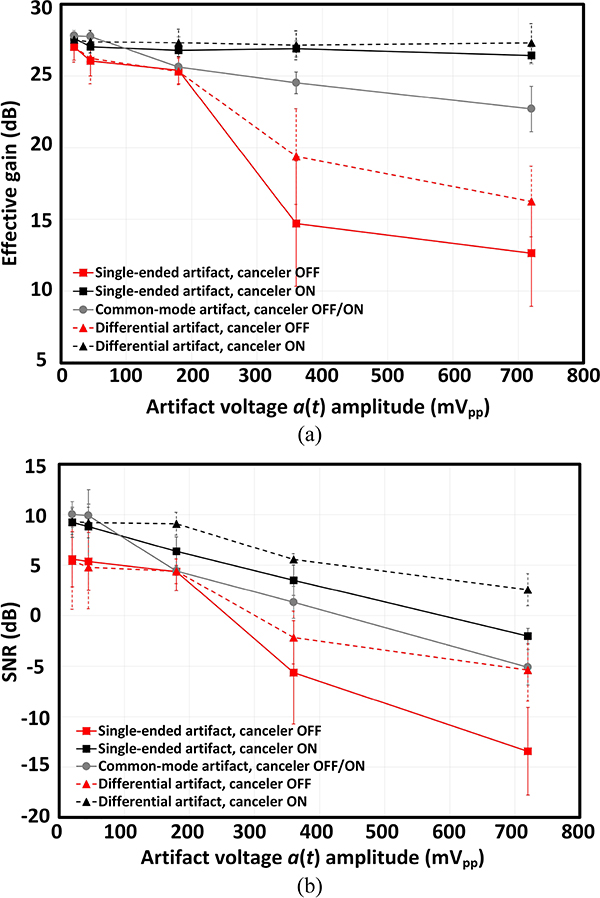
The same characterization steps were performed for differential and common-mode stimulation artifacts as well. To evaluate the efficacy of the proposed cancellation scheme in suppressing different artifact intensities, the stimulation current was swept from 1 μA to 35 μA, while the load impedance was an off-chip 9.5 kΩ resistor. Figure. 16(a) plots the measured system effective gain (defined as the ratio of the intensity of the recovered fundamental tone to the input signal) as a function of the artifact peak-to-peak voltage. To quantify the signal distortion and noise introduced by the artifact, the SNR was also measured using the frequency spectrum of the recovered signal, which is shown in Fig. 16(b). Both the effective gain and SNR metrics were measured for all the 8 channels and the average values with ±1σ variation across the channels are shown in Figure. 16. For differential and single-ended modes, at medium-level artifact amplitudes (< 200 mVpp), the effective gain of the system is slightly improved (< 2 dB) when the front-end canceler is enabled. SNR also shows similar behavior with an improvement of < 4 dB for small artifact amplitudes. As the artifact level increases to about 400 mVpp, for both the single-ended and differential modes, the amplifier is significantly saturated and the effective gain drastically drops by about 10 and 6 dB, respectively. However, enabling the canceler restores the effective gain and prevents signal attenuation. Moreover, the front-end canceler also improved the SNR by more than 8 dB for artifact amplitudes above 200 mVpp. Assuming a 0-dB SNR is the limit for a likely detection of spikes [51], these measurements suggests that the canceler can recover 400 μV high-frequency signals in the presence of 600 mVpp single-ended and > 700 mVpp differential artifacts. Preserving the gain for large artifacts (> 700 mVpp) also suggests that the canceler is suppressing the artifact and preventing the saturation of the amplifier. In this region, the SNR degradation can be attributed to the increased noise and distortion introduced by the cancellation CDAC. All these measurements were performed under the challenging scenario of exact alignment of the artifact with the signal. As discussed earlier, in the current implementation, the cancellation filter cannot capture and cancel the common-mode artifact. The only suppression that occurs is the capacitive division at the LNA input. Common-mode artifacts larger than 100 mVpp degrades both the gain and SNR. Any CM stimulation artifact converted to a differential mode due the low CMRR of the front-end, will be automatically included in the pattern stored for the residual artifact in the back-end during the acquisition of the residual artifact [Φacq1 in Fig. 14(c)]. During the acquisition phase, this stored waveform, which includes both the residual differential artifact and the CM-to-differential converted component of the stimulation artifact, is subtracted from the recorded signal and cancels the CM-to-differential converted artifact.
Fig. 16.
(a) Effective gain and (b) SNR as a function of the input artifact peak-to-peak voltage, measured for single-ended, differential and common-mode artifact waveforms. The error-bars show ±1σ variation across the 8 recording channels.
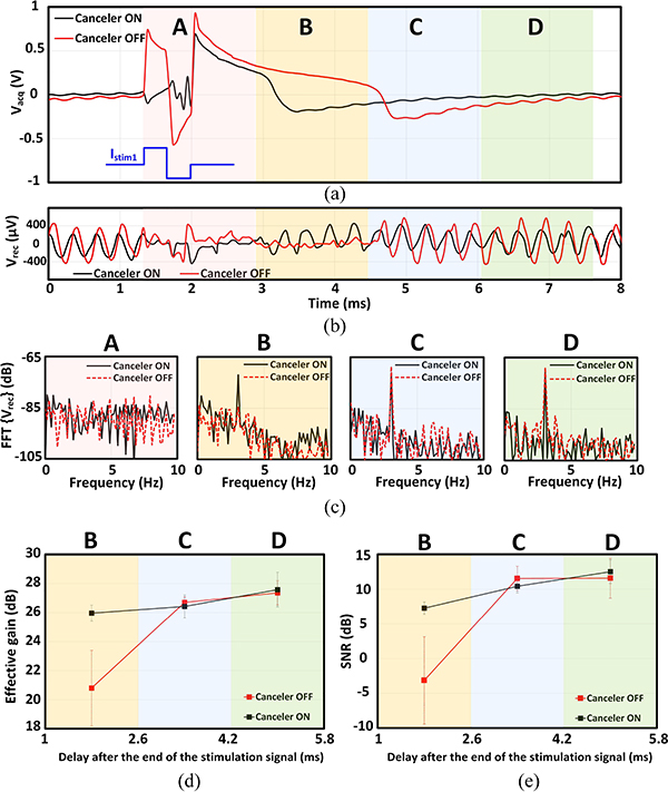
In a closed-loop neural interface, recording an evoked potential is critical since it carries information about the response of the neuronal network to the stimulation pulse. An evoked neural response can occur as early as 1 ms following the stimulus [52]. Therefore, it becomes critical for the front-end amplifier to recover from saturation and restore its linearity soon after the stimulation phase. To investigate the canceler’s performance in such scenarios, a 2.5 Vpp artifact was emulated (30 μA stimulation current delivered to a 41 kΩ resistor) and applied to the recording channel inputs in a single-ended configuration. The acquired waveform at the ADC output and the recovered signals are shown in Fig. 17(a–b). It can be observed that the amplifier recovery from saturation happens almost two times faster when the canceler is active. Fourier transform of sliding time windows of the recovered signals also suggest that during window B, the amplifier is still recovering from a deep saturation state in the absence of the front-end cancellation [Fig. 17(c)]. In the same time window, the canceler has recovered both the effective gain and SNR, as shown in Fig. 17(d–e). This suggests that if a neural spike happens just after the stimulation signal, without the front-end cancellation, it can go undetected.
Fig. 17.
Effect of the canceler on the amplifier recovery time from saturation due to a 2.5 Vpp artifact (a) Recorded signal contaminated with the residual artifact (Sliding time windows are labeled as A-D). (b) Recovered signal. (c) Frequency spectrum of the recovered signal in different time windows. (d) Effective gain and (e) SNR measured in different time windows following the stimulation event.
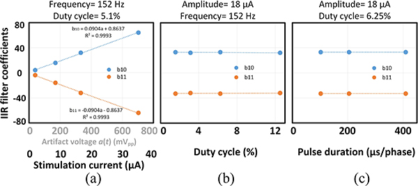
The dependence of the IIR filter coefficients on different stimulation parameters was also studied using the test bench in Fig. 14(a). Fig. 18(a) shows a linear relationship between the adapted filter coefficients and the artifact amplitude, as is suggested by (13). On the other hand, the coefficients have no significant dependence on the stimulation current duty cycle and pulse width, as can be observed in Fig. 18(b)–(c). Since the IIR filter is based upon the empirical model in (1), it resembles an LTI RC network and is therefore independent of the timing properties of the applied balanced biphasic stimulation signal.
Fig. 18.
Dependence of the IIR filter coefficients on the stimulation signal parameters. (a) Amplitude (b) Duty cycle (c) Pulse width.
2). Dual Channel Stimulation:
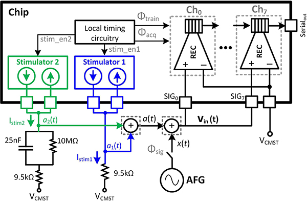
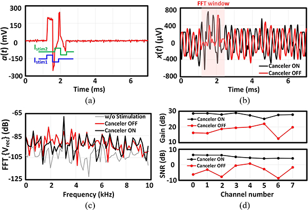
In a high-density neural interface platform, concurrent multi-channel neural stimulation is inevitable in order to investigate how neuronal populations respond to timing differences of such stimuli and map the brain networks in more detail [53]. The past implementations of the adaptive-filter techniques for artifact mitigation [42], [43] were designed to train the filter coefficients to only 1 independent stimulation channel. To demonstrate cancellation of an artifact due to the simultaneous operation of independent stimulation channels, the 2 on-chip stimulators were activated and programmed in such a way that their output currents overlap in time. Stimulator 1 was connected to an RC load and stimulator 2 was tied to a resistive load. The 2 artifacts and a sinusoidal signal were summed off-chip, and were applied to all the 8 recording inputs as shown in Fig. 19. The stimulation currents (Istim1=19 μA and Istim2=10 μA, with 330 μs pulse width) and the resultant artifact are shown in Fig. 20(a). The recovered signal and its Fourier transform are shown in Fig. 20(b) and (c) respectively. The effective gain increased by more than 10 dB when the front-end canceler was activated, suggesting that the canceler was able to keep the AFE in its linear region of operation. Fig. 20(d) shows the effective gain and SNR for the 8 recording channels. The average effective gain was boosted from 18.1 to 27.6 dB. The SNR was also improved from −3.8 to 5.0 dB in average.
Fig. 19.
Test bench for measuring the cancellation performance in the presence of 2 overlapping stimulation signals.
Fig. 20.
(a) Stimulation currents shown on top of the resultant artifact waveform. (b) The recovered amplified input signal (shown for channel 0). (c) Frequency spectrum of the recovered signal. (d) Effective gain and SNR measurement of the recovered signal across different channels.
3). In Vitro Measurements:
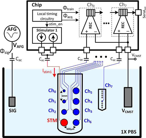
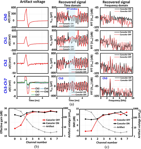
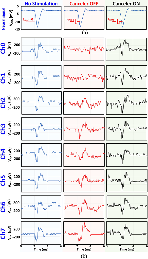
Fig. 21 shows the in vitro measurement setup for testing the performance of the artifact canceler in 1x phosphate-buffered saline (PBS), which can mimic the brain tissue electrical properties. A metallic wire with <1 mm exposed tip was inserted in the solution for injecting the desired signal into the solution (a single tone at 3.05 kHz in the first experiment and a pre-recorded neural waveform in the second experiment). The solution was biased to VCMST via another piece of wire with a few cm of exposed tip. Two sets of flexible parylene-based micro-electrode arrays (MEA) with platinum disc electrodes [47], [54], [55] were used to interface the 8 recording channels with the solution. The microelectrodes had different exposed diameters ranging from 30 to 160 μm. A biphasic 35 μA stimulation current with 330 μs pulse width was injected into the solution via the largest electrode (diameter=210 μm). The artifact waveforms received at different electrodes are shown in Fig. 22(a). A counter-intuitive observation is that channel 0, which is farther away from the stimulation electrode compared to channel 2, experiences a larger artifact. This suggests that, as we mentioned earlier, the artifact coupling mechanisms and pathways are not limited to the solution and tissue itself, but they may arise from the hardware and device properties. The recovered signal and their corresponding frequency spectrum are also shown in Fig. 22(a). For channels 0 and 1 which experience the largest artifacts, the cancellation scheme recovered the underlying signal, with 10 dB improvements in both gain and SNR, as shown in Fig. 22(b–c). As the amplitude of the artifact reduces below 10 mVpp, which is the case for channels 3–7, the amplifier is not saturated with the artifact and the cancellation circuitry has negligible effect on the system performance.
Fig. 21.
In vitro measurement setup for testing the performance of the artifact canceler in 1x PBS. The ac-coupling capacitance Cac= 220nF prevents any DC leakage current through the electrodes, which can potentially deteriorate the electrode performance or even result in its failure. 2 microelectrode arrays were used in this testbench to investigate the artifact coupling in different configurations.
Fig. 22.
Performance of the canceler on a single-tone signal in vitro. (a) Stimulation artifact waveform, recovered signal and its frequency spectrum cross different channels. (b) Effective gain and (c) SNR across different channels. The input artifact amplitude is also shown for each electrode.
Finally, pre-recorded neural spikes were generated and injected into the solution, without changing the existing test bench. Therefore, the artifact waveforms are the same as those shown in Fig. 22(a). The output of the function generator and the overlapping stimulation current is shown in Fig. 23(a). Similar to the single-tone experiment, for channels 0 and 1 the neural signal is lost due to the amplifier saturation, as shown in Fig. 23(b). However, the cancellation filter can recover the neural spike in these channels, which experience the largest artifact levels (up to a 900 mVpp artifact).
Fig. 23.
Performance of the canceler on a pre-recorded neural signal in vitro. (a) The neural signal generated by a function generator. The timing of the stimulation current is also shown. (b) Recovered signal across different channels in 3 conditions: stimulation OFF, stimulation ON + canceler OFF, stimulation ON + canceler ON. The test bench and the artifact levels are the same as the in vitro single-tone test.
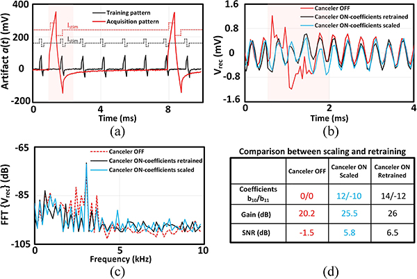
Table I compares the performance of the chip with the state-of-the-art bidirectional neural interfaces. Since the performance of the artifact cancellation depends on a diverse set of experimental conditions such as the stimulation parameters (current intensity, pulse duration and frequency, charge balancing, etc), the electrode impedance, hardware setup and the time window that the spectral analysis is performed, it may be hard to provide a fair comparison between different architectures solely based on their maximum peak-to-peak artifact level handling. Nonetheless, with the presented measurement setup and conditions, the implemented SoC suppresses stimulation artifacts with amplitudes measured up to 700 mVpp, while maintaining competitive noise and power performance. About half of the area of the recording channels is occupied with the digital circuitry, which is all designed and laid out manually. Implementation in a more advanced node and utilizing an automated logic synthesis tool can significantly shrink the area of the digital blocks and routing. Moreover, for an area-optimized design, multiplexing ADCs between channels should be considered. In fact, it may be possible to integrate the cancellation technique discussed here in a fully digital front-end, following the trends suggested in [56]. The 2-tap IIR filter implementation demonstrated in this work can potentially reduce the silicon area needed for storing the filter coefficients, compared to an FIR implementation with 30 or more taps. In a scaled-up system with N recording and M stimulation channels, the proposed scheme requires storing 2MN IIR digital coefficients, which can be conveniently accommodated by the technology scaling. All the recording channels can be trained simultaneously with respect to each stimulation channel, which adds up to a total training time of , where fstim is the repetition frequency of the stimulation current waveform (cycles/s), Rm is the series resistance in the empirical model in Fig. 3(a), and Istim is the stimulation current. If the stimulation artifact shows an LTI response in the target in vivo environment [41], the coefficients can be trained with a scaled-down stimulation current to prevent an undesirable neural response. Moreover, the decreased stimulation intensity carries an additional advantage of reducing the training time. During the learning phase, the frequency of the stimulation signal can also be increased to further shorten the training time. During the acquisition phase, the coefficients should be linearly scaled up with the same ratio as the stimulation currents are scaled [Fig. 18(a)], and the stimulation pattern can be tuned to the desired duty cycle and pulse duration without the need to retrain the filter coefficients [Fig. 18(b)–(c)]. This was verified experimentally in the same in vitro setup as before (Fig. 21) but with a larger ground electrode. The recording channels were initially trained to a stimulation current of 20 μA with a pulse width of 100 μs applied at a rate of 1.22 kHz. In the acquisition phase, the stimulation current was doubled to 40 μA, while the pulse width and frequency were tuned to 400 μs and 152 Hz respectively, as demonstrated in Fig. 24(a). To test the scalability of the canceler as was discussed before, the trained coefficients were multiplied by 2 and the performance of the artifact cancellation to recover a single-tone signal was measured [Fig. 24(b)–(c)]. The response of the canceler directly trained to the scaled-up current was also measured for comparison. Comparing the gain and SNR of the recovered signal in Fig. 24(d) shows that a linear scaling of the filter coefficients is sufficient to cancel the artifact generated by a stimulation current with different amplitude, pulse duration and duty cycle. This suggests that the stimulation parameters can be tuned on-the-fly without the need to retrain the filter coefficients of the canceler.
TABLE I.
Performance Summary and Comparison with the State-of-the-art Bidirectional Neural Interfaces
| This work | [28] VLSI’ 17 | [39] JSSC’ 20 | [42] SSCL’ 18 | [43] JSSC’ 16 | [32] TBCAS’ 18 | [17] VLSI’ 16 | [38] VLSI’ 17 | [24] JSSC” 6 | [15] JSSC’ 18 | |
|---|---|---|---|---|---|---|---|---|---|---|
| Technology (nm) | 180 | 180 HV | 130 | 65 | 180 | 40/HV 180a | 180 | 65 | 180 | 130 |
| Supply voltage (V) | 1, 3 | 1, 3∼12 | 0.6, 1.2, 3.3 | 1 | - | 0.6, 1.2, 1.8, ±5 | 0.8, 3.3 | 0.5, 2.5 | 1.8, 2, 3∼12 | 1.2, 3.3 |
| IRNb (μVrms) | 6.2c/11d,e | 1.6 | 1.6 | 7.5c/8.2d | 3.05 | 2.2 | 5.9f | 2.78 | 2.09 | 12.0 |
| Signal BW (Hz) | 200 g -9k | DC-500 | 1–500 | 10–8.3k | 1–2k | 1–250 | 17–1.65k | 1–1k | 0.59–117 | 0.5–10k |
| Voltage gain (dB) | 27.6–50.0 | NA | NA | 45–65 | 40–60 | NA | 42 | NA | 50–70 | 6–69.5 |
| ADC res./ENOB(b) | 10/8.6 | 15/10.2 | 12/11.3 | 10/- | 10/- | NA/12.8 | 8/- | 14/- | 10/7.8i | 10/- |
| THDj | 0.9% 2mVpp,in 1kHz 50dB | 0.7% 0–1Vpp,in 60Hz | - | 0.4% 1.2mVpp,in 1kHz 65dB | - | 0.009k% 0–1Vpp,in 203Hz | - | - | 0.4i% 8.9mVpp,in 97Hz 50dB | 0.89% 20mVpp,in 10kHz 54dB |
| AFE power/Ch(μW) | 2.5 | NA | NA | 1.8 | 0.24 | NA | 0.8 | 2.98i | 3.75 | 25.2 |
| ADC power/Ch(μW) | 0.38 | 8.0 | 1.7 | - | 0.09 | 8.2 | - | - | - | 0.88 |
| Canc. power/Ch(μW) | 1.42 | NA | NA | 0.9 | - | NA | NA | - | NA | NA |
| Rec. area/Ch (mm2) | 0.66 | - | 0.023 | 0.18 | 0.17 | 0.12 | 0.04 | 0.15 | 0.56 | 0.1h |
| # Rec front-ends / Stimulation cores | 8 / 2 | 64 / 4 | 32 / 32 | 64 / 2 | 8 / 4 | 32 / 8 | 16 / 1 | 1 | 16 / 16 | 1024 / 64 |
| # Artifact cancelers | 8 | 0 | 0 | 8 | 8 | 4 | 0 | 1 | 0 | 0 |
| Artifact cancellation method | FE filter | NA | NA | FE filter | FE filter | BE filter | NA | FE template subtraction | - | - |
| # Filter taps, type and learning algorithm | 2, IIR, sign-sign LMS | NA | NA | 32, FIR, sign-sign LMS | 8, FIR, sign-sign LMS | 16, FIR, normalized LMS | NA | NA | NA | NA |
| Max # uncorrelated stimulation artifacts mitigated by each canceler | 2 | NA | NA | 1 | 1 | 1 | NA | 1 | NA | NA |
| Die size (mm2) | 11.76 | 11.52 | 1.0h,l | 5.14 | 1.74l | 9.88/16.43a | 1.1l | - | 25.0 | 192m |
AFE: LNA+PGA, FE: front-end, BE: back-end
NA: Not applicable
-: Not reported
Separate neural recording and stimulation chips in different technologies were fabricated.
Integrated input referred noise measured for the reported bandwidth.
Standalone AFE w/o the front-end CDAC.
w/ the front-end CDAC.
AFE (max gain setting)+ADC quantization noise.
Measured for 10Hz-10kHz.
The high-pass corner was limited because the pseudo-resistors in the amplifier had to be shorted to prevent any disruption in the biasing due to the substrate DC leakage currents.
Estimated.
AFE+ADC.
THD measured for the given single-tone input amplitude, frequency and AFE gain.
Reported HD3, the design uses a nonlinearity correction block.
Active area (excluding pads).
Includes 16k electrode sites and active pixels.
Fig. 24.
Scalability of the IIR filter output in response to stimulation with different parameters in vitro. (a) Stimulation current and artifact during training and acquisition. (b) Recovered signal in 3 conditions: canceler OFF, canceler ON + filter retraining, canceler ON + coefficient scaling. The FFT window is highlighted with a shadow. (c) Frequency spectrum of the recovered signal. (d) Performance summary of the artifact cancellation scheme. The representative plots are from channel 0.
VI. Conclusion
A multi-channel bidirectional neural interface with an adaptive stimulation artifact canceler was implemented in a 180-nm CMOS process. The fabricated SoC demonstrated a 2-tap IIR filter, which was trained with a sign-sign LMS algorithm and could extend the dynamic range of the existing neural recording front-ends by accommodating stimulation artifacts up to 700 mVpp while retaining competitive noise and power performance. The canceler could also reduce the recovery time of a saturated front-end amplifier from a 2.5 Vpp artifact by a factor of 2, which allows for the detection of a fast evoked potential. The implemented front-end canceler could mitigate up to 2 concurrent and independent stimulation artifacts appearing on all the 8 recording channels. The IIR implementation of the active filter significantly reduced the required number of filter coefficients compared to an FIR filter, which in a high-density neural interface, can potentially lead to a substantial decrease in the computational power consumption and chip area for local storage of the filter coefficients. Moreover, the IIR filter coefficients are independent of the timing properties of the stimulation current, while they scale linearly with the stimulation amplitude. This allows for the on-the-fly tuning of the stimulation waveform without the need to retrain the filter coefficients.
Acknowledgment
The authors would like to thank Prof. Ellis Meng, Xuechun Wang and Eugene Yoon for providing the parylene microelectrode arrays, and Prof. Dong Song and Huijing Xu for providing the in vivo neural recordings. They would also like to thank Prof. Ellis Meng, Prof. Dong Song, Prof. James Weiland, Prof. Gerald Loeb and their research group members for technical comments.
This work was partially supported by the NSF under award number 1343193 and the NIH under project number 5U01NS099703-03.
Biography
 Aria Samiei received the B.S. degree in electrical engineering from the Sharif University of Technology, Tehran, Iran, in 2013. He is currently pursuing the Ph.D. degree in electrical engineering at University of Southern California, Los Angeles, USA. His doctoral research is focused on the design of neural interfaces for in vitro and in vivo neuroscience studies. He was the winner of the gold medal in the 41st International Chemistry Olympiad in Cambridge, England in 2009. His current research interests include the design of integrated circuits and systems for biomedical applications.
 Hossein Hashemi (M’99–SM’08–F’19) received the B.S. and M.S. degrees in electronics engineering from the Sharif University of Technology, Tehran, Iran, in 1997 and 1999, respectively, and the M.S. and Ph.D. degrees in electrical engineering from the California Institute of Technology, Pasadena, in 2001 and 2003, respectively. He is currently a Professor of electrical engineering, Ming Hsieh Faculty Fellow, and the Co-Director of the Ming Hsieh Institute, University of Southern California, Los Angeles, CA, USA. His research interests include electronic and photonic integrated circuits and systems.
Dr. Hashemi is a member of the Technical Program Committee of the IEEE International Solid-State Circuits Conference (ISSCC) from 2011 to 2015, the IEEE Radio frequency Integrated Circuits (RFIC) Symposium (2011 to present), and the IEEE Compound Semiconductor Integrated Circuits Symposium (CSICS) from 2010 to 2014. He was a recipient of the 2016 Nokia Bell Labs Prize, the 2015 IEEE Microwave Theory and Techniques Society (MTT-S) Outstanding Young Engineer Award, the 2008 Defense Advanced Research Projects Agency (DARPA) Young Faculty Award, the National Science Foundation (NSF) CAREER Award, and the USC Viterbi School of Engineering Junior Faculty Research Award in 2008. He was recognized as a Distinguished Scholar for the Outstanding Achievement in Advancement of Engineering by the Association of Professors and Scholars of Iranian Heritage in 2011. He was a co-recipient of the 2004 IEEE JOURNAL OF SOLIDSTATE CIRCUITS Best Paper Award for A Fully Integrated 24 GHz 8-Element Phased-Array Receiver in Silicon and the 2007 IEEE International Solid-State Circuits Conference (ISSCC) Lewis Winner Award for Outstanding Paper for A Fully Integrated 24 GHz 4-Channel Phased-Array Transceiver in 0.13-μm CMOS Based on a Variable Phase Ring Oscillator and PLL Architecture. He is the Co-Editor of the books Millimeter-Wave Silicon Technology: 60 GHz and Beyond (Springer, 2008) and mm-Wave Silicon Power Amplifiers and Transmitters (Cambridge University Press, 2016). He has been an Associate Editor of the IEEE JOURNAL OF SOLID STATE CIRCUITS since 2013, the IEEE TRANSACTIONS ON CIRCUITS AND SYSTEMS Part I: Regular Papers from 2006 to 2007, and the IEEE TRANSACTIONS ON CIRCUITS AND SYSTEMS PART II: EXPRESS BRIEFS from 2004 to 2005. He was a Guest Editor of the IEEE JOURNAL OF SOLID STATE CIRCUITS in 2013. He was a Distinguished Lecturer for the IEEE Solid-State Circuits Society from 2013 to 2014.
References
- [1].Vansteensel MJ, Pels EG, Bleichner MG, Branco MP, Denison T, Freudenburg ZV, Gosselaar P, Leinders S, Ottens TH, Van Den Boom MA et al. , “Fully implanted brain–computer interface in a locked-in patient with ALS,” New England Journal of Medicine, vol. 375, no. 21, pp. 2060–2066, 2016. [DOI] [PMC free article] [PubMed] [Google Scholar]
- [2].Pandarinath C, Nuyujukian P, Blabe CH, Sorice BL, Saab J, Willett FR, Hochberg LR, Shenoy KV, and Henderson JM, “High performance communication by people with paralysis using an intracortical brain-computer interface,” Elife, vol. 6, p. e18554–2017. [DOI] [PMC free article] [PubMed] [Google Scholar]
- [3].Leuthardt EC, Schalk G, Wolpaw JR, Ojemann JG, and Moran DW, “A brain–computer interface using electrocorticographic signals in humans,” Journal of neural engineering, vol. 1, no. 2, p. 63, 2004. [DOI] [PubMed] [Google Scholar]
- [4].Hampson RE, Song D, Robinson BS, Fetterhoff D, Dakos AS, Roeder BM, She X, Wicks RT, Witcher MR, Couture DE et al. , “Developing a hippocampal neural prosthetic to facilitate human memory encoding and recall,” Journal of neural engineering, vol. 15, no. 3, p. 036014, 2018. [DOI] [PMC free article] [PubMed] [Google Scholar]
- [5].Sun FT and Morrell MJ, “The rns system: responsive cortical stimulation for the treatment of refractory partial epilepsy,” Expert review of medical devices, vol. 11, no. 6, pp. 563–572, 2014. [DOI] [PubMed] [Google Scholar]
- [6].Scholten K, Larson CE, Xu H, Song D, and Meng E, “A 512-channel multi-layer polymer-based neural probe array,” Journal of Microelectromechanical Systems, pp. 1–5, 2020. [DOI] [PMC free article] [PubMed] [Google Scholar]
- [7].Xu H, Hirschberg AW, Scholten K, Meng E, Berger TW, and Song D, “Application of parylene-based flexible multi-electrode array for recording from subcortical brain regions from behaving rats,” in 2018 40th Annual International Conference of the IEEE Engineering in Medicine and Biology Society (EMBC). IEEE, 2018, pp. 4599–4602. [DOI] [PMC free article] [PubMed] [Google Scholar]
- [8].Lo Y-K, Chang C-W, and Liu W, “Bio-impedance characterization technique with implantable neural stimulator using biphasic current stimulus,” in 2014 36th Annual International Conference of the IEEE Engineering in Medicine and Biology Society. IEEE, 2014, pp. 474–477. [DOI] [PMC free article] [PubMed] [Google Scholar]
- [9].Malekzadeh-Arasteh O, Pu H, Lim J, Liu CY, Do AH, Nenadic Z, and Heydari P, “An energy-efficient CMOS dual-mode array architecture for high-density ECoG-based brain-machine interfaces,” IEEE Transactions on Biomedical Circuits and Systems, 2019. [DOI] [PubMed] [Google Scholar]
- [10].Wu J, Law M-K, Mak P-I, and Martins RP, “A 2-μW readout front end with multiple-chopping active-high-pass ripple reduction loop and pseudofeedback DC servo loop,” IEEE Transactions on Circuits and Systems II: Express Briefs, vol. 63, no. 4, pp. 351–355, 2015. [Google Scholar]
- [11].Lee S, Cortese AJ, Trexel P, Agger ER, McEuen PL, and Molnar AC, “A 330μm× 90μm opto-electronically integrated wireless system-on-chip for recording of neural activities,” in 2018 IEEE International Solid-State Circuits Conference-(ISSCC). IEEE, 2018, pp. 292–294. [Google Scholar]
- [12].Lee J, Lee K-R, Ha U, Kim J-H, Lee K, Gweon S, Jang J, and Yoo H-J, “A 0.8-V 82.9-μW in-ear BCI controller IC with 8.8 PEF EEG instrumentation amplifier and wireless BAN transceiver,” IEEE Journal of Solid-State Circuits, vol. 54, no. 4, pp. 1185–1195, 2019. [Google Scholar]
- [13].Mahajan A, Bidhendi AK, Wang PT, McCrimmon CM, Liu CY, Nenadic Z, Do AH, and Heydari P, “A 64-channel ultra-low power bioelectric signal acquisition system for brain-computer interface,” in 2015 IEEE Biomedical Circuits and Systems Conference (BioCAS). IEEE, 2015, pp. 1–4. [Google Scholar]
- [14].Wang S, Garakoui SK, Chun H, Salinas DG, Sijbers W, Putzeys J, Martens E, Craninckx J, Van Helleputte N, and Lopez CM, “A compact quad-shank CMOS neural probe with 5,120 addressable recording sites and 384 fully differential parallel channels,” IEEE Transactions on Biomedical Circuits and Systems, 2019. [DOI] [PubMed] [Google Scholar]
- [15].Lopez CM, Chun HS, Wang S, Berti L, Putzeys J, Van Den Bulcke C, Weijers J-W, Firrincieli A, Reumers V, Braeken D et al. , “A multimodal CMOS MEA for high-throughput intracellular action potential measurements and impedance spectroscopy in drug-screening applications,” IEEE Journal of Solid-State Circuits, vol. 53, no. 11, pp. 3076–3086, 2018. [Google Scholar]
- [16].Samiei A and Hashemi H, “A chopper stabilized, current feedback, neural recording amplifier,” IEEE Solid-State Circuits Letters, vol. 2, no. 3, pp. 17–20, 2019. [DOI] [PMC free article] [PubMed] [Google Scholar]
- [17].Shoaran M, Shahshahani M, Farivar M, Almajano J, Shahshahani A, Schmid A, Bragin A, Leblebici Y, and Emami A, “A 16-channel 1.1 mm2 implantable seizure control SoC with sub-μW/channel consumption and closed-loop stimulation in 0.18 μm CMOS,” in 2016 IEEE Symposium on VLSI Circuits. IEEE, 2016, pp. 1–2. [Google Scholar]
- [18].Zhou A, Johnson BC, and Muller R, “Toward true closed-loop neuromodulation: artifact-free recording during stimulation,” Current opinion in neurobiology, vol. 50, pp. 119–127, 2018. [DOI] [PubMed] [Google Scholar]
- [19].Zhou A, Santacruz SR, Johnson BC, Alexandrov G, Moin A, Burghardt FL, Rabaey JM, Carmena JM, and Muller R, “A wireless and artefact-free 128-channel neuromodulation device for closed-loop stimulation and recording in non-human primates,” Nature biomedical engineering, vol. 3, no. 1, pp. 15–26, 2019. [DOI] [PubMed] [Google Scholar]
- [20].Lu Y, Cao P, Sun J, Wang J, Li L, Ren Q, Chen Y, and Chai X, “Using independent component analysis to remove artifacts in visual cortex responses elicited by electrical stimulation of the optic nerve,” Journal of neural engineering, vol. 9, no. 2, p. 026002, 2012. [DOI] [PubMed] [Google Scholar]
- [21].Limnuson K, Lu H, Chiel HJ, and Mohseni P, “Real-time stimulus artifact rejection via template subtraction,” IEEE transactions on biomedical circuits and systems, vol. 8, no. 3, pp. 391–400, 2013. [DOI] [PubMed] [Google Scholar]
- [22].Limnuson K, Lu H, Chiel HJ, and Mohseni P, “A bidirectional neural interface soc with an integrated spike recorder, microstimulator, and low-power processor for real-time stimulus artifact rejection,” Analog Integrated Circuits and Signal Processing, vol. 82, no. 2, pp. 457–470, 2015. [Google Scholar]
- [23].Cheng C-H, Tsai P-Y, Yang T-Y, Cheng W-H, Yen T-Y, Luo Z, Qian X-H, Chen Z-X, Lin T-H, Chen W-H et al. , “A fully integrated closed-loop neuromodulation SoC with wireless power and bi-directional data telemetry for real-time human epileptic seizure control,” in 2017 Symposium on VLSI Circuits. IEEE, 2017, pp. C44–C45. [Google Scholar]
- [24].Cheng C-H, Tsai P-Y, Yang T-Y, Cheng W-H, Yen T-Y, Luo Z, Qian X-H, Chen Z-X, Lin T-H, Chen W-H et al. , “A fully integrated 16-channel closed-loop neural-prosthetic CMOS SoC with wireless power and bidirectional data telemetry for real-time efficient human epileptic seizure control,” IEEE Journal of Solid-State Circuits, vol. 53, no. 11, pp. 3314–3326, 2018. [Google Scholar]
- [25].Elyahoodayan S, Jiang W, Xu H, and Song D, “A multi-channel asynchronous neurostimulator with artifact suppression for neural code-based stimulations,” Frontiers in neuroscience, vol. 13, p. 1011–2019. [DOI] [PMC free article] [PubMed] [Google Scholar]
- [26].Leene LB, Letchumanan S, and Constandinou TG, “A 68μW 31kS/s fully-capacitive noise-shaping SAR ADC with 102 dB SNDR,” in 2019 IEEE International Symposium on Circuits and Systems (ISCAS). IEEE, 2019, pp. 1–5. [Google Scholar]
- [27].Chandrakumar H and Markovic D, “A 15.2-ENOB 5-kHz BW 4.5-μ W chopped CT ΔΣ-adc for artifact-tolerant neural recording front ends,” IEEE Journal of Solid-State Circuits, vol. 53, no. 12, pp. 3470–3483, 2018. [Google Scholar]
- [28].Johnson BC, Gambini S, Izyumin I, Moin A, Zhou A, Alexandrov G, Santacruz SR, Rabaey JM, Carmena JM, and Muller R, “An implantable 700μW 64-channel neuromodulation IC for simultaneous recording and stimulation with rapid artifact recovery,” in 2017 Symposium on VLSI Circuits. IEEE, 2017, pp. C48–C49. [Google Scholar]
- [29].Greenwald E, So E, Wang Q, Mollazadeh M, Maier C, Etienne-Cummings R, Cauwenberghs G, and Thakor N, “A bidirectional neural interface ic with chopper stabilized bioadc array and charge balanced stimulator,” IEEE Transactions on Biomedical Circuits and Systems, vol. 10, no. 5, pp. 990–1002, 2016. [DOI] [PMC free article] [PubMed] [Google Scholar]
- [30].Jiang W, Hokhikyan V, Chandrakumar H, Karkare V, and Marković D, “A±50-mV linear-input-range vco-based neural-recording front-end with digital nonlinearity correction,” IEEE Journal of Solid-State Circuits, vol. 52, no. 1, pp. 173–184, 2016. [Google Scholar]
- [31].Jeon H, Bang J-S, Jung Y, Choi I, and Je M, “A high DR, DC-coupled, time-based neural-recording IC with degeneration R-DAC for bidirectional neural interface,” IEEE Journal of Solid-State Circuits, vol. 54, no. 10, pp. 2658–2670, 2019. [Google Scholar]
- [32].Rozgić D, Hokhikyan V, Jiang W, Akita I, Basir-Kazeruni S, Chandrakumar H, and Markovic D, “A 0.338 cm3, artifact-free, 64-contact neuromodulation platform for simultaneous stimulation and sensing,” IEEE Transactions on Biomedical Circuits and Systems, vol. 13, no. 1, pp. 38–55, 2018. [DOI] [PubMed] [Google Scholar]
- [33].Prabha P, Kim SJ, Reddy K, Rao S, Griesert N, Rao A, Winter G, and Hanumolu PK, “A highly digital VCO-based ADC architecture for current sensing applications,” IEEE Journal of Solid-State Circuits, vol. 50, no. 8, pp. 1785–1795, 2015. [Google Scholar]
- [34].Deadwyler SA, Hampson RE, Song D, Opris I, Gerhardt GA, Marmarelis VZ, and Berger TW, “A cognitive prosthesis for memory facilitation by closed-loop functional ensemble stimulation of hippocampal neurons in primate brain,” Experimental neurology, vol. 287, pp. 452–460, 2017. [DOI] [PMC free article] [PubMed] [Google Scholar]
- [35].Xu J and Yang Z, “A 50 μW/Ch artifacts-insensitive neural recorder using frequency-shaping technique,” in Proceedings of the IEEE 2013 Custom Integrated Circuits Conference. IEEE, 2013, pp. 1–4. [Google Scholar]
- [36].Pazhouhandeh MR, Kassiri H, Shoukry A, Wesspapir I, Carlen P, and Genov R, “Artifact-tolerant opamp-less delta-modulated bidirectional neuro-interface,” in 2018 IEEE Symposium on VLSI Circuits. IEEE, 2018, pp. 127–128. [Google Scholar]
- [37].Pazhouhandeh MR, OLeary G, Weisspapir I, Groppe D, Nguyen X-T, Abdelhalim K, Jafari HM, Valiante TA, Carlen P, Verma N et al. , “22.8 adaptively clock-boosted auto-ranging responsive neurostimulator for emerging neuromodulation applications,” in 2019 IEEE International Solid-State Circuits Conference-(ISSCC). IEEE, 2019, pp. 374–376. [Google Scholar]
- [38].Smith W, Uehlin J, Perlmutter S, Rudell J, and Sathe V, “A scalable, highly-multiplexed delta-encoded digital feedback ECoG recording amplifier with common and differential-mode artifact suppression,” in 2017 Symposium on VLSI Circuits. IEEE, 2017, pp. C172–C173. [Google Scholar]
- [39].Pazhouhandeh MR, Chang M, Valiante TA, and Genov R, “Track-and-zoom neural analog-to-digital converter with blind stimulation artifact rejection,” IEEE Journal of Solid-State Circuits, 2020. [Google Scholar]
- [40].Wichmann T, “A digital averaging method for removal of stimulus artifacts in neurophysiologic experiments,” Journal of neuroscience methods, vol. 98, no. 1, pp. 57–62, 2000. [DOI] [PubMed] [Google Scholar]
- [41].Chu P, Muller R, Koralek A, Carmena JM, Rabaey JM, and Gambini S, “Equalization for intracortical microstimulation artifact reduction,” in 2013 35th Annual International Conference of the IEEE Engineering in Medicine and Biology Society (EMBC). IEEE, 2013, pp. 245–248. [DOI] [PubMed] [Google Scholar]
- [42].Jung S, Kwon P, Piech D, Maharbiz M, Rabaey J, and Alon E, “A 2.7-μ W neuromodulation AFE with 200 mVpp differential-mode stimulus artifact canceler including on-chip LMS adaptation,” IEEE Solid-State Circuits Letters, vol. 1, no. 10, pp. 194–197, 2018. [Google Scholar]
- [43].Mendrela AE, Cho J, Fredenburg JA, Nagaraj V, Netoff TI, Flynn MP, and Yoon E, “A bidirectional neural interface circuit with active stimulation artifact cancellation and cross-channel common-mode noise suppression,” IEEE Journal of Solid-State Circuits, vol. 51, no. 4, pp. 955–965, 2016. [Google Scholar]
- [44].Culaclii S, Kim B, Lo Y-K, Li L, and Liu W, “Online artifact cancelation in same-electrode neural stimulation and recording using a combined hardware and software architecture,” IEEE Transactions on Biomedical Circuits and Systems, vol. 12, no. 3, pp. 601–613, 2018. [DOI] [PMC free article] [PubMed] [Google Scholar]
- [45].Wang Y, Sun Q, Luo H, Chen X, Wang X, and Zhang H, “26.3 a closed-loop neuromodulation chipset with 2-level classification achieving 1.5 Vpp CM interference tolerance, 35dB stimulation artifact rejection in 0.5 ms and 97.8% sensitivity seizure detection,” in 2020 IEEE International Solid-State Circuits Conference-(ISSCC). IEEE, 2020, pp. 406–408. [DOI] [PubMed] [Google Scholar]
- [46].Uehlin JP, Smith WA, Pamula VR, Pepin EP, Perlmutter S, Sathe V, and Rudell JC, “A single-chip bidirectional neural interface with high-voltage stimulation and adaptive artifact cancellation in standard cmos,” IEEE Journal of Solid-State Circuits, 2020. [Google Scholar]
- [47].Yoon EJ, Koo B, Wong J, Weiland JD, Lee C, Petrossians A, Meng E et al. , “An implantable microelectrode array for chronic in vivo epiretinal stimulation of the rat retina,” Journal of Micromechanics and Microengineering, 2020. [Google Scholar]
- [48].Sooksood K, Stieglitz T, and Ortmanns M, “An active approach for charge balancing in functional electrical stimulation,” IEEE Transactions on Biomedical Circuits and Systems, vol. 4, no. 3, pp. 162–170, 2010. [DOI] [PubMed] [Google Scholar]
- [49].Williamson G, “Adaptive IIR filters,” in Digital Signal Processing Handbook, Madisetti VK and Williams DB, Eds. Boca Raton: CRC Press LLC, 1999. [Google Scholar]
- [50].Wang S, Lopez C, Ballini M, and Van Helleputte N, “Leakage compensation scheme for ultra-high-resistance pseudo-resistors in neural amplifiers,” Electronics Letters, vol. 54, no. 5, pp. 270–272, 2018. [Google Scholar]
- [51].Kim KH and Kim SJ, “Neural spike sorting under nearly 0-dB signal-to-noise ratio using nonlinear energy operator and artificial neuralnetwork classifier,” IEEE Transactions on Biomedical Engineering, vol. 47, no. 10, pp. 1406–1411, 2000. [DOI] [PubMed] [Google Scholar]
- [52].Sardi S, Vardi R, Sheinin A, Goldental A, and Kanter I, “New types of experiments reveal that a neuron functions as multiple independent threshold units,” Scientific reports, vol. 7, no. 1, pp. 1–17, 2017. [DOI] [PMC free article] [PubMed] [Google Scholar]
- [53].Ruffini G, Wendling F, Sanchez-Todo R, and Santarnecchi E, “Targeting brain networks with multichannel transcranial current stimulation (tCS),” Current Opinion in Biomedical Engineering, vol. 8, pp. 70–77, 2018. [Google Scholar]
- [54].Xu H, Hirschberg AW, Scholten K, Berger TW, Song D, and Meng E, “Acute in vivo testing of a conformal polymer microelectrode array for multi-region hippocampal recordings,” Journal of neural engineering, vol. 15, no. 1, p. 016017, 2018. [DOI] [PMC free article] [PubMed] [Google Scholar]
- [55].Wang X, Hirschberg AW, Xu H, Slingsby-Smith Z, Lecomte A, Scholten K, Song D, and Meng E, “A parylene neural probe array for multi-region deep brain recordings,” Journal of Microelectromechanical Systems, vol. 29, no. 4, pp. 499–513, 2020. [DOI] [PMC free article] [PubMed] [Google Scholar]
- [56].Liu Y, Urso A, da Ponte RM, Costa T, Valente V, Giagka V, Serdijn WA, Constandinou TG, and Denison T, “Bidirectional bioelectronic interfaces: System design and circuit implications,” IEEE Solid-State Circuits Magazine, vol. 12, no. 2, pp. 30–46, 2020. [Google Scholar]


