Abstract
Over the past years, broadband achromatic metalenses have been intensively studied due to their great potential for applications in consumer and industry products. Even though significant progress has been made, the efficiency of technologically relevant silicon metalenses is limited by the intrinsic material loss above the bandgap. In turn, the recently proposed achromatic metalens utilizing transparent, high-index materials such as titanium dioxide has been restricted by the small thickness and showed relatively low focusing efficiency at longer wavelengths. Consequently, metalens-based optical imaging in the biological transparency window has so far been severely limited. Herein, we experimentally demonstrate a polarization-insensitive, broadband titanium dioxide achromatic metalens for applications in the near-infrared biological imaging. A large-scale fabrication technology has been developed to produce titanium dioxide nanopillars with record-high aspect ratios featuring pillar heights of 1.5 µm and ~90° vertical sidewalls. The demonstrated metalens exhibits dramatically increased group delay range, and the spectral range of achromatism is substantially extended to the wavelength range of 650–1000 nm with an average efficiency of 77.1%–88.5% and a numerical aperture of 0.24–0.1. This research paves a solid step towards practical applications of flat photonics.
Subject terms: Metamaterials, Metamaterials
Though broadband achromatic metalens are attractive for biological applications, existing metalenses show limited performance in the biological imaging window. Here, the authors report high-efficiency broadband achromatic metalens featuring record-high aspect ratio titanium dioxide metasurfaces.
Introduction
Miniaturized untethered robots have been intensively studied due to their potential to bring disruptive advances to medical diagnostics and biological studies. Even though significant progress has been made in miniaturizing mobile untethered robots, their size for active imaging ranges from about 1 to 10 mm. The main restriction for the microrobot size is in fact their on-board optical lenses. Consequently, the development of integrated optical lens has been a crucial step towards compact microrobots with on-board functionalities as well as other biomedical imaging techniques such as nano-optical endoscopy for high-resolution optical coherence tomography1–3. All-dielectric metalens that is a two-dimensional metamaterial consisting of a large number of dielectric nano-antennas4–6 offers intrinsic advantages for the realization of miniaturized integrated lens. Metasurface-based devices uniquely focus incident light to a diffraction-limited spot utilizing thin, flatform structures by precisely tailoring the wavefront7–12. High focusing efficiency and large numerical apertures (NA) have been demonstrated for a single wavelength soon after the invention of metalens13–16. Very recently, the chromatic aberration of metalenses have been successfully tackled too, making them attractive for active imaging17–23. The replacement of conventional bulk lenses with all-dielectric achromatic metalenses could address the long-standing challenge in on-board biomedical imaging.
In order to enable practical applications, several metasurface’ characteristics must be carefully designed and optimized. To gain ultimate control over the phase of the propagating light, both the metalens’ spatial and frequency-dependent phase profile must be controlled. The phase is given by5
| 1 |
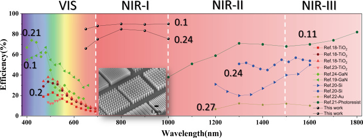
where r, ω, and F are the radial coordinates, angular frequency, and the focal length. To eliminate the chromatic aberration, both the phase and the group delay around the central frequency ωd must be properly controlled in the Taylor expansion of (1). The first term can be controlled by properly designing the resonant response, the Pancharatnam−Berry (PB) phase, or the propagation phase24–27. The latter can be manipulated with optimizing the waveguide mode by choosing suitable effective refractive index neff and thickness h26–28. Silicon that offers both high refractive index and mature nanofabrication technology, was shown to enable achromatic metalenses with efficiencies up to 50–60% in the spectral range from 1000 to 1800 nm (squares in Fig. 1)19. At shorter wavelengths above the band edge, the metasurfaces’ performance was, however, strongly limited by the material absorption. Titanium dioxide (TiO2) is another promising, technologically relevant and CMOS compatible material that can potentially overcome the absorption limitation of silicon17,18,29. However, current TiO2 metasurface fabrication techniques rely on the atomic layer deposition (ALD) method, which is relatively slow, and restricts the thickness and aspect ratio to the values below 600 nm and 15, respectively15,17. Lalanne et al.30 pioneered an etching technique for TiO2 nanostructures with a height up to 990 nm and the first perspective for imaging31. The aspect ratio is still limited to 8.8–10. As a result, the transmittance of nanopillar is usually sacrificed to fulfill the required group delay. For wavelengths above 630 nm, achromatic metalens’ focusing efficiency reduces rapidly to below 30% (dots in Fig. 1). While Ndao et al.32 reported an average efficiency of ~70%, they sacrificed the focusing ability of the demonstrated metalens and reduced the NA to 0.066. By combining recursive ray-tracing and simulated phase libraries, the hybrid achromatic metalens also shows its potential in achieving high focusing efficiency and broadband achromatism20. But the multi-photon process is not ready for shorter wavelength and the photoresist device faces the challenge from long-term durability. Therefore, metalens-based optical imaging in the biological transparency window (650–1000 nm) has so far been severely limited. Moreover, the efficiencies of the demonstrated achromatic metalenses are far below their monochromatic counterparts and cannot convincingly outperform the compound diffractive lens33–36. In this work, to address the above-mentioned challenges in metalens realization, we demonstrate high-efficiency, polarization-insensitive, and broadband achromatic metalens operating in the first biological imaging window.
Fig. 1. Efficiency chart of the demonstrated broadband achromatic metalenses.
The efficiencies of broadband achromatic metalenses with numerical apertures (NA) above 0.1 are plotted in different colors. The results of this work are also presented (black dots). The inset is the tilt SEM image of our TiO2 nanostructures with pillar height of 1500 nm.
Results
Working principle
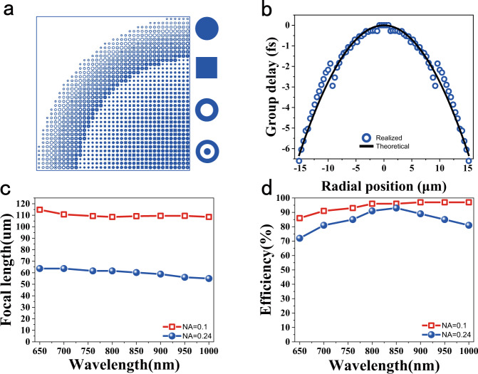
In our work, we control the metalens characteristics by carefully designing the group delay, since the material’s optical absorption is intrinsic and cannot be modified. The group delay range can be increased through simple geometry change, i.e., by making structures with larger aspect ratio/height. Here, we increase the pillar height to h = 1500 nm, which is 2.5 times larger compared to the previous reports. Similar to ref. 20, four types of nanopillars with circular-, ring-, square- and bipolar concentric ring-shaped cross-sections were employed as the metasurfaces building blocks (see Insets in Fig. 2a) to eliminate the polarization dependence. A parameter sweep of the nanopillar size and shape was done to build a library with the values of phase, group delay, and transmittance at the designed operational wavelength of 760 nm (see Supplementary Fig. 2). For an achromatic metalens with the diameter D = 30 µm and NA = 0.24, a particle swam optimization method was applied to optimize the nanostructures, minimizing the required group delay range and maximizing the smallest feature size37. Figure 2a shows the layout of a quarter of the developed metalens. It consists of four sets of TiO2 nanopillars with different cross-sections and a minimal feature size of 40 nm. The required group delay (black curves) of the achromatic metalens was matched to the propagating group delay in nanopillars (dots in Fig. 2b). As a result, broadband achromatic performance was expected. Figure 2c shows the numerically calculated focal lengths. The incident light with the wavelength 650 to 1000 nm, respectively, is focused by the TiO2 metalens to the designed position with a <7% variation, covering the first biological imaging window. The corresponding focusing efficiency is plotted as dots in Fig. 2d. The minimal and maximal focusing efficiencies are 72% at 650 nm and 93% at 850 nm, respectively. The averaged value in the entire operating spectrum is 83%. Note that the average efficiency can be up to 93% for the small NA of 0.1 and diameter of 25 µm (squares in Fig. 2d and details can be seen in Supplementary Fig. 3), surpassing all the current achromatic metalens demonstrations. In addition, as the nanopillars have at least fourfold rotational symmetry, the achromatic metalens is expected to be polarization insensitive, which is critical for biological applications38. Therefore, the developed TiO2 metalens with h = 1500 nm can potentially fill the so-called low-efficiency gap in available achromatic metalens designs.
Fig. 2. Design of the near-IR achromatic metalens.
a The layout of the quarter of the designed metalens. Four fundamental building blocks (unit cells) are enlarged in the insets. b The required group delay for broadband achromatism (solid line) and the values provided by the TiO2 nanostructures. c and d are the numerically calculated focal lengths and efficiencies of TiO2 metalenses with NA = 0.24 (dots) and NA = 0.1 (open squares) at different wavelengths. The diameters of two metalens are 30 and 25 µm, respectively.
Experiments
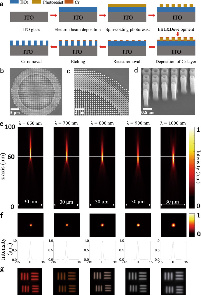
Experimental realization of TiO2 metalenses is a challenging task since the state of art pillar height is only 990 nm6,30. To overcome this challenge, we developed a top-down etching-based technology for fabricating TiO2 metalenses. First, 1500-nm-thick TiO2 membrane was deposited by the electron beam evaporation and coated with PMMA A2 resist, which was patterned with electron beam lithography. A lift-off process was applied to transfer the nanopatterns to Cr mask. Then, the membrane was etched with the reactive ion etching process (see details in Fig. 3a and “Methods”). After removing the Cr mask, the TiO2 nanostructures were created. Figure 3b, c depicts the top-view scanning electron microscope (SEM) images of the developed TiO2 metalens. It consists of 4725 nanopillars with four types of different cross-sections. Note that the nanopillars locations, shapes and feature sizes closely follow the numerical design. The tilt-view SEM images of TiO2 metalenses in Fig. 3d, the inset in Fig. 1, and the Supplementary Fig. 5 show that the nanopillars have nearly perfect vertical sidewalls with the measured tilt angle of sidewalls of around 89°−90°. Considering the smallest feature in the metalens, the achieved aspect ratio is around 37.5 or higher (Supplementary Fig. 5). The developed procedure for obtaining high-quality TiO2 nanostructures enabled the experimental realization of the metalens with the designed phase, group delay, and the corresponding high-efficiency broadband achromatism.
Fig. 3. The experimentally fabricated TiO2 metalens with NA = 0.24.
a The schematic of the fabrication process. A highly directional etching process was employed to fabricate TiO2 nanostructures. b and c are the top-view SEM images of achromatic metalens with different resolutions. Four types of nanostructures can be clearly identified. d The corresponding tilt-view SEM image of the metalens. e and f are the intensity profiles of focal spots in x-z plane and x-y planes at different wavelengths. The bottom panels depict the intensity distributions along the diameter (solid lines) and the fitted curves (dashed lines). g The images of element-6, group-7 of the 1951 Unites States Air Force resolution target recorded by the achromatic metalens.
The optical properties of the demonstrated TiO2 achromatic metalens were characterized using optical setup in Supplementary Fig. 6. The focal lengths at different wavelengths were obtained by measuring the cross-sectional intensity profiles along the propagation direction (Fig. 3e). In the broad wavelength range from 650 to 1000 nm, the incident light was focused to a bright spot ~60 µm away from the metalens with a small variation. The achieved values of both the focal length and the NA = 0.24 match the numerical design very well.
To demonstrate the realization of a broadband achromatic metalens for the first biological imaging window, Fig. 3f shows the light intensity profiles in the x-y plane at different wavelengths. The focal spot is a circular point at each wavelength. By fitting the intensity distributions along the diameter, all of the calculated Strehl ratios are larger than 0.81 and the full widths at half maximum (FWHM) deviate <9% from the theoretical values, clearly demonstrating that the focal spots are diffraction limited. The 1951 United State Air Force (USAF) resolution test chart was used as a target to test the imaging capability of the developed metalens. For the incident light with the wavelength of 650 nm, the metalens is able to resolve element-4 of group 8, giving a resolution above 1.38 µm. While the resolution limit is dependent on the wavelength, the image of element-6 of group 7 was clearly recorded at all wavelengths without tuning the metalens and the target (see Fig. 3g), confirming the broadband achromatism of our metalens very well.
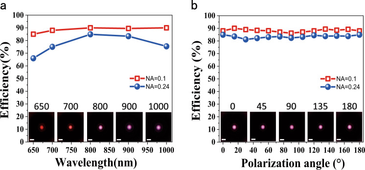
Compared with the achromatism, the focusing efficiency is a more critical criterion for filling the near-IR gap. Similar to refs. 2,8,9, we measured the efficiency by directly comparing the optical power of the focused light with the power of the incident light. The dots in Fig. 4a shows the experimentally recorded efficiencies of the TiO2 metalens with NA = 0.24. The lowest efficiency is ~65% at 650 nm, whereas the highest value is even ~85% at 800 nm. The averaged efficiency for the entire spectral range is ~77.1%, only a few percent lower than the numerical design. This is consistent with the high-quality fabrication of nanopillars since the efficiency reduces rapidly if the sidewall deviates from 90° in the vertical direction.
Fig. 4. Focusing efficiencies of the developed TiO2 metalenses.
a The experimentally recorded focusing efficiency of the TiO2 metalens with NA = 0.24 (dots) and NA = 0.1 (open squares) as the function of the incident wavelength. Here, the incident light is un-polarized. b The dependence of the focusing efficiencies at 800 nm on the polarization. The insets in (a) and (b) are images of the focal spots of the metalens with NA = 0.1 at different wavelengths and different polarization, respectively.
Compared with the previous reports, the observed averaged efficiency is record-high. More interesting, we find that the averaged focusing efficiency of the developed TiO2 metalens can be furthered improved at smaller NAs. When the NA is 0.1, the minimal and maximal focus efficiencies of the metalens at 650 nm and 700 nm are 85% and 90.2%, respectively (see open squares in Fig. 4a and details in Supplementary Fig. 3). The averaged efficiency from 650 to 1000 nm is as high as 88.5%. Since the Fresnel loss at the bottom and etched interfaces are not fully corrected, the averaged high-efficiency can reach above 90% that is superior to the commercial micro-lenses. According to the prediction in refs. 4,5, such high-efficiency broadband achromatic TiO2 metalens can become a game changer in practical applications of flat photonics.
Polarization insensitivity is another important characteristic for applications in the near-IR window. Figure 4b shows the focusing efficiencies of the demonstrated TiO2 metalenses at 800 nm at different polarization states. With the change of polarization, the efficiency of metalenses with NA = 0.24 and NA = 0.1 are almost flat at 85 and 89% for different linear polarization and circular polarization, consistent with the results of the non-polarized case in Fig. 4a. Similar polarization-insensitive characteristics hold true for all other wavelengths (see Supplementary Fig. 8).
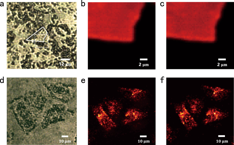
After we have demonstrated that the developed metalenses can successfully address the low-efficiency gap, we further explored the potential of TiO2 metalenses in upconversion imaging. In this experiment, the lanthanide-doped nanocrystals (NCs), which are widely used in bioimaging and labeling, were spread and aggregated on a glass substrate39. An additional layer of polystyrene (PS) spheres was deposited on top of the NC clusters. Under a conventional microscope, the NCs clusters were buried in PS spheres and cannot be identified (see Fig. 5a). Then, the continuous wave (CW) laser at 980 nm was focused by the TiO2 metalens onto the lanthanide-doped NCs clusters. The upconversion fluorescence centered at 655 nm with a linewidth of 20 nm was collected by the same metalens and recorded by a CCD camera (see Supplementary Fig. 9). By scanning the sample with a three-dimensional translation stage, the image can be reconstructed by combing the collected signals for each excitation point. The results are plotted in Fig. 5b. In contrast to conventional microscope image, the sharp edges of the NCs based microplate can be clearly seen in upconversion imaging. The resolution limit is around 1.46 µm, which is determined by the point spread function and the diffraction limit at the emission wavelength. For a direct comparison, the upconversion microscope image has been captured with a commercial achromatic objective lens with NA = 0.26 (Fig. 5c). Both the metalens and the objective lens can capture the structural information of microplate with two-photon excitation with no obvious difference in resolution and intensity distribution (see Supplementary Figs. 10 and 11).
Fig. 5. Upconversion imaging with the metalens.
a The microscope image of nanocrystals (NCs) on a microplate covered with polystyrene spheres under the white light illumination. The sample is marked with the dashed lines. b The upconversion fluorescent image recorded by the achromatic metalens with NA = 0.24. c The upconversion fluorescent image recorded by a commercial achromatic objective lens with N = 0.26 (MY10X-823, Mitutoyo). d The microscope image of HeLa cells with upconversion NCs. e and f and the upconversion fluorescent images recorded by the metalens and a commercial objective lens.
Potential application of the developed TiO2 achromatic metalens for biological imaging was also evaluated. For that, the HeLa cells containing lanthanide-doped NCs were prepared (Fig. 5d) and optically excited. Figure 5e depicts the fluorescent image of HeLa cells under two-photon excitation. Compared with the bright field microscope image in Fig. 5d, more detailed internal structures of the cell were captured. The image quality and the resolution were close to the ones recorded by the commercial objective lens with the similar NA (Fig. 5f). Thus, the demonstrated achromatic TiO2 metalens can perform on par with the commercial products for optical imaging. Considering its compactness, flatform, high-efficiency, polarization insensitivity, and diffraction-limit resolution, the proposed achromatic TiO2 metalenses could trigger a revolution in on-board biomedical diagnosis.
Discussion
In summary, we developed a top-down fabrication technique for the realization of superior quality, record-high aspect ratio TiO2 metasurfaces. With the increase in the metalens’ thickness, the group delay range provided by the TiO2 nanopillars was dramatically enhanced. As a result, high-efficiency, broadband achromatic metalenses were designed and demonstrated in the near-IR biological window for an unpolarized incident light. The focusing efficiencies of the demonstrated achromatic metalenses were as high as 77.1% and 88.5% for the NA of 0.24 and 0.1, respectively, while the maximal focusing efficiency was above 90%. The proposed achromatic metalenses with record-high efficiencies and mass-manufacturable fabrication process could be extended to the visible spectrum as well (see Supplementary Fig. 12) and can potentially trigger a revolution in applications of flat optoelectronics17,40–43. Our work is also expected to accelerate the commercialization and biological applications of metasurfaces in portable devices as well as untethered microrobots.
Methods
Numerical simulation
The elements of phase-dispersion library were simulated by a finite element method-based commercial software COMSOL Multiphysics. Each element was simulated under linearly polarized illumination, and the propagation direction of light is along z-axis. The material properties of TiO2 and ITO-coated glass are all considered. Periodic boundary conditions were applied to the x- and y-directions and perfectly matched layer boundary conditions were applied to the z-directions. For each simulation under sweep parameter with respect to the wavelength from 650 to 1000 nm, then the phase spectrum was obtained. We linearly fit the phase spectrum of each element to obtain the group delay. To improve the achromatic performance, the achromatic metalens elements should have good linearity, then any element has an R-squared value <0.995 was dropped. In order to demonstrate the achromatic metalens focusing performance, the metalens was modeled in finite-domain time-difference simulations (Lumerical FDTD Solutions). Perfectly matched layer boundary conditions were used along the transverse and longitudinal directions and under plane wave illumination.
Deposition of TiO2 film
The TiO2 film was deposited by electron beam evaporation. The ITO-coated glass substrate is cleaned and placed into the modified electron beam evaporator (Syskey, 30 kV acceleration voltage). The vacuum pressure is pumped to 2 × 10⁻⁷ Torr and the deposition rate is fixed at 0.6 Å/s. The TiO2 film with 1500 nm thickness is achieved after 6.94 h continuous deposition.
Fabrication of metalens
The metalens was fabricated using electron-beam lithography (EBL) on 1500 nm thick titanium dioxide film with quartz substrate to pattern the specific arrays. Firstly, PMMA A2 e-beam resist layer is deposited by spin-coating on titanium dioxide film. Then the sample is exposed through EBL and the patterns are revealed after the development process in MIBK/IPA. Subsequently, 30 nm thick Cr layer as hard mask deposited on sample used electron-gun evaporator and lift-off process is done in solution of PG remover. Next, the patterns are transferred to titanium dioxide film by reactive ion etching (RIE) in Oxford 800 Plus. SF6, CHF3 and O2 are utilized in the etching process. The RF power is 100 W and the pressure is 9 mTorr. The ratio of CHF3/SF6 is tuned to 5.5, effectively improving the anisotropy of etching. O2 is added to accelerate the etching speed in the vertical direction. The final sample can be obtained after removal of the Cr hard etching mask.
The optical characterization of metalens
The metalenses were characterized using a home-built microscope as shown in Supplementary Fig. 6. A collimated laser beam was converted into linearly polarized light after passing through the linear polarizer, Light exiting the polarizer is passing through the objective lens and incident on the metalens, then passes through another objective lens, and finally focuses on the CCD through a tube lens. The longitudinal intensity distribution of the metalens is acquired through a stack of 2D images by changing metalens position in predefined increments. The light intensity distribution of different wavelengths is obtained by inserting color filters.
For focusing efficiency measurement of the metalens, we measured the power in the focal spot (the power of transmission light passing through a circular area with radius of 3*FWHM) and divided by the incident light power (the power of incident light passing through a circular area with radius same as metalens). Note that the efficiency can be further improved by fully correct the Fresnel loss the etched interface and the bottom interface.
Supplementary information
Acknowledgements
This research was supported by the National Key Research and Development Project (Grant No. 2018YFB2200403), National Natural Science Foundation of China (Grant Nos. 12025402, 11974092, and 11934012), Shenzhen Fundamental research projects (Grant No. JCYJ20180507184613841, JCYJ20180507183532343, JCYJ20200109112805990, and JCYJ20200109113003946), Shenzhen engineering laboratory on organic-inorganic perovskite devices, and the Fundamental Research Funds for the Central Universities(Grant No. HIT. BRET. 2021009). Purdue authors acknowledge support from the Air Force Office of Scientific Research (AFOSR) grant FA9550-18-1-0002 and FA9550-20-1-0124.
Author contributions
S.X. designed and supervised the experiment. Y.W. and W.Y. fabricated the samples. Q.C. designed the achromatic metalens. Z.J. and Y.W. performed the optical characterization. L.J. and X.M. provided the upconversion nanoparticles and HeLa cells. Q.S., A.B., J.H., V.S. and S.X. discussed the results and prepared the manuscript.
Data availability
All the data supporting the findings of this study are available within the article, its Supplementary Information files, or accessed under the link https://pan.baidu.com/s/4lag6i6F.
Competing interests
The authors declare no competing interests.
Footnotes
Peer review informationNature Communications thanks the anonymous reviewer(s) for their contribution to the peer review of this work. Peer reviewer reports are available.
Publisher’s note Springer Nature remains neutral with regard to jurisdictional claims in published maps and institutional affiliations.
These authors contributed equally: Yujie Wang, Qinmiao Chen, Wenhong Yang, Ziheng Ji.
Supplementary information
The online version contains supplementary material available at 10.1038/s41467-021-25797-9.
References
- 1.Pahlevaninezhad H, et al. Nat. Photon. 2018;12:540–547. doi: 10.1038/s41566-018-0224-2. [DOI] [PMC free article] [PubMed] [Google Scholar]
- 2.Fang N, Lee H, Sun C, Zhang X. Sub-diffraction-limited optical imaging with a silver superlens. Science. 2005;308:534–537. doi: 10.1126/science.1108759. [DOI] [PubMed] [Google Scholar]
- 3.Gissibl T, Thiele S, Herkommer A, Giessen H. Two-photon direct laser writing of ultracompact multi-lens objectives. Nat. Photon. 2017;10:554–560. doi: 10.1038/nphoton.2016.121. [DOI] [Google Scholar]
- 4.Khorasaninejad M, Capasso F. Metalenses: versatile multifunctional photonic components. Science. 2017;358:eaam8100. doi: 10.1126/science.aam8100. [DOI] [PubMed] [Google Scholar]
- 5.Chen WT, Zhu AY, Capasso F. Flat optics with dispersion-engineered metasurface. Nat. Rev. Mater. 2020;5:604–620. doi: 10.1038/s41578-020-0203-3. [DOI] [Google Scholar]
- 6.Lalanne P, Chavel P. Metalenses at visible wavelengths: past, present, perspectives. Laser Photon. Rev. 2017;11:1600295. doi: 10.1002/lpor.201600295. [DOI] [Google Scholar]
- 7.Kock WE. Metallic delay lenses. Bell Syst. Tech. 1948;34:321–339. [Google Scholar]
- 8.Stork W, Streibl N, Haidner H, Kipfer P. Artificial distributed-index media fabricated by zero-order gratings. Opt. Lett. 1991;16:1921–1923. doi: 10.1364/OL.16.001921. [DOI] [PubMed] [Google Scholar]
- 9.Ishii S, Kildishev AV, Shalaev VM, Chen K-P, Drachev VP. Metal nanoslit lenses with polarization-selective design. Opt. Lett. 2011;36:451–453. doi: 10.1364/OL.36.000451. [DOI] [PubMed] [Google Scholar]
- 10.Yu N, et al. Light propagation with phase discontinuities: generalized laws of reflection and refraction. Science. 2011;334:333–337. doi: 10.1126/science.1210713. [DOI] [PubMed] [Google Scholar]
- 11.Ni X, Emani NK, Kildishev AV, Boltasseva A, Shalaev VM. Broadband light bending with plasmonic nanoantennas. Science. 2012;335:427. doi: 10.1126/science.1214686. [DOI] [PubMed] [Google Scholar]
- 12.Lin D, Fan P, Hasman E, Brongersma ML. Dielectric gradient metasurface optical elements. Science. 2014;345:298–302. doi: 10.1126/science.1253213. [DOI] [PubMed] [Google Scholar]
- 13.Arbabi A, Horie Y, Ball AJ, Bagheri M, Faraon A. Subwavelength-thick lenses with high numerical apertures and large efficiency based on high-contrast transmit arrays. Nat. Commun. 2015;6:7069. doi: 10.1038/ncomms8069. [DOI] [PubMed] [Google Scholar]
- 14.Yu YF, et al. High transmission dielectric metasurface with 2π phase control at visible wavelengths. Laser Photon. Rev. 2015;9:412–418. doi: 10.1002/lpor.201500041. [DOI] [Google Scholar]
- 15.Khorasaninejad M, et al. Metalenses at visible wavelengths: diffraction-limited focusing and subwavelength resolution imaging. Science. 2016;352:1190–1194. doi: 10.1126/science.aaf6644. [DOI] [PubMed] [Google Scholar]
- 16.Liang H, et al. Ultrahigh numerical aperture metalens at visible wavelengths. Nano Lett. 2018;18:4460–4466. doi: 10.1021/acs.nanolett.8b01570. [DOI] [PubMed] [Google Scholar]
- 17.Chen W-T, et al. A broadband achromatic metalens for focusing and imaging in the visible. Nat. Nanotechnol. 2018;13:220–226. doi: 10.1038/s41565-017-0034-6. [DOI] [PubMed] [Google Scholar]
- 18.Wang S, et al. A broadband achromatic metalens in the visible. Nat. Nanotechnol. 2018;13:227–232. doi: 10.1038/s41565-017-0052-4. [DOI] [PubMed] [Google Scholar]
- 19.Shrestha S, Overvig AC, Lu M, Stein A, Yu N. Broadband achromatic dielectric metalenses. Light Sci. Appl. 2018;7:85. doi: 10.1038/s41377-018-0078-x. [DOI] [PMC free article] [PubMed] [Google Scholar]
- 20.Balli F, Sultan M, Lami SK, Hastings JT. A hybrid achromatic metalens. Nat. Commun. 2020;11:3892. doi: 10.1038/s41467-020-17646-y. [DOI] [PMC free article] [PubMed] [Google Scholar]
- 21.Wang S, et al. Broadband achromatic optical metasurface devices. Nat. Commun. 2017;8:187. doi: 10.1038/s41467-017-00166-7. [DOI] [PMC free article] [PubMed] [Google Scholar]
- 22.Khorasaninejad M, et al. Achromatic metalens over 60 nm bandwidth in the visible and metalens with reverse chromatic dispersion. Nano Lett. 2017;17:1819–1824. doi: 10.1021/acs.nanolett.6b05137. [DOI] [PubMed] [Google Scholar]
- 23.Lin RJ, et al. Achromatic metalens array for full-colour light-field imaging. Nat. Nanotechnol. 2019;14:227–231. doi: 10.1038/s41565-018-0347-0. [DOI] [PubMed] [Google Scholar]
- 24.Bomzon Z, Biener G, Kleiner V, Hasman E. Space-variant Pancharatnam–Berry phase optical elements with computer-generated subwavelength gratings. Opt. Lett. 2002;27:1141–1143. doi: 10.1364/OL.27.001141. [DOI] [PubMed] [Google Scholar]
- 25.Kuznetsov AI, Miroshnichenko AE, Brongersma ML, Kivshar YS, Luk’yanchuk B. Optically resonant dielectric nanostructures. Science. 2016;354:aag2472. doi: 10.1126/science.aag2472. [DOI] [PubMed] [Google Scholar]
- 26.Sauvan C, Lalanne P, Lee MSL. Broadband blazing with artificial dielectrics. Opt. Lett. 2004;29:1593–1595. doi: 10.1364/OL.29.001593. [DOI] [PubMed] [Google Scholar]
- 27.Ribot C, et al. Broadband and efficient diffraction. Adv. Opt. Mat. 2013;1:489–493. doi: 10.1002/adom.201300215. [DOI] [Google Scholar]
- 28.Gigli, C. et al. Fundamental limitations of Huygens metasurfaces for optical beam shaping. Laser Photon. Rev.15, 2000448 (2021).
- 29.Yoon G, Kim K, Huh D, Lee H, Rho J. Single-step manufacturing of hierarchical dielectric metalens in the visible. Nat. Commun. 2020;11:2268. doi: 10.1038/s41467-020-16136-5. [DOI] [PMC free article] [PubMed] [Google Scholar]
- 30.Lalanne P, Astilean S, Chavel P, Cambril E, Launois H. Design and fabrication of blazed binary diffractive elements with sampling periods smaller than the structural cutoff. J. Opt. Soc. Am. A. 1999;16:1143–1156. doi: 10.1364/JOSAA.16.001143. [DOI] [Google Scholar]
- 31.Lee MSL, et al. Imaging with blazed-binary diffractive elements. J. Opt. A. 2002;4:s119–s124. doi: 10.1088/1464-4258/4/5/358. [DOI] [Google Scholar]
- 32.Ndao A, et al. Octave bandwidth photonic fishnet-achromatic-metalens. Nat. Commun. 2020;11:3205. doi: 10.1038/s41467-020-17015-9. [DOI] [PMC free article] [PubMed] [Google Scholar]
- 33.Banerji S, et al. Imaging with flat optics: metalenses or diffractive lenses? Optica. 2019;6:805–810. doi: 10.1364/OPTICA.6.000805. [DOI] [Google Scholar]
- 34.Engelberg J, Levy U. The advantages of metalenses over diffractive lenses. Nat. Commun. 2020;11:1991. doi: 10.1038/s41467-020-15972-9. [DOI] [PMC free article] [PubMed] [Google Scholar]
- 35.Mohammad N, Meem M, Shen B, Wang P, Menon R. Broadband imaging with one planar diffractive lens. Sci. Rep. 2018;8:2799. doi: 10.1038/s41598-018-21169-4. [DOI] [PMC free article] [PubMed] [Google Scholar]
- 36.Wang P, Mohammad N, Menon R. Chromatic-aberration-corrected diffractive lenses for ultra-broadband focusing. Sci. Rep. 2016;6:21545. doi: 10.1038/srep21545. [DOI] [PMC free article] [PubMed] [Google Scholar]
- 37.Chen WT, Zhu AY, Sisler J, Bharwani Z, Capasso F. A broadband achromatic polarization-insensitive metalens consisting of anisotropic nanostructures. Nat. Commun. 2019;10:355. doi: 10.1038/s41467-019-08305-y. [DOI] [PMC free article] [PubMed] [Google Scholar]
- 38.Arbabi E, et al. Two-photon microscopy with a double wavelength metasurface objective lens. Nano Lett. 2018;18:4943–4948. doi: 10.1021/acs.nanolett.8b01737. [DOI] [PubMed] [Google Scholar]
- 39.Zhu H, et al. Amplified spontaneous emission and lasing from Lanthanide-doped uo-conversion nanocrystals. ACS Nano. 2013;7:11420–11426. doi: 10.1021/nn405387t. [DOI] [PubMed] [Google Scholar]
- 40.Park J-S, et al. All-glass, large metalens at visible wavelength using deep-ultraviolet projection lithography. Nano Lett. 2020;19:8673–8682. doi: 10.1021/acs.nanolett.9b03333. [DOI] [PubMed] [Google Scholar]
- 41.Kwon H, Arbabi E, Kamali SM, Faraji-Dana M, Faraon A. Single-shot quantitative phase gradient microscopy using a system of multifunctional metasurfaces. Nat. Photon. 2020;14:109. doi: 10.1038/s41566-019-0536-x. [DOI] [Google Scholar]
- 42.Schlickriede C, et al. Nonlinear imaging with all-dielectric metasurfaces. Nano Lett. 2020;20:4370–4376. doi: 10.1021/acs.nanolett.0c01105. [DOI] [PubMed] [Google Scholar]
- 43.Rogers ETF, et al. Far-field unlabeled super-resolution imaging with superoscillatory illumination. APL Photon. 2020;5:066107. doi: 10.1063/1.5144918. [DOI] [Google Scholar]
Associated Data
This section collects any data citations, data availability statements, or supplementary materials included in this article.
Supplementary Materials
Data Availability Statement
All the data supporting the findings of this study are available within the article, its Supplementary Information files, or accessed under the link https://pan.baidu.com/s/4lag6i6F.


