

Abstract
The high electronegativity between the atoms of two-dimensional (2D) group-III nitrides makes them attractive to demonstrating a strong out-of-plane piezo-electricity effect. Energy harvesting devices can be predicted by cultivating such salient piezoelectric features. This work explores the tribo-piezoelectric properties of 2D-indium nitride (InN) as a promising candidate in nanogenerator applications by means of first-principles calculations. In-plane interlayer sliding between two InN monolayers leads to a noticeable rise of vertical piezoelectricity. The vertical resistance between the InN bilayer renders tribological energy by the sliding effect. During the vertical sliding, a shear strength of 6.6–9.7 GPa is observed between the monolayers. The structure can be used as a tribo-piezoelectric transducer to extract force and stress from the generated out-of-plane tribo-piezoelectric energy. The A–A stacking of the bilayer InN elucidates the highest out-of-plane piezoelectricity. Any decrease in the interlayer distance between the monolayers improves the out-of-plane polarization and thus, increases the inductive voltage generation. Vertical compression of bilayer InN produces an inductive voltage in the range of 0.146–0.196 V. Utilizing such a phenomenon, an InN-based bilayer compression-sliding nanogenerator is proposed, which can tune the generated tribo-piezoelectric energy by compressing the interlayer distance between the InN monolayers. The considered model can render a maximum output power density of ~ 73 mWcm−2 upon vertical sliding.
Subject terms: Energy science and technology, Materials science, Nanoscience and technology
Introduction
In recent years, nanogenerator and nanoscale energy harvesting devices are attracting tremendous attention due to their promising applications in low-power electronics and self-powered sensors1–9. In a nanogenerator, electrical energy can be attained from mechanical or thermal energy by small-scale physical changes. Two lucrative ways to form a nanogenerator are the consideration of the piezoelectric8,10–12 and triboelectric8,13–16 effects. When mechanical deformation is enforced on semiconductor materials, polarized charge is generated via the piezoelectric effect. In this context, vertical in-plane piezoelectricity in Janus transition metal dichalcogenides (TMDs)15,17 materials has been observed. Such a piezoelectricity phenomenon can be used to formulate new nanogenerators. Piezoelectrical nanogenerators have also been formulated utilizing interfacial ZnO nanostructures11, a lateral ZnO nanowire array13, and lead zirconate titanate nanofibers (PZT)9. In the case of the triboelectric effect, with the variation in the mechanical contact or friction between two layers of nanomaterials, temporary static charges are generated. Two triboelectrically charged surfaces can be considered to form a triboelectric nanogenerator18–20 utilizing in-plane sliding21–23 or vertical movement24,25 between them. The formulation of nanogenerator often involves both piezoelectric polarization and triboelectric charges. The tribo-piezoelectric phenomenon is demonstrated by Karumuthil et al., where they have taken the poly dimethyl siloxane-based hybrid nanocomposite8 and have reported enhanced current characteristics with improved mechanical to electrical energy conversion efficiency. Energy conversion efficacy can also be improved by incorporating an additional layer21 of nanomaterial between the electrodes and their substrates in a nanogenerator. New nanomaterials and structural patterns are considered to identify versatile and efficient tribo-piezo nanogenerators.
To develop nanoscale energy harvesting devices, two-dimensional (2D) materials26–30 are fascinating and promising due to their extraordinary features such as high electron mobility, large quantum spin hall effects, high carrier mobility, and very low thickness. In particular, transition metal dichalcogenides31 and Janus monolayer material WS-X (X = Se and Te)32 can demonstrate vertical and in-plane piezoelectrical properties. Among other 2D materials, group-III nitrides are prominent due to their diverse applications in the field of nanoelectronics, optoelectronics, spintronics, and heterojunction devices fabrications28,29,33,34. Since the group-III nitrides are electronegative in nature, it is predicted that these materials will demonstrate significant polarization with external mechanical disposition35–40. To this extent, Nan et al.41 have investigated piezoelectricity in 2D hexagonal boron nitride nanosheets (BNNS) and posited that piezoelectricity in BNNS strongly depends on the microscopic shape of the structure. In a single layer InN nanowire nanogenerator, a piezoelectric potential as high as 1 V can be obtained, and the polarity of the potential depends on the direction of the applied transverse force42. Guo et al.43 have demonstrated that the surface hydrogenated 2D group-III nitrides (AlN, GaN, InN) show both in-plane and out-of-plane piezoelectrical properties with external strain. Nevertheless, a detailed understanding of the contribution of both the triboelectric and piezoelectrical effects in the formation of nanogenerators of 2D group-III nitrides is still scarce.
Among the group-III nitrides, 2D-InN is lucrative due to its graphene-like hexagonal structure, strong quantum confinement, and stronger in-plane and out-of-plane excitonic effects with binding energies substantially greater than the room temperature thermal energy44–47. Moreover, InN can demonstrate optoelectrical properties around the visible to infrared spectral ranges46 and retains a 2D electron gas in the quantum well, a property well cherished for making high electron mobility transistors48. The large deviation between the electronegativity of In (1.78) and N (3.04) atoms predicts InN to display strong polarization in the milieu of in-plane external mechanical force and strain. However, to apply this material to nanogenerator applications, a detailed investigation of mechanical deformation and friction to generate electrical potential is an essential prerequisite.
In this work, the tribo-piezoelectricity effect of bilayer InN is explored through first-principles density functional theory investigations. At two separate interlayer distance points, a mutual transverse sliding effect is incorporated. It is observed that transverse sliding along a special direction can engender vertical polarization. Strong out-of-plane piezoelectricity can be achieved and tuned by changing the interlayer distance between the bilayer. With a decrease in the interlayer distance, the out-of-plane piezoelectric charge polarization increases and thus, renders the in-plane sliding energy barrier higher. The effect of the sliding variation results in charge transfer and charge redistribution between the layers. Moreover, the shear strength, the polarization deviation, and the energy variation with change in the interlayer distance demonstrate tunable tribo-piezoelectric properties. Since a deviation in the interlayer displacement can engender out-of-plane piezoelectricity, a compressive-sliding nanogenerator17 with an InN bilayer structure is proposed based on the tribo-piezoelectric effect and can render an electrical potential as high as ~ 0.2 V.
Methods
A bilayer of InN is initially considered to investigate the mechanical deformation and friction. The rhombus unit cell of bilayer InN consists of 2-In and 2-N atoms. After structural optimization and relaxation, the bottom InN monolayer is kept fixed, and transverse sliding is incorporated into the top InN layer. As a result, the structure translates to different places in the XY-plane. The relaxation process is carried out for each position, and a constant interlayer spacing is maintained between N atoms in the top and bottom layers. During the in-plane sliding around the x–y axis of the top layer at an interlayer distance, the potential energy surface (PES) is calculated by:
| 1 |
where represents the PES at the (x, y) coordinate. refers to the energy obtained at the (x, y) coordinate and is the lowest energy of the system. The relative vertical polarization at a specific (x, y) coordinate can be quantified by considering the induced dipole moment as:
| 2 |
With D being the vertical dipole moment and A is the area of the unit cell. In the initial equilibrium state, because of the higher electronegativity of the N atoms, the charge shifts to the N atoms of the InN monolayers and causes out-of-plane electric charge polarization. Thus, the initial vertical polarization () of the InN bilayer can be set at 0. The polarization deviation surface (PDS) with in-plane sliding can then be calculated from the magnitude of vertical polarization by:
| 3 |
Here and ) are the PDS and the vertical polarization at the (x, y) coordinate. When the sliding friction between the layers is incorporated, a higher vertical polarization is predicted. The amount of shear strength relative to the sliding of the layer can be obtained from the relation:
 |
4 |
Here  is the attained shear strength from the maximum amount of static resistance (), which acts on the InN monolayer within area , during the sliding process.
All the calculations in this work are performed using density functional theory (DFT) employing the plane wave self-consistent field (PWscf) package of Quantum Espresso49,50. The Perdew-Burke-Ernzerhof (PBE)51 functional for the generalized gradient approximation (GGA) is used to describe the exchange–correlation functional. In the PWscf code, Kresse-Joubert projector augmented wave (KJPAW)52 potentials are used to describe the electron–ion interactions. The optB86b-vdW53,54 functional is employed to represent the Van-der Waals (vdW) weak intermolecular interaction. To ensure accurate simulation for the energies and interatomic distances at the equilibrium, the original PBE vdW-DF is modified by optB86b-vdW interaction53–55. The Brillouin zone integration is performed using a 2D-centered Monkhrost-Pack56 k-mesh grid of 15 × 15 × 1. For accurate convergence of the ground state electron density, an energy cut-off value of 10−8 a. u. is used. The kinetic energy cut-offs for the wave function and charge densities are set at 50 Ry and 400 Ry, respectively. Moreover, a force convergence threshold of 10−3 eV/nm is used for accurate stress and force calculations. A 15 Å vacuum region is used to ensure no direct interaction between the monolayers and bilayers.
Results and discussion
The investigation starts with the structural optimization of the InN monolayer. After relaxation, the obtained lattice constant is 3.58 Å with a zero buckling height. Our result complies well with the result of Sahin et al.57, where they obtained a lattice constant for InN of 3.57 Å with the local density approximation (LDA). Two energetically stable structures, A–B and A–C, are found for bilayer InN, which corresponds well with earlier study46. In the A–B stacking pattern, the N and In atoms are placed over the In atom and the center of the hexagon in the bottom layer, whereas, in the A–C stacking, the In and N atoms of the top layer are placed at the N atom and the center of the hexagon in the bottom layer, respectively, as shown in Fig. 1. The InN monolayers are separated by an interlayer distance measured between the top and bottom N atoms. The stable interlayer distance for the A–B and A–C patterns are found as 2.81 Å and 2.80 Å, respectively, by the calculation of the binding energy with respect to interlayer distance. Since the minimum binding energy point corresponds to the (local) equilibrium geometry, it will result in stable electronic properties58–61. Besides, the calculation of the binding energy of a material structure provides significant information about the stability of the material. A negative binding energy is obtained by a stable interlayer distance, with a higher negative value implying more stability than a smaller value. For the InN bilayer structure, we obtained negative (stable) binding energies when the interlayer distance was in the range of 2.41 to 2.81 Å. This range of interlayer distance is then considered as a criterion for selecting the range for the stable interlayer distance to employ vertical compressive sliding of the top InN layer to attain higher maximum energy corrugation.
Figure 1.

Top view of the (a) A–A, (b) A–B, and (c) A–C stacking patterns. (d) Side view of the bilayer showing the interlayer distance ‘d’ between the monolayers. Here, the blue and cyan colors refer to N and In atoms, respectively. a1 and a2 denote the in-plane lattice constants.
The effect of transverse sliding is investigated at the two different interlayer distances (2.81 Å and 2.51 Å). The potential energy surface (PES) and polarization deviation surface (PDS) at various sliding locations are calculated and depicted in Fig. 2. The PES and PDS plots are periodically repeating in nature, which commensurates with the equilibrium geometry of the flat honeycomb structured group-III 2D nitrides37. According to Fig. 2, whenever the initial pattern slides to the resemblance of the A–A stacking pattern, very high vertical polarization is demonstrated. Moreover, such high vertical polarization increases for a low interlayer distance. On the other hand, the A–B stacking pattern renders very low vertical polarization with a change in the interlayer distance. Moreover, the A–B stacking has a substantially weaker response to interlayer distance than the A–C stacking. Thus, the A–A stacking pattern will attain the maximum polarization enhancement, and the A–B stacking pattern is taken as the initial state. Nonetheless, without external mechanical stimulus or restraint, the A–A stacking is not energetically favorable. During the in-plane sliding of the A–B pattern, only a lateral driving force that is higher than the interlayer shear strength and resistive force can trigger a transition to the A–A pattern. Interlayer sliding and accompanying resistance are tribological phenomena, whereas shifting to A–A stacking with a fixed interlayer distance enhances vertical polarization significantly. As a result, the out-of-plane polarization amplification caused by in-plane interlayer sliding in the InN bilayer can be regarded as a tribo-piezoelectric phenomenon. The piezoelectricity is the result of tribological energy conversion, which overcomes the energy barrier of sliding resistance. To drive the InN bilayer to the A–A state, which can be seen of as the conversion of tribological energy to electricity, external driving force and pressure are required.
Figure 2.

The potential energy surface (PES) (on-left) and polarization deviation surface (PDS) (on-right) for in-plane sliding of the InN bilayer when the interlayer distance is (a) 2.81 Å and (b) 2.51 Å.
At a fixed interlayer distance, the process of overcoming the energy barrier related to resistive force and interlayer shear strength maintains the triboelectric effect. As such, the vertical plane sliding that generated out-of-plane vertical polarization will be the result of the tribo-piezoelectric effect. Unlike previous studies8,11, where the triboelectric effect renders static charges, in our study, the tribological energy engenders piezoelectricity. Similar tribo-piezoelectric behavior has been observed in the Janus transition metal dichalcogenide bilayers by Cai et al.17. The energy corrugation (∆E) in the PES of the InN bilayer thus is a function of vertical interlayer resistive frictions; a higher interlayer resistance and friction will generate a larger energy corrugation36.
The amount of tribo-piezoelectricity generation depends on the energy corrugation (∆E). Figure 3a represents the maximum polarization deviation (∆Pmax) with maximum energy corrugation (∆Emax) with the compressive variation of the interlayer distance from 2.81 Å to 2.41 Å. According to Fig. 3a, the maximum polarization deviation increases linearly with an increase in the maximum energy corrugation. The higher the energy required to overcome the interlayer sliding friction, the larger value of vertical polarization will be achieved. The maximum static resistance force acting on the sliding process can be utilized to calculate the relative shear strength from Eq. (4). Figure 3b is a depiction of the shear strength related to an interlayer distance within the range of 2.41 Å to 2.81 Å. The maximum energy barrier deviation (754–1227 meV) and shear strength (6.6–9.7 GPa) during the vertical compressive sliding of the InN layer are higher than those obtained with the Janus transition metal dichalcogenide (TMD) bilayers ((180–480 meV) and (2.5–7.2 GPa), respectively17. A higher vertical polarization value (4.5–11.4 pC/m) can also be obtained with the InN bilayer than the Janus TMD bilayers (0.6–2.3 pC/m)17. A reduction in the interlayer distance renders a quadratic increase in both shear strength and maximum corrugated energy values. Thus, vertical compressive sliding is an efficient way to obtain higher triboelectric to electrical energy conversion. However, a structural change has been noticed in this process due to the effect of in-plane strain caused by vertical stress. The change in interlayer distance alters the interaction among the atoms of the bilayer; influence becomes stronger when the bilayer is placed at a lower interlayer spacing than the optimized value. When the interlayer distance was at its optimized point (2.81 Å), the lattice constant was 3.587 Å. But decreasing the interlayer distance results in a reduction of lattice constant. At a spacing of 2.51 Å and 2.41 Å, the lattice constant reduces to 3.553 Å and 3.549 Å, respectively. The system is relaxed for each time upon application of vertical stress, and the changes in the lattice constant are taken into consideration in the calculations.
Figure 3.
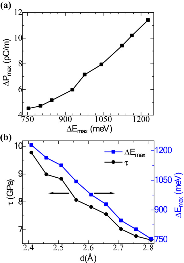
(a) The maximum polarization changes (pC/m) with the maximum sliding energy barriers (meV). (b) The variation of the interlayer shear strength (black line with filled circles) and maximum sliding energy barriers (blue line with blocks) with change in the interlayer distance of the InN bilayer.
To demonstrate the charge contribution to the observed tribo-piezoelectric property in the InN bilayer, the charge density difference (CDD) is investigated. Figure 4 represents the CDD between the InN monolayers at two interlayer distances (2.81 Å and 2.51 Å). The CDD is enumerated as , where is the total charge density of the InN bilayer, and refers to the charge density associated with the top and bottom InN layers. It can be seen that, for both interlayer displacements, the charge accumulates near the N-atoms of the monolayers and at the surface between them. Moreover, when the A–B (Fig. 4a,b) stacking pattern slides into the A–A (Fig. 4c,d) stacking pattern, the magnitude of the charge accumulation around the N-atoms drastically increases. For the A–A stacking pattern, with a lower interlayer distance (2.51 Å), the CDD can be improved significantly from that obtained at an interlayer distance of 2.81 Å. A large amount of charge accumulation around the N-atoms demonstrates higher out-of-plane polarization of the A–A stacking pattern.
Figure 4.

The charge density differences between the InN monolayers at 0.001 e/Å3. Here the upper two plots (a, b) refer to the A–B stacking pattern at an interlayer distance of 2.81 Å and 2.51 Å, respectively, and the lower two plots (c, d) refer to the A–A stacking pattern at an interlayer distance of 2.81 Å and 2.51 Å, respectively. Here, the red color refers to the charge accumulation, and the green color refers to the charge depletion.
With the variation of the interlayer distance, the average charge density differences for the top and bottom monolayers of InN are also observed. For this process, initially, zero normal force (Fn = 0) is applied in the Z-direction. The charge density differences within the monolayers can be defined as:
| 5 |
| 6 |
where and are the CDD at the top and bottom InN monolayers, and are the average charge densities of the N-atoms at the Z-direction with the interlayer variation, and and with zero normal forces. Figure 5a,b represent the average charge density variations with interlayer distances in the range of 2.81–2.41 Å. It can be seen that a lower interlayer separation causes a higher average charge density within the layers. For the A–B stacking pattern, with compression of the vertical displacement between the layers, a higher amount of charge density is observed at the top layer than the bottom layer. At the same time, the charge density of the top layer dominates in the A–A stacking pattern. The charge distribution between the top and bottom monolayers of InN complies well with the CDD plot (Fig. 4). The charge redistribution between the layers and atoms can be considered for developing a compressive-sliding nanogenerator. Since the majority of the charge accumulates near the N-atoms, the electron density around the N-surface will be higher than the interface electron density between the layers. Attaching electrodes at the top and bottom surfaces can engender a small voltage, as shown in Fig. 5c. For the A–A stacking pattern, a higher accumulation of inductive charges appears near the interface, as shown in Fig. 5d. Thus, a larger voltage can be extracted by forming a nanogenerator with the A–A stacking pattern. Additionally, the charge gain at the top and bottom layers with the vertical sliding process is shown in Fig. 5e. The charge gain is calculated by subtracting the monolayer charges between the unit cell of the A–A and A–B stacking patterns.
Figure 5.

(a, b) Average charge density differences at 0.001 e/Å3 on the two monolayers of the InN bilayer for (a) A–B stacking and (b) A–A stacking with the change in the interlayer distance. Relative inductive charge and voltage that are accumulated at the electrodes that contact with the surface of the top and bottom layers of the (c) A–B stacking and (d) A–A stacking. (e) Charge gain during the sliding of the top and bottom layer of the InN bilayer.
Next, considering the A–A stacking pattern, the maximum generated voltage is enumerated by considering the electrostatic potential differences (∆U) between the N-atoms of the top and bottom layers. The change in the electrostatic potential differences with interlayer variation is found at the monolayer surfaces by:
| 7 |
where
| 8 |
| 9 |
where and are the electrostatic potential variation at the top and bottom InN monolayers, and are the electrostatic potentials around the N-atoms at the top and bottom surfaces of the monolayers and and are the corresponding cases at zero normal forces. According to Fig. 6, a decrease in the interlayer distance causes a higher vertical polarization and renders a higher electrostatic potential at the top and bottom layers. Throughout the process, an induced voltage ranging from 0.146 to 0.196 V can be obtained by considering the electrostatic potential and unit charges as φ = (∆U/q), where q is the unit charge, and φ is the induced voltage.
Figure 6.

Variation of the electrostatic potential differences between the N-atoms of the top and bottom layers for AA stacking pattern. Inset shows the comparison of estimated electric voltages between A–B and A–A stacking patterns with compression of the interlayer distance of the InN bilayer from 2.81 to 2.41 Å.
Finally, to apply the proposed bilayer InN structure as a nanogenerator, a compression-sliding motion model is constructed in Fig. 7. To experimentally develop the proposed nanogenerator, the nanoscale probing approach23,62–64 can be used to incorporate rotation or force on a monolayer, or a few layers of material, at a specific path and direction. Here a small InN flake slides on a large InN substrate according to the applied vertical and transverse motion via the probe tip. The bilayer InN is attached to two electrodes at two ends, and the top electrode is attached to a probe for motion control of the flake. The probe is configured as a conductor connecting the bottom electrode65. The commonly used Au-electrodes can be utilized in this model. Our further investigations reveal that the adhesion force between the Au electrode and the InN monolayer surface is much stronger than the force obtained between two InN monolayers, and the Au-contact has very little effect on the tribo-piezoelectricity of the InN bilayer (see Figs. S1 and S2 in Supplementary materials).
Figure 7.
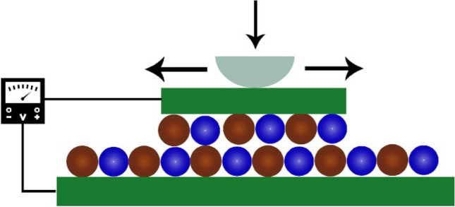
Schematic diagram of an InN-based compression-sliding motion nanogenerator model. The probe and electrodes are denoted by light cyan and green colors, respectively.
Our analysis and earlier studies on Au/2D-materials contact justify that the compression-sliding technique to be stable and resilient with the InN bilayer. The presence of the interlayer resistive force and sliding force converts mechanical energy into electrical energy. Thus, during the sliding process, tribological energy (Etribo) will contribute to the majority of the electrical energy (Eelec) production. If a conversion co-efficient (δ) is taken, then the amount of Eelec production can be found from the relation,
| 10 |
where P refers to the amount of electrical power generated from the nanogenerator at a certain time (t). Since the sliding force is provided to the model in a specific direction, the schematic configuration of Fig. 7 can further be investigated as a spring-force model66. If ∆Emax is the maximum sliding force barrier for one sliding cycle, then the amount of triboelectric energy and output electrical power per sliding cycle can be found by17,
| 11 |
| 12 |
where x and a are the sliding displacements per cycle and lattice constant, respectively. The power generated from the InN nanogenerator thus depends on the sliding velocity (x/t) and the height of the maximum sliding force barrier (∆Emax). When a higher sliding pressure is given to the model via the probe, the interlayer distance will decrease, and a higher output power will be obtained. In practice, the sliding velocity with the probe tips can range from 1 to 100 nm/s17. The power density coming from tribo-piezoelectricity can range from 738.22 to 73,822 μWcm−2 for the sliding velocity from 1 to 100 nm/s and the ∆Emax for the circumstance when the interlayer spacing is reduced to 2.51 Å, assuming that all the tribological energy converts to electrical energy. According to experimental observation11, a tribo-piezoelectric generator can provide a power density of 7 µWcm-2. Previous investigations have outlined the power density output from piezoelectric nanogenerators66 and triboelectric nanogenerators67 to be within the range of 4.41 to 5.92 μWcm−2 and 400 to 50,000 μWcm−2, respectively. The predicted InN bilayer nanogenerator shows a decent maximum power density and a considerable induced electrical output voltage, which is comparable to the theoretically and experimentally addressed triboelectric nanogenerators of Janus TMD bilayers17, GaN nanowire array68, h-BN polypropylene69, monolayer MoS2 flake70, and bilayer PVDF-TrFE and graphene oxide66, as outlined in Table 1.
Table 1.
Comparison of the maximum power density and induced voltage obtained from the proposed tribo-piezoelectric nanogenerator structure with previously investigated structures.
| Proposed material | Tribo-piezoelectric maximum power density (mWcm−2) | Peak induced output voltage (V) | ||
|---|---|---|---|---|
| Theoretical | Experimental | Theoretical | Experimental | |
| Proposed InN bilayer | ~ 73 | – | 0.196 | – |
| Janus TMD bilayers49 | ~ 29.64 | – | 0.25 | – |
| Monolayer MoS2 flake70 | – | ~ 2 × 10⁻⁴ | – | 0.015 |
| GaN nanowire array68 | – | – | – | 0.15–0.35 |
| h-BN polypropylene69 | – | ~ 29 × 10–4 | – | 2.3 |
| Bilayer PVDF-TrFE and graphene oxide66 | – | 4.41 × 10⁻³ | – | 4 |
Besides, we also extended our analysis by considering a 3 × 3 InN supercell bilayer structure that results in a power density of ~ 747.03 to 74,703 μWcm-2, which is slightly greater than the findings obtained with the InN unit cells. The induced voltage and polarization for the supercell structure are 0.148 V and 4.40 pC/m, respectively, whereas the values for the unit cell structure are 0.146 V and 4.38 pC/m. Thus, with increased surface area (large supercell structure), charge deviation increases, resulting in slightly higher induced voltage and maximum power density. Furthermore, a 10º and 5º twist on the upper InN layer has also been considered (Fig. 8). The maximum power density reaches to 713.58 μWcm-2 and 665.11 for the twist angles of 5º and 10º, respectively. The induced output voltage observed at 5º and 10º twists are ~ 0.108 and 0.100 V, respectively. Thus, a higher twist angle causes a reduction of induced voltage and maximum power density. As the twist angle increases (0º, 5º, and 10º), the polarization decreases (0.409, 0.408, and 0.404 pC/m, respectively), leading to the reduced induced voltage and power density.
Figure 8.

InN bilayer with upper layer is twisted at an angle of (a) 5° and (b) 10°. Here, the gray and cyan colors refer to N and In atoms, respectively.
The considered InN nanogenerator is a promising candidate in energy harvesting applications, especially for low-power electronics and self-powered sensors. In recent times, there have been tremendous improvements and investigations to fabricate InN based devices71, for instance, thin-film transistors72, lasers73, photovoltaic converters74, photodetectors75, and a number of terahertz-range devices76. Moreover, InN based nanowire77 and other structures78,79 are also getting improved day by day. Thus, the experimental fabrication of a 2D InN based tribo-piezoelectric nanogenerator is also expected to be feasible and sustainable in the near future.
Conclusions
In summary, the bilayer 2D InN structure is investigated to demonstrate the tribo-piezoelectric effect through first-principles calculations. For a fixed interlayer distance, in-plane sliding of the top InN layer results in a large out-of-plane vertical polarization. Instead of generating static charges, the tribological energy engenders piezoelectric polarization. The A–A stacking patterns result in a higher tribo-piezoelectric energy than the A–B stacking pattern. The amount of tribological energy depends on the magnitude of shear strength and interlayer sliding resistive force. The obtained induced voltage can be as high as ~ 0.2 V during vertical compressive sliding of the top plane. Moreover, a compressive-sliding motion nanogenerator structure is proposed. The nanogenerator can result in a tunable electrical output of 738.22 to 73,822 μWcm−2 by varying the pressure on its probe tip. These investigations strongly demonstrate that the InN bilayer could be a stable and highly efficient nanogenerator for energy conversion and energy harvesting.
Supplementary Information
Acknowledgements
This study was supported by the facilities of the UGC-funded research project (Grant No. CASR-55/23, 2020-2021), provided by the CASR at Khulna University of Engineering & Technology, Bangladesh.
Author contributions
M. S. I. conceived the work; M. Y. Z. and M. R. H. M. performed the simulations under the supervision of C. S. and J. P. All authors discussed and analyzed the data and interpretation and contributed during the writing of the manuscript.
Competing interests
The authors declare no competing interests.
Footnotes
Publisher's note
Springer Nature remains neutral with regard to jurisdictional claims in published maps and institutional affiliations.
Supplementary Information
The online version contains supplementary material available at 10.1038/s41598-021-98130-5.
References
- 1.Ganapathy SR, Salleh H, Azhar MKA. Design and optimisation of magnetically-tunable hybrid piezoelectric-triboelectric energy harvester. Sci. Rep. 2021;11:1–13. doi: 10.1038/s41598-021-83776-y. [DOI] [PMC free article] [PubMed] [Google Scholar]
- 2.Wang X, et al. A flexible triboelectric-piezoelectric hybrid nanogenerator based on P(VDF-TrFE) nanofibers and PDMS/MWCNT for wearable devices. Sci. Rep. 2016;6:1–10. doi: 10.1038/s41598-016-0001-8. [DOI] [PMC free article] [PubMed] [Google Scholar]
- 3.Wu T, et al. High-performance nanogenerators based on flexible cellulose nanofibril/MoS2 nanosheet composite piezoelectric films for energy harvesting. Nano Energy. 2021;80:105541. doi: 10.1016/j.nanoen.2020.105541. [DOI] [Google Scholar]
- 4.Lee P-C, et al. Development of porous ZnO thin films for enhancing piezoelectric nanogenerators and force sensors. Nano Energy. 2021;82:105702. doi: 10.1016/j.nanoen.2020.105702. [DOI] [Google Scholar]
- 5.Fan FR, Tang W, Wang ZL. Flexible nanogenerators for energy harvesting and self-powered electronics. Adv. Mater. 2016;28:4283–4305. doi: 10.1002/adma.201504299. [DOI] [PubMed] [Google Scholar]
- 6.Wang S, Lin L, Wang ZL. Nanoscale triboelectric-effect-enabled energy conversion for sustainably powering portable electronics. Nano Lett. 2012;12:6339–6346. doi: 10.1021/nl303573d. [DOI] [PubMed] [Google Scholar]
- 7.Lee G-J, et al. Piezoelectric energy harvesting from two-dimensional boron nitride nanoflakes. ACS Appl. Mater. Interfaces. 2019;11:37920–37926. doi: 10.1021/acsami.9b12187. [DOI] [PubMed] [Google Scholar]
- 8.Cherumannil Karumuthil S, Rajeev SP, Varghese S. Piezo-tribo nanoenergy harvester using hybrid polydimethyl siloxane based nanocomposite. Nano Energy. 2017;40:487–494. doi: 10.1016/j.nanoen.2017.08.052. [DOI] [Google Scholar]
- 9.Chen X, Xu S, Yao N, Shi Y. 1.6 V nanogenerator for mechanical energy harvesting using PZT nanofibers. Nano Lett. 2010;10:2133–2137. doi: 10.1021/nl100812k. [DOI] [PubMed] [Google Scholar]
- 10.Chang C, Tran VH, Wang J, Fuh YK, Lin L. Direct-write piezoelectric polymeric nanogenerator with high energy conversion efficiency. Nano Lett. 2010;10:726–731. doi: 10.1021/nl9040719. [DOI] [PubMed] [Google Scholar]
- 11.Yang X, Daoud WA. Triboelectric and piezoelectric effects in a combined tribo-piezoelectric nanogenerator based on an interfacial ZnO nanostructure. Adv. Funct. Mater. 2016;26:8194–8201. doi: 10.1002/adfm.201602529. [DOI] [Google Scholar]
- 12.Today, Z. W.-M. & 2017, undefined. On Maxwell’s Displacement Current for Energy and Sensors: The Origin of Nanogenerators (Elsevier, New York).
- 13.Zhu G, Yang R, Wang S, Wang ZL. Flexible high-output nanogenerator based on lateral ZnO nanowire array. Nano Lett. 2010;10:3151–3155. doi: 10.1021/nl101973h. [DOI] [PubMed] [Google Scholar]
- 14.Wang ZL, Song J. Piezoelectric nanogenerators based on zinc oxide nanowire arrays. Science. 2006;312:242–246. doi: 10.1126/science.1124005. [DOI] [PubMed] [Google Scholar]
- 15.Dong L, Lou J, Shenoy VB. Large in-plane and vertical piezoelectricity in janus transition metal dichalchogenides. ACS Nano. 2017;11:8242–8248. doi: 10.1021/acsnano.7b03313. [DOI] [PubMed] [Google Scholar]
- 16.Han SA, Lee J, Lin J, Kim S-W, Kim JH. Piezo/triboelectric nanogenerators based on 2-dimensional layered structure materials. Nano Energy. 2019;57:680–691. doi: 10.1016/j.nanoen.2018.12.081. [DOI] [Google Scholar]
- 17.Cai H, Guo Y, Gao H, Guo W. Tribo-piezoelectricity in Janus transition metal dichalcogenide bilayers: A first-principles study. Nano Energy. 2019;56:33–39. doi: 10.1016/j.nanoen.2018.11.027. [DOI] [Google Scholar]
- 18.Wang ZL. Triboelectric nanogenerators as new energy technology for self-powered systems and as active mechanical and chemical sensors. ACS Nano. 2013;7:9533–9557. doi: 10.1021/nn404614z. [DOI] [PubMed] [Google Scholar]
- 19.Zhang H, et al. Triboelectric nanogenerator as self-powered active sensors for detecting liquid/gaseous water/ethanol. Nano Energy. 2013;2:693–701. doi: 10.1016/j.nanoen.2013.08.004. [DOI] [Google Scholar]
- 20.Lin Wang, Z., Jun Chen, ab & Lin, L. Progress in triboelectric nanogenertors as new energy technology and self-powered sensors †. Energy Env. Sci. 1–10 (2014).
- 21.Wang S, et al. Sliding-triboelectric nanogenerators based on in-plane charge-separation mechanism. Nano Lett. 2013;13:2226–2233. doi: 10.1021/nl400738p. [DOI] [PubMed] [Google Scholar]
- 22.Zhu G, et al. Linear-grating triboelectric generator based on sliding electrification. Nano Lett. 2013;13:2282–2289. doi: 10.1021/nl4008985. [DOI] [PubMed] [Google Scholar]
- 23.Sheehan PE, Lieber CM. Friction between van der Waals solids during lattice directed sliding. Nano Lett. 2017;17:4116–4121. doi: 10.1021/acs.nanolett.7b00871. [DOI] [PubMed] [Google Scholar]
- 24.Chen A, Zhang C, Zhu G, Wang ZL. Polymer materials for high-performance triboelectric nanogenerators. Adv. Sci. 2020;7:2000186. doi: 10.1002/advs.202000186. [DOI] [PMC free article] [PubMed] [Google Scholar]
- 25.Rathore S, Sharma S, Swain BP, Ghadai RK. A critical review on triboelectric nanogenerator. IOP Conf. Ser. Mater. Sci. Eng. 2018;377:012186. doi: 10.1088/1757-899X/377/1/012186. [DOI] [Google Scholar]
- 26.Islam MdS, Mojumder MdRH, Ferdous N, Park J. Germanene/2D-SiC van der Waals heterobilayer: Structural features and tunable electronic properties. Mater. Today Commun. 2020 doi: 10.1016/j.mtcomm.2020.101718. [DOI] [Google Scholar]
- 27.Mojumder MRH, Islam MS, Park J. Germanene/2D-AlP van der Waals heterostructure: Tunable structural and electronic properties. AIP Adv. 2021;11:015126. doi: 10.1063/5.0023448. [DOI] [PubMed] [Google Scholar]
- 28.Xu M, Liang T, Shi M, Chen H. Graphene-like two-dimensional materials. Chem. Rev. 2013;113:3766–3798. doi: 10.1021/cr300263a. [DOI] [PubMed] [Google Scholar]
- 29.Butler SZ, et al. Progress, challenges, and opportunities in two-dimensional materials beyond graphene. ACS Nano. 2013;7:2898–2926. doi: 10.1021/nn400280c. [DOI] [PubMed] [Google Scholar]
- 30.Islam MS, Mia I, Ahammed S, Stampfl C, Park J. Exceptional in-plane and interfacial thermal transport in graphene/2D-SiC van der Waals heterostructures. Sci. Rep. 2020;10:22050. doi: 10.1038/s41598-020-78472-2. [DOI] [PMC free article] [PubMed] [Google Scholar]
- 31.Wang QH, Kalantar-Zadeh K, Kis A, Coleman JN, Strano MS. Electronics and optoelectronics of two-dimensional transition metal dichalcogenides. Nat. Nanotechnol. 2012;7:699–712. doi: 10.1038/nnano.2012.193. [DOI] [PubMed] [Google Scholar]
- 32.Patel A, Singh D, Sonvane Y, Thakor PB, Ahuja R. High Thermoelectric performance in two-dimensional janus monolayer material WS-X ( X = Se and Te) ACS Appl. Mater. Interfaces. 2020;12:46212–46219. doi: 10.1021/acsami.0c13960. [DOI] [PMC free article] [PubMed] [Google Scholar]
- 33.Al Balushi ZY, et al. The impact of graphene properties on GaN and AlN nucleation. Surf. Sci. 2012;634:81–88. doi: 10.1016/j.susc.2014.11.020. [DOI] [Google Scholar]
- 34.Wang, J., reports, Y. Z.-S. & 2016, undefined. Topologic connection between 2-D layered structures and 3-D diamond structures for conventional semiconductors. nature.com. [DOI] [PMC free article] [PubMed]
- 35.Song Y, et al. Robust microscale superlubricity in graphite/hexagonal boron nitride layered heterojunctions. Nat. Mater. 2018;17:894–899. doi: 10.1038/s41563-018-0144-z. [DOI] [PubMed] [Google Scholar]
- 36.Guo Y, Qiu J, Guo W. Reduction of interfacial friction in commensurate graphene/h-BN heterostructures by surface functionalization. Nanoscale. 2016;8:575–580. doi: 10.1039/C5NR05806F. [DOI] [PubMed] [Google Scholar]
- 37.Prete MS, et al. Giant excitonic absorption and emission in two-dimensional group-III nitrides. Sci. Rep. 2020;10:10719. doi: 10.1038/s41598-020-67667-2. [DOI] [PMC free article] [PubMed] [Google Scholar]
- 38.Chen C-Y, et al. Gallium Nitride Nanowire Based Nanogenerators and Light-Emitting Diodes. ACS Nano. 2012;6:5687–5692. doi: 10.1021/nn301814w. [DOI] [PubMed] [Google Scholar]
- 39.Gogneau N, et al. From single III-nitride nanowires to piezoelectric generators: New route for powering nomad electronics. Semicond. Sci. Technol. 2016;31:103002. doi: 10.1088/0268-1242/31/10/103002. [DOI] [Google Scholar]
- 40.Wang X, et al. Electricity generation based on one-dimensional group-III nitride nanomaterials. Adv. Mater. 2010;22:2155–2158. doi: 10.1002/adma.200903442. [DOI] [PubMed] [Google Scholar]
- 41.Nan Y, Tan D, Zhao J, Willatzen M, Wang ZL. Shape- and size dependent piezoelectric properties of monolayer hexagonal boron nitride nanosheets. Nanoscale Adv. 2020;2:470–477. doi: 10.1039/C9NA00643E. [DOI] [PMC free article] [PubMed] [Google Scholar]
- 42.Huang C-T, et al. Single-InN-nanowire nanogenerator with upto 1 V output voltage. Adv. Mater. 2010;22:4008–4013. doi: 10.1002/adma.201000981. [DOI] [PubMed] [Google Scholar]
- 43.Guo Y, Zhu H, Wang Q. Piezoelectric Effects in Surface-Engineered Two-Dimensional Group III Nitrides. ACS Appl. Mater. Interfaces. 2019;11:1033–1039. doi: 10.1021/acsami.8b17341. [DOI] [PubMed] [Google Scholar]
- 44.Zavabeti A, et al. Two-dimensional materials in large-areas: Synthesis, properties and applications. Nano-Micro Lett. 2020;12:66. doi: 10.1007/s40820-020-0402-x. [DOI] [PMC free article] [PubMed] [Google Scholar]
- 45.Bhuiyan AG, Hashimoto A, Yamamoto A. Indium nitride (InN): A review on growth, characterization, and properties. J. Appl. Phys. 2003;94:2779–2808. doi: 10.1063/1.1595135. [DOI] [Google Scholar]
- 46.Prete MS, Pulci O, Bechstedt F. Strong in- and out-of-plane excitons in two-dimensional InN nanosheets. Phys. Rev. B. 2018;98:235431. doi: 10.1103/PhysRevB.98.235431. [DOI] [Google Scholar]
- 47.Liang D, et al. Electronic and excitonic properties of two-dimensional and bulk InN crystals. RSC Adv. 2017;7:42455–42461. doi: 10.1039/C7RA07640A. [DOI] [Google Scholar]
- 48.Pan W, Dimakis E, Wang GT, Moustakas TD, Tsui DC. Two-dimensional electron gas in monolayer InN quantum wells. Appl. Phys. Lett. 2014;105:213503. doi: 10.1063/1.4902916. [DOI] [Google Scholar]
- 49.Giannozzi P, et al. Quantum ESPRESSO toward the exascale. J. Chem. Phys. 2020;152:154105. doi: 10.1063/5.0005082. [DOI] [PubMed] [Google Scholar]
- 50.Giannozzi P, et al. QUANTUM ESPRESSO: A modular and open-source software project for quantum simulations of materials. J. Phys. Condens. Matter. 2009;21:395502. doi: 10.1088/0953-8984/21/39/395502. [DOI] [PubMed] [Google Scholar]
- 51.Perdew JP, Burke K, Ernzerhof M. Generalized gradient approximation made simple. Phys. Rev. Lett. 1996;77:3865–3868. doi: 10.1103/PhysRevLett.77.3865. [DOI] [PubMed] [Google Scholar]
- 52.Kresse G, Joubert D. From ultrasoft pseudopotentials to the projector augmented-wave method. Phys. Rev. B. 1999;59:1758–1775. doi: 10.1103/PhysRevB.59.1758. [DOI] [Google Scholar]
- 53.Klimeš J, Bowler DR, Michaelides A. Chemical accuracy for the van der Waals density functional. J. Phys. Condens. Matter. 2009;22:022201. doi: 10.1088/0953-8984/22/2/022201. [DOI] [PubMed] [Google Scholar]
- 54.Klimeš J, Bowler DR, Michaelides A. Van der Waals density functionals applied to solids. Phys. Rev. B. 2011;83:195131. doi: 10.1103/PhysRevB.83.195131. [DOI] [Google Scholar]
- 55.Yuan D, Liao H, Hu W. Assessment of van der Waals inclusive density functional theory methods for adsorption and selective dehydrogenation of formic acid on Pt(111) surface. Phys. Chem. Chem. Phys. 2019;21:21049–21056. doi: 10.1039/C9CP03452H. [DOI] [PubMed] [Google Scholar]
- 56.Monkhorst HJ, Pack JD. Special points for Brillouin-zone integrations. Phys. Rev. B. 1976;13:5188–5192. doi: 10.1103/PhysRevB.13.5188. [DOI] [Google Scholar]
- 57.Şahin H, et al. Monolayer honeycomb structures of group-IV elements and III-V binary compounds: First-principles calculations. Phys. Rev. B. 2009;80:155453. doi: 10.1103/PhysRevB.80.155453. [DOI] [Google Scholar]
- 58.Ferdous N, Islam MdS, Park J, Hashimoto A. Tunable electronic properties in stanene and two dimensional silicon-carbide heterobilayer: A first principles investigation. AIP Adv. 2019;9:025120. doi: 10.1063/1.5066029. [DOI] [Google Scholar]
- 59.Rashid AS, et al. Widely tunable electronic properties in graphene/two-dimensional silicon carbide van der Waals heterostructures. J. Comput. Electron. 2019;18:836–845. doi: 10.1007/s10825-019-01351-1. [DOI] [Google Scholar]
- 60.Sarker JD, et al. Tunable electronic properties in bismuthene/2D silicon carbide van der Waals heterobilayer. Jpn. J. Appl. Phys. 2019;59:SCCC03. doi: 10.7567/1347-4065/ab48b5. [DOI] [Google Scholar]
- 61.Hassan MS, Islam MS, Park J. Silicene/ZnI2 van der Waals heterostructure: Tunable structural and electronic properties. Nanotechnology. 2021;32:305707. doi: 10.1088/1361-6528/abf9c6. [DOI] [PubMed] [Google Scholar]
- 62.Liu S-W, et al. Robust microscale superlubricity under high contact pressure enabled by graphene-coated microsphere. Nat. Commun. 2017;8:14029. doi: 10.1038/ncomms14029. [DOI] [PMC free article] [PubMed] [Google Scholar]
- 63.Li H, et al. Superlubricity between MoS2 Monolayers. Adv. Mater. 2017;29:1701474. doi: 10.1002/adma.201701474. [DOI] [PubMed] [Google Scholar]
- 64.Vu CC, et al. Observation of normal-force-independent superlubricity in mesoscopic graphite contacts. Phys. Rev. B. 2016;94:081405. doi: 10.1103/PhysRevB.94.081405. [DOI] [Google Scholar]
- 65.Liu J, et al. Direct-current triboelectricity generation by a sliding Schottky nanocontact on MoS 2 multilayers. Nat. Nanotechnol. 2018;13:112–116. doi: 10.1038/s41565-017-0019-5. [DOI] [PubMed] [Google Scholar]
- 66.Bhavanasi V, Kumar V, Parida K, Wang J, Lee PS. Enhanced piezoelectric energy harvesting performance of flexible PVDF-TrFE bilayer films with graphene oxide. ACS Appl. Mater. Interfaces. 2016;8:521–529. doi: 10.1021/acsami.5b09502. [DOI] [PubMed] [Google Scholar]
- 77.Wang S, et al. Maximum surface charge density for triboelectric nanogenerators achieved by ionized-air injection: Methodology and theoretical understanding. Adv. Mater. 2014;26:6720–6728. doi: 10.1002/adma.201402491. [DOI] [PubMed] [Google Scholar]
- 68.Huang C-T, et al. GaN nanowire arrays for high-output nanogenerators. J. Am. Chem. Soc. 2010;132:4766–4771. doi: 10.1021/ja909863a. [DOI] [PubMed] [Google Scholar]
- 69.Liu Y, Ping J, Ying Y. Recent progress in 2D-nanomaterial-based triboelectric nanogenerators. Adv. Funct. Mater. 2021;31:2009994. doi: 10.1002/adfm.202009994. [DOI] [Google Scholar]
- 70.Wu W, et al. Piezoelectricity of single-atomic-layer MoS 2 for energy conversion and piezotronics. Nature. 2014;514:470–474. doi: 10.1038/nature13792. [DOI] [PubMed] [Google Scholar]
- 71.Pécz B, et al. Indium Nitride at the 2D Limit. Adv. Mater. 2021;33:2006660. doi: 10.1002/adma.202006660. [DOI] [PMC free article] [PubMed] [Google Scholar]
- 72.Lye KS, Kobayashi A, Ueno K, Ohta J, Fujioka H. InN thin-film transistors fabricated on polymer sheets using pulsed sputtering deposition at room temperature. Appl. Phys. Lett. 2016;109:032106. doi: 10.1063/1.4959777. [DOI] [Google Scholar]
- 73.Andreev BA, et al. Towards the indium nitride laser: Obtaining infrared stimulated emission from planar monocrystalline InN structures. Sci. Rep. 2018;8:9454. doi: 10.1038/s41598-018-27911-2. [DOI] [PMC free article] [PubMed] [Google Scholar]
- 74.Aliberti P, et al. Effects of non-ideal energy selective contacts and experimental carrier cooling rate on the performance of an indium nitride based hot carrier solar cell. Appl. Phys. Lett. 2011;99:223507. doi: 10.1063/1.3663862. [DOI] [Google Scholar]
- 75.Hsu L-H, et al. InN-based heterojunction photodetector with extended infrared response. Opt. Express. 2015;23:31150–31162. doi: 10.1364/OE.23.031150. [DOI] [PubMed] [Google Scholar]
- 76.Liu H, et al. Ultrastrong terahertz emission from InN nanopyramids on single crystal ZnO substrates. Adv. Opt. Mater. 2017;5:1700178. doi: 10.1002/adom.201700178. [DOI] [Google Scholar]
- 77.Zhao S, Mi Z. Chapter eight—InN nanowires: Epitaxial growth, characterization, and device applications. In: Mi Z, Jagadish C, editors. Semiconductors and Semimetals. New York: Elsevier; 2017. pp. 267–304. [Google Scholar]
- 78.Gautam A, van Veggel FCJM. Synthesis of InN@SiO2 nanostructures and fabrication of blue LED devices. ACS Appl. Mater. Interfaces. 2012;4:3902–3909. doi: 10.1021/am300704g. [DOI] [PubMed] [Google Scholar]
- 79.Pearton SJ, et al. GaN, ZnO and InN nanowires and devices. J. Nanosci. Nanotechnol. 2008;8:99–110. doi: 10.1166/jnn.2008.N01. [DOI] [PubMed] [Google Scholar]
Associated Data
This section collects any data citations, data availability statements, or supplementary materials included in this article.