

Abstract
The crystal distortion such as lattice strain and defect located at the surfaces and grain boundaries induced by soft perovskite lattice highly determines the charge extraction‐transfer dynamics and recombination to cause an inferior efficiency of perovskite solar cells (PSCs). Herein, the authors propose a strategy to significantly reduce the superficial lattice tensile strain by means of incorporating an inorganic 2D Cl‐terminated Ti3C2 (Ti3C2Cl x ) MXene into the bulk and surface of CsPbBr3 film. Arising from the strong interaction between Cl atoms in Ti3C2Cl x and the under‐coordinated Pb2+ in CsPbBr3 lattice, the expanded perovskite lattice is compressed and confined to act as a lattice “tape”, in which the Pb—Cl bond plays a role of “glue” and the 2D Ti3C2 immobilizes the lattice. Finally, the defective surface is healed and a champion efficiency as high as 11.08% with an ultrahigh open‐circuit voltage up to 1.702 V is achieved on the best all‐inorganic CsPbBr3 PSC, which is so far the highest efficiency record for this kind of PSCs. Furthermore, the unencapsulated device demonstrates nearly unchanged performance under 80% relative humidity over 100 days and 85 °C over 30 days.
Keywords: all‐inorganic CsPbBr3 perovskite solar cells, interface solidification, long‐term stability, strain release, Ti3C2 MXene
Arising from the formation of strong Pb—Cl bonding, chlorine terminated Ti3C2Cl x MXenes are used as lattice “tape” to reduce the defects and release tensile strain located at interfaces and grain boundaries of CsPbBr3 perovskite film, achieving a champion efficiency up to 11.08% with an ultrahigh voltage of 1.702 V for CsPbBr3 perovskite solar cells.
1. Introduction
Organic–inorganic hybrid perovskite solar cells (PSCs) have made a forward step towards upcoming commercialization due to the rapid increase of power conversion efficiency (PCE) from initial 3.8% to reported 25.6%.[ 1 , 2 , 3 , 4 , 5 , 6 ] However, the inherent decomposition of perovskite lattice under external stimulus such as moisture, oxygen, light and heat is still a stability burden in this way. Aiming to address this issue, all‐inorganic CsPbX 3 (X = I−, Br−, or Cl−) perovskites have been gradually regarded as promising alternatives because of their superior environmental tolerances.[ 7 , 8 , 9 , 10 , 11 , 12 ] Among them, tri‐brominated CsPbBr3 perovskite presents the best weatherability regardless of their large bandgap around 2.3 eV comparing to I‐containing species,[ 13 ] demonstrating a great potential in semitransparent photovoltaics or high‐voltage required electronics owing to the ultrahigh theoretical voltage output around 2.0 V.[ 14 , 15 , 16 ] Up to date, the minimum PCE loss of inorganic CsPbBr3 PSC is still much higher than that of other devices because of the defective interfaces and grain boundaries induced open‐circuit voltage (V oc) deficit. As is well known, the soft feature of perovskite film allows for substantial distorted lattices during the phase conversion process under high temperature, which are mainly located at the superficial region and grain boundaries.[ 17 , 18 ] Apart from the popular positive under‐coordinated Pb2+ ions and negative Pb—X antisites (PbX 3 −), the expanded or compressed lattice (in other words, tensile or compressive strain) in this area also determines the carrier transfer and ion migration.[ 19 , 20 ] How to heal the defective nanostructure and to realize the surface solidification undoubtedly maximize the device PCE of PSC.
Great efforts have been made to heal the perovskite surfaces by regulating the terminations.[ 21 ] Inspired by the defect passivation in Si solar cells, many organic chemicals with functional groups such as pyridine, thiophene, and thiourea have been demonstrated to donate peripheral electrons to the under‐coordinated Pb2+ defects for an improved efficiency and stability based on Lewis acid‐base interaction.[ 22 , 23 ] Furthermore, the fabrication of “bone‐joint” configuration or soft layer by incorporating organic species with flexible chains can also effectively release the detrimental lattice strain.[ 24 , 25 ] However, the delicate character of organic molecules and their weak secondary bonding with perovskite lattice cause an inactivation under high temperature and longstanding light irradiation, which is incompatible with the all‐inorganic concept.[ 26 ] Although inorganic passivation materials such as PbSO4, PbS, metal halides, and oxides are employed to increase the performance of PSCs,[ 27 ] there is still no effective passivator to simultaneously reduce the above‐mentioned defects and control lattice strain. How to make defect‐free perovskite film by passivation‐engineering and strain‐engineering is of great importance to maximize the photovoltaic performances of all‐inorganic CsPbBr3 solar cells.
Arising from the strong electronic coupling, Cl atoms display superiority to thermodynamically stabilize the perovskite lattice and regulate the grain growth dynamics owing to the higher formation energy of Pb—Cl antisites at interface.[ 28 ] But the prevalent Cl‐containing additives are always ionized, and the excess cations will destroy the perovskite lattice and induce unnecessary recombination centers. In this fashion, the cation size should be precisely controlled to avoid the size mismatch induced steric effect. As is well known, the newly emerging MXenes are new family members of the 2D transition‐metal carbides/nitrides with metallic conductivity and easily regulated termination with different chemical groups. Similar to graphene, the MXenes are obtained from the corresponding MAX (M = Ti, Nb, Mo, V, W, etc.; X = C or N; A = Al, Ga, Si, etc.) phases by selective etching A element and replacing the termination with F, Cl, OH, etc., commonly denoted as Tx .[ 29 ] Previous reports have demonstrated that the Ti3C2 Tx MXene can effectively accelerate the charge extraction, enlarge grain size and increase the PCEs of PSCs.[ 30 , 31 ] However, it is still in lack of a better understanding on the lattice strain release and defect passivation for Ti3C2 Tx MXene tailored perovskite films. Herein, we report an inorganic Cl‐terminated Ti3C2 (Ti3C2Cl x ) MXene to fully heal the defective surfaces and grain boundaries of CsPbBr3 film. The best device achieves an efficiency as high as 11.08% with an ultrahigh V oc of 1.702 V, to the best of our knowledge, these data are to date the highest PCE and V oc records for the all‐inorganic CsPbBr3 PSCs. Apart from the strong passivation interaction between terminated Cl atoms and under‐coordinated Pb2+ ions and enlarged perovskite grain size, the bridging connection between Pb2+‐Cl‐Ti3C2 restricts the expansion of perovskite lattice to act as a lattice “tape” to reduce the tensile strain. As a result, the significantly reduced defect density in CsPbBr3 film allows for the stability advancement under persistent attack by 80% humidity or 85 °C in air for the device free of encapsulation.
2. Results and Discussion
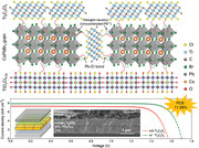
Cl‐terminated Ti3C2Cl x MXene is synthesized using a redox‐controlled Al etching of precursor Ti3AlC2 MAX‐phase in Lewis acidic CdCl2 melts combined with exfoliation and ultrasonication,[ 32 ] the details can be found in the Supporting Information. As schematically shown in Figure 1a , the unit cell of Ti3AlC2 MAX‐phase is composed of Ti6C octahedrons interleaved with layers of Al elements.[ 33 ] Upon selectively removing Al atoms from interlayers with CdCl2 melts, an accordion‐like microstructure (Figure S1, Supporting Information) demonstrates the formation of 2D MXene, which can be cross‐checked by X‐ray diffraction (XRD) patterns.[ 34 ] As shown in Figure 1b, most of the diffraction peaks of Ti3AlC2 MAX‐phase disappear in the final product, the characteristic diffraction peaks centered at 7.95°, 16.04°, 40.71°, and 57.98° correspond to the (002), (004), (10l), and (110) lattice planes of the Ti3C2 MXene,[ 32 , 35 ] respectively. Additionally, the disappearance of Al 2p signal and the appearance of a sharp peak of Cl 2p from X‐ray photoelectron spectroscopy (XPS) spectra (Figure 1c and Figures S2 and S3, Supporting Information) after etching treatment indicates the functional Cl termination on the Ti3C2Cl x MXene surface. The atomic ratio of Cl:Ti is determined to be 2:3 (11.69%:17.45%) based on the XPS results. The element mapping images (Figure S4, Supporting Information) also demonstrate the uniform distribution of Cl element on the surface of Ti3C2Cl x MXene. Through furiously mechanical liquid phase exfoliation, the delaminated Ti3C2Cl x MXene with thickness of ≈4 nm (Figure S5, Supporting Information) is obtained due to the weak interlayer van der Waals force. Arising from the ordered atom matrices with clear lattice fringes of defect‐free surface (Figure S6, Supporting Information), the as‐prepared Ti3C2Cl x MXene undoubtedly benefits the application in solar cells as lattice “tape” to regulate the chemical state of perovskite interfaces and grain boundaries.
Figure 1.

a) Schematic diagram of Ti3C2Cl x MXene preparation using Ti3AlC2 MAX in CdCl2 molten salt. b) XRD patterns of Ti3AlC2 MAX and Ti3C2Cl x MXene. c) XPS spectrum of Ti3C2Cl x MXene. d) The architecture and e) cross‐sectional SEM image of all‐inorganic PSC. f) J–V curves of control and optimized devices under reverse scan, g) steady power outputs, and h) IPCE spectra of PSCs. i) Statistical PCE distribution of pristine and optimal PSCs.
Subsequently, all‐inorganic CsPbBr3 PSC with a configuration of FTO/SnO2‐TiO x Cl4−2 x /CsPbBr3:Ti3C2Cl x / Ti3C2Cl x /carbon (Figure 1d) is fabricated by means of doping Ti3C2Cl x MXene into PbBr2 solution and spin‐coating Ti3C2Cl x onto the surface of final perovskite film. From the cross‐sectional scanning electron microscopy (SEM) image in Figure 1e, the device has a multilayered structure with a 60 nm SnO2‐TiO x Cl4−2 x layer, a 500 nm monolayer‐aligned perovskite overlayer and a 15 µm carbon electrode. By carefully optimizing the Ti3C2Cl x MXene dosage (Figure S7 and Table S1, Supporting Information), a champion PCE as high as 11.08% with an ultrahigh V oc of 1.702 V, a short‐circuit current density (J sc) of 7.87 mA cm−2, and a fill factor (FF) of 82.7% has been achieved by recording the characteristic photocurrent–voltage (J–V) curves via reverse scan under standard AM 1.5 G illumination, as shown in Figure 1f, which is much higher than that of pristine device with 9.18%‐efficiency. All the increased photovoltaic data including V oc, J sc, and FF are attributed to the reduction of charge recombination after adding Cl‐terminated Ti3C2 MXene.[ 36 ] To the best of our knowledge, both the PCE of 11.08% and V oc of 1.702 V are till now the highest records for state‐of‐the‐art all‐inorganic CsPbBr3 PSCs (Table S2, Supporting Information). The steady power outputs of inorganic CsPbBr3 PSCs under bias voltage at maximum power point (Figure 1g) and incident photon‐to‐current efficiency (IPCE) spectra (Figure 1h) are characterized to cross‐check the validity of PCE enhancement. A much higher steady efficiency of 11.0% and an increased integrated current density of 7.59 mA cm−2 for Ti3C2Cl x ‐tailored CsPbBr3 PSC from 6.90 mA cm−2 for control device demonstrate the validity of the above‐mentioned conclusion, highly agreeing well with the J–V measurements. Moreover, the hysteresis factor of devices has been reduced from 21.6% to 14.6% after the modification (Figure S8 and Table S3, Supporting Information). The statistical photovoltaic data of random 10 individual devices with and without Ti3C2Cl x modification also displays an obvious increase in PCE (Figure 1i) and other parameters (Figure S9, Supporting Information), further suggesting the positive effect of Ti3C2Cl x on solar‐to‐electric conversion. To highlight the superiority of Ti3C2 MXene in PSCs, we have also prepared F‐terminated Ti3C2F x and Br‐terminated Ti3C2Br x MXenes (Figure S10, Supporting Information) and a similar PCE enhancement is obtained after optimized the blending ratio of MXene (the optimized concentration is controlled at 0.02 mg mL−1, see Figure S11 and Table S4, Supporting Information). Taking the labile surface bonding of Cl/Br‐terminated MXene into consideration, versatile synthons for further chemical transformations provide multi‐possibilities to heal the defective surface of CsPbBr3 perovskite.
To reveal the intrinsic mechanism behind the efficiency enhancement, we first explore the effect of Ti3C2Cl x on the film quality. As shown in Figure 2a ,b and Figure S12, Supporting Information, the Ti3C2Cl x ‐tailored PbBr2 film with larger porosity is formed during the solvent volatilization.[ 37 ] These nanoholes undoubtedly provide enough pathways for subsequent CsBr diffusion and match pre‐expanded volume for perovskite grain growth,[ 38 ] helping make a high‐quality CsPbBr3 film with enlarged grain size and compact grain boundary (Figure 2c,d), which is accordance with the increased XRD peak intensities (Figure 2e) and enhanced light absorption ability (Figures S13 and S14, Supporting Information). The mechanism behind the regulated film growth dynamics is attributed to the stronger electronic coupling between Pb and Cl atoms (Figure S15, Supporting Information) than that with Br atoms. Upon introducing the Ti3C2Cl x into the perovskite precursor, partial PbBr2 lattice will bond with the dangling Cl atoms in Ti3C2Cl x to spatially retard the nucleation around the additives.[ 39 , 40 ] In the following phase conversion process from PbBr2 to CsPbBr3, the homogeneously distributed Ti3C2Cl x additives (Figures S16 and S17, Supporting Information) will play a role of “reservoir” to slow down the intercalation of Cs+ into underlying PbBr2 frameworks. Furthermore, the strong electron‐withdrawing properties of Cl atoms cause the binding energy of Pb 4f to shift up by 0.26 eV for Ti3C2Cl x ‐tailored CsPbBr3 (Figure 2f),[ 41 ] in other words, the electron cloud over under‐coordinated Pb2+ defect will be efficiently delocalized and redistributed over the whole lattice evenly, which in turn regulates the binding energies of Cs and Br elements (Figure S18, Supporting Information).[ 42 , 43 ] Similarly, the slight shifts of Cs 3d, Pb 4f, and Br 3d for the case of only Ti3C2Cl x surface modification also indicate the formation of Pb—Cl bonds at the CsPbBr3/Ti3C2Cl x interface (Figure S19, Supporting Information). Combined with the current results, we propose a concept of full defect passivation strategy here, as illustrated in Figure 2g, the strong binding interaction between under‐coordinated Pb2+ ions (V X ) and Cl atoms is responsible for the reduction of halide ions deficiency or excess induced defects due to the higher formation energy of Pb—Cl antisites at interfaces,.[ 44 ] It is worthy to mention that the underlying surface of perovskite film is passivated by the electron transfer layer SnO2/TiO x Cl4−2 x according to our previous report.[ 45 ]
Figure 2.

Top‐view SEM images of PbBr2 films and CsPbBr3 perovskite films a,c) without and b,d) with Ti3C2Cl x additive. e) XRD patterns and f) XPS spectra of Pb 4f for CsPbBr3 perovskite films. g) Schematic diagram of full defect passivation in CsPbBr3 film by Ti3C2Cl x MXene.
The surface lattices suffer from distortion to cause the formation of residual stress in perovskite film owing to the soft feature of perovskite, which is detrimental to device performance. Taking the stronger binding energy of Pb—Cl (301 kJ mol−1) in comparison to 248 kJ mol−1 for Pb—Br into consideration, the Cl terminated Ti3C2 MXene can drag the adjacent perovskite grains closer (reduced grain gap as shown in Figure 2d), anchoring the Pb atoms and confining the perovskite lattice without deformation owing to the immovable 2D Ti3C2 substrate. Following this line of thoughts, the Ti3C2Cl x is expected to be surface lattice “tape” to hinder the lattice expansion or contraction and reduce the residual stress. To deeply understand the strain evolution, we have characterized the Raman mapping images in Figure 3a ,b. In theory, the vibrational mode around 309 cm−1 in Raman spectra presents the reorientation of Cs+ in CsPbBr3 lattice influenced by the PbBr6 octahedral framework, which is strongly dependent on the lattice strain.[ 46 , 47 ] The enlarged lattice allows for a blue shift of Raman peak under the presence of tensile strain.[ 48 ] Therefore, the pristine CsPbBr3 perovskite film suffers from a serious tensile strain owing to the lower average wavenumber around 295 cm−1 for Cs+ vibrational mode in Figure 3c, which is mainly formed during the annealing process owing to the different thermal expansion coefficients of adjacent layers in the PSC devices.[ 49 ] Higher tensile strain results in more serious lattice distortion, larger charge transfer barrier, and lower ions migration energy.[ 50 ] Upon introducing Ti3C2Cl x MXene into the CsPbBr3 film, homogeneously distributed Raman peak for Cs+ vibrational mode is closer to 309 cm−1 (Figure 3b,c), this is a clear indicator of the released tensile strain in the perovskite film. We have further investigated the strain distribution by depth‐dependent grazing incident X‐ray diffraction (GIXRD) measurement to better highlight the lattice distortion in CsPbBr3 films. As shown in Figure 3d and Figure S20, Supporting Information, the obvious shift of the characteristic peaks for pristine perovskite film to lower angles along with increasing the incidence angle demonstrates gradually increased crystal plane distance along the perpendicular direction to substrate according to Bragg's Lawall, in other words, the pristine film suffers from a serious tensile strain. In contrast, the CsPbBr3 perovskite film with Ti3C2Cl x modification delivers a significantly reduced shift of diffraction peaks (Figure 3e and Figure S20, Supporting Information). The plots of d‐spacing values for (100) planes as a function of incident angle demonstrate the lattices across whole film especially in bottom region are contracted, as shown in Figure 3f. Owing to the strong electron‐withdrawing property of terminated Cl atoms to bond with under‐coordinated Pb2+ ion in the perovskite, 2D Ti3C2Cl x MXene can tightly adhere to the surface of CsPbBr3 grains, like a lattice “tape” to heal the soft perovskite lattice and to relieve the lattice expansion (Figure 3g,h).
Figure 3.

Raman mapping images of CsPbBr3 perovskite films a) without and b) with Ti3C2Cl x MXene, and c) the corresponding distribution statistics of Raman peak for different perovskite films. GIXRD patterns of CsPbBr3 (100) plane for the perovskite films d) without and e) with Ti3C2Cl x modification. f) d‐spacing values obtained from the GIXRD patterns as a function of the incidence angle. g) Schematic diagram of residual strain in the pristine CsPbBr3 grains, and h) schematic diagram of released strain in the reinforced CsPbBr3 grains with Ti3C2Cl x MXene.
Under light irradiation, the defects and strain in perovskite film will undoubtedly cause a carrier loss during the transfer process, as illustrated in Figure 4a , leaving less holes accumulated on the perovskite top surface. In this fashion, there will be more holes to call for a larger photovoltage upon healing and solidifying the defective surfaces and grain boundaries (Figure 4b). Aiming to visually distinguish the surface charge, we have further carried out transient surface photovoltage (TSPV) measurement and the schematic setup is provided in Figure S21, Supporting Information. As shown in Figure 4c, the higher positive signal of 7.36 V under pulse laser stimuli for Ti3C2Cl x ‐tailored perovskite film suggests an increased hole concentration,[ 51 ] which can be cross‐checked by the higher contact potential difference (CPD) than that of pristine perovskite film obtained from Kelvin probe force microscopy (KPFM) images (Figure 4d,e), therefore, the defects located at skin layer induced by dangling bonds and tensile strain are healed. We then quantitatively evaluated the defect‐state density (n t) in the perovskite films using a hole‐only device according to the space‐charge‐limited‐current (SCLC) model.[ 52 ] As shown in Figure 4f, the reduced trap‐filled limit voltage (V TFL) from 0.78 to 0.56 V for Ti3C2Cl x passivated perovskite film means a significantly reduced n t from 5.93 × 10¹⁵ to 1.92 × 1015 cm−3, which can be cross‐checked by the increased photoluminescence (PL) peak intensity (Figure S22, Supporting Information) because PL behavior of perovskite film is highly dependent on the defect density.[ 53 ] When assembled into a PSC, the nonradiative recombination is suppressed to produce a prolonged lifetime from 1.083 to 2.169 ns (Figure 4g and Table S5, Supporting Information) for a voltage and efficiency enhancement. As shown in Figure 4h, the reverse current density of optimized device under dark condition is over one order of magnitude lower than that of reference device, demonstrating that more photogenerated carriers pass through the device rather than direct shunting along with the defect‐assisted channels.[ 54 ] By further recording capacitance–voltage curves in the dark according to the Mott–Schottky relationship (Figure 4i), a higher built‐in electric field (V bi) for the Ti3C2Cl x ‐tailored PSC implies an enhanced driving force for charge separation (improved electron lifetime, see Figure S23, Supporting Information) and an extended depletion region for suppressing charge recombination (enlarged recombination resistance, see Figure S24, Supporting Information),[ 55 , 56 ] which is one main origin for the ultrahigh V oc. Apart from the reduced defect and the released strain, we have further characterized the band structure of MXene. As shown in Figure S25, Supporting Information, the work function of Ti3C2Cl x Mxene obtained from ultraviolet photoelectron spectroscopy (UPS) is deterimined to be −4.62 eV, which will upward bend the valence and conduction band of CsPbBr3 at the interface, accelerating the charge extraction.[ 57 ]
Figure 4.

Illustration for the photogenerated carrier transfer in a) pristine and b) Ti3C2Cl x containing perovskite films. c) TSPV curves of various PSCs. d) KPFM images and e) the corresponding CPD distributions of perovskite films. f) Dark J–V curves for the hole‐only devices with and without Ti3C2Cl x MXene. g) TRPL curves of perovskite films with and without Ti3C2Cl x . h) Dark J–V curves and i) Mott–Schottky curves of various PSCs.
Finally, the long‐term stability of all‐inorganic CsPbBr3 PSCs is evaluated under persistent moisture or thermal attacks. As shown in Figure 5a , the Ti3C2Cl x ‐repaired PSC device free of encapsulation delivers a stabilized PCE performance under 25 °C and 80% relative humidity (RH) in air over 100 days, which is mainly attributed to the reduced defect and contracted lattice to trigger unwanted phase attenuation and the protection of hydrophobic Ti3C2Cl x encapsulant (enlarged contact angle from 50.9° to 92.1°).[ 58 ] Owing to the absence of damageable organic species, both two PSCs present excellent thermal stability. As shown in Figure 5b, there is nearly no PCE degradation after 30 days storage under 85 °C, 40% RH condition, demonstrating the advantages of functionalized Ti3C2 as lattice “tape” to enhance the performance of highly‐efficient PSCs. It is worthy to note that the performance improvement behavior of PSC device in stability test is related to the film quality improvement after storage for a few days under controlled ambient atmosphere.[ 59 ]
Figure 5.

Long‐term stability of the encapsulation‐free devices with and without Ti3C2Cl x in air under a) 25 °C, 80% RH and b) 85 °C, 40% RH conditions.
3. Conclusions
In summary, we have demonstrated a novel strategy to simultaneously realize defect passivation and strain release by incorporating Cl‐terminated Ti3C2 MXene into the bulk and surface of perovskite film for stable and efficient all‐inorganic CsPbBr3 PSCs. Arising from the formation of Pb—Cl bond between the interfacial under‐coordinated Pb2+ ions in perovskite lattice and terminated Cl atoms in Ti3C2Cl x MXene, the defects and expanded lattices located at the interfaces and grain boundaries in perovskite film are significantly healed, playing a role of surface lattice “tape”, in which the Pb—Cl bond represents “glue” and Ti3C2 immobilizes the lattice. As a result, the best all‐inorganic CsPbBr3 PSC achieves an efficiency as high as 11.08% with an ultrahigh V oc of 1.702 V, which are the highest PCE and voltage records for CsPbBr3 solar cells. Moreover, the unencapsulated solar cell presents an excellent stability under high humidity (80% RH) and high temperature (85 °C) conditions over 100 and 30 days, respectively. Our findings open up a new avenue for preparing high‐quality defect‐free perovskite films, which not only benefits preparing high‐performance PSCs but also other optoelectronic devices based on perovskites.
4. Experimental Section
Materials and Reagents
SnCl2·2H2O (Alfa Aesar), CH4N2S (Macklin), TiCl4 (Aladdin), Ti3AlC2 (Mianyang Hengchuan Electrical Equipment Sales Co., Ltd.), PbBr2 (Aladdin), CsBr (Aladdin), N,N‐dimethylformamide (DMF, Sinopharm), CH3OH (Sinopharm), isopropanol (IPA, Aladdin), HCl (Guangzhou Chemical Reagent Factory), FTO glass (12 Ω per square), Zn powder (Guangzhou Chemical Reagent Factory), carbon paste (Shanghai MaterWin New Materials Co., Ltd). All materials were used as supplied without further treatment.
Synthesis of Ti3C2Cl x MXene
The Cl‐terminated Ti3C2 MXene was fabricated through molten salt‐based etching of Ti3AlC2 MAX phase and surface group substitution/elimination reactions in a N2‐filled glovebox.[ 35 ] 0.5 g of Ti3AlC2 was first mixed with 3.768 g of CdCl2 (molar ratio of 1:8). The resultant mixture was then heated in an alumina crucible at 610 °C for 7 h, which involved the following reactions.
| (1) |
| (2) |
After cooling to room temperature, the powders were washed by concentrated aqueous HCl (12.1 m) to remove excess CdCl2 and metallic Cd, followed by washing with deionized water for several times until pH ≈ 6.5. The resultant Cl functionalized MXene powders were dried under vacuum at 45 °C. Finally, by liquid phase exfoliation of Cl functionalized MXene powders in IPA, the 2D few‐layer Cl‐terminated Ti3C2Cl x MXene could be obtained. In details, 0.1 g of Cl functionalized MXene powders was added to 50 mL of IPA and then ultrasonicated for 25 h at a power of 300 W. The upper dark green suspension was obtained after centrifuging at 10 000 rpm for 30 min to separate the un‐exfoliated MXene. Before usage, the obtained Ti3C2Cl x MXene suspension was filtered with 0.22 µm PTFE filter.
Solar Cell Fabrication
The FTO‐coated glass was etched with Zn powders and HCl aqueous solution to obtain the desired pattern and then ultrasonic cleaned with detergent, deionized water, and ethanol. The cleaned FTO substrates were further treated by plasma for 5 min. Before deposition, FTO substrates and SnO2 QDs solution were preheated at 80 °C, in which SnO2 QDs solution was prepared according to our previous reports.[ 45 ] Compact SnO2 layer was deposited onto FTO substrate by spin‐coating at 2000 rpm for 30 s and subsequently annealed at 200 °C for 1 h in air. Then, TiCl4 treatment was performed by soaking the SnO2 coated FTO glass in TiCl4 aqueous solution (40 mm) at 75 °C for 30 min. After washed with deionized water and ethanol, the substrate was then annealed in air at 200 °C for 30 min. The CsPbBr3 film was fabricated by a multi‐step spin‐coating method. In details, 1 m PbBr2 DMF solution with different amount of Ti3C2Cl x was spin‐coated on the substrate at 2000 rpm for 30 s under 100 °C and then dried at 100 °C for 30 min. After that, 0.07 m CsBr methanol solution was spin‐coated onto PbBr2 film at 2000 rpm for 30 s, and heated at 250 °C for 5 min. By repeated this process for several times, a high quality CsPbBr3 film was obtained. 1 mg mL−1 Ti3C2Cl x suspension in IPA was spin‐coated on the surface of CsPbBr3 film at 2000 rpm for 30 s, and then annealed in air at 100 °C for another 5 min. Finally, a conductive carbon electrode with active area of 0.09 cm2 was coated on the perovskite film by a blade coating method.
Characterizations
The morphologies were obtained by a field emission SEM (Hitachi S4800) and transmission electron microscope (Tecnai G2 F20). The element analysis was carried out using SEM (FEI QUANTA250 and Zeiss Gemini300). The Raman mapping was recorded using an InVia Raman system (a42K864 Renishaw, InVia system) with an excitation laser wavelength of 532 nm. The film thickness of MXene was obtained by atomic force microscopy (AFM, Seiko SPA400). The surface potential was characterized by KPFM (Multimode 8, Bruker, German). The XRD and GIXRD patterns of perovskite and MXenes were conducted on an X‐ray diffractometer (Bruker D8 Advance). PL spectra were recorded via a fluorescence spectrometer excited by a 350 nm laser and the TRPL spectra were characterized using a Horiba spectrometer with an excitation wavelength of 500 nm. The characteristic J–V curves of PSCs were recorded on an electrochemical workstation (CHI660E) under irradiation of simulated solar light (Newport, Oriel Class 3A, 91195A). The light intensity was controlled at 100 mW cm−2 calibrated by a standard silicon solar cell. The IPCE spectra of various devices were obtained using an IPCE kit from Enli Technology Co., Ltd. The V oc decay curves were measured at open‐circuit mode by illuminating the device for several seconds, and then instantaneously switching off the light. The TSPV signals were recorded by a home‐made setup using a 355 nm laser. Capacitance–voltage (C–V) curves were measured at a frequency of 5 kHz with an amplitude of 5 mV under dark. Tafel curves of various devices were measured on CHI660E electrochemical workstation.
Conflict of Interest
The authors declare no conflict of interest.
Supporting information
Supporting Information
Acknowledgements
This work was supported by Guangdong Basic and Applied Basic Research Foundation (2020A1515110548), Guangzhou Basic and Applied Basic Research Foundation (202102020775), Postdoctoral Research Foundation of China (2020M683185, 2019M663379), National Natural Science Foundation of China (61774139, 62004083, U1802257), Natural Science Foundation of Guangdong Province (2019B151502061, 2020A1515011123), and the Fundamental Research Funds for the Central Universities (21620348, 21618409, 21619311).
Zhou Q., Duan J., Du J., Guo Q., Zhang Q., Yang X., Duan Y., Tang Q., Tailored Lattice “Tape” to Confine Tensile Interface for 11.08%‐Efficiency All‐Inorganic CsPbBr3 Perovskite Solar Cell with an Ultrahigh Voltage of 1.702 V. Adv. Sci. 2021, 8, 2101418. 10.1002/advs.202101418
Contributor Information
Jialong Duan, Email: duanjialong@jnu.edu.cn.
Qunwei Tang, Email: tangqunwei@jnu.edu.cn.
Data Availability Statement
Data sharing is not applicable to this article as no new data were created or analyzed in this study.
References
- 1. Kojima A., Teshima K., Shirai Y., Miyasaka T., J. Am. Chem. Soc. 2009, 131, 6050. [DOI] [PubMed] [Google Scholar]
- 2. Chen H., Ye F., Tang W., He J., Yin M., Wang Y., Xie F., Bi E., Yang X., Grätzel M., Han L., Nature 2017, 550, 92. [DOI] [PubMed] [Google Scholar]
- 3. Wang Y., Dar M. I., Ono L. K., Zhang T., Kan M., Li Y., Zhang L., Wang X., Yang Y., Gao X., Qi Y., Grätzel M., Zhao Y., Science 2019, 365, 591. [DOI] [PubMed] [Google Scholar]
- 4. Xu Y., Wang M., Lei Y., Ci Z., Jin Z., Adv. Energy Mater. 2020, 10, 2002558. [Google Scholar]
- 5. Peng J., Walter D., Ren Y., Tebyetekerwa M., Wu Y., Duong T., Lin Q., Li J., Lu T., Mahmud M. A., Lem O. L. C., Zhao S., Liu W., Liu Y., Shen H., Li L., Kremer F., Nguyen H. T., Choi D.‐Y., Weber K. J., Catchpole K. R., White T. P., Science 2021, 371, 390. [DOI] [PubMed] [Google Scholar]
- 6. Jeong J., Kim M., Seo J., Lu H., Ahlawat P., Mishra A., Yang Y., Hope M. A., Eickemeyer F. T., Kim M., Yoon Y. J., Choi I. W., Darwich B. P., Choi S. J., Jo Y., Lee J. H., Walker B., Zakeeruddin S. M., Emsley L., Rothlisberger U., Hagfeldt A., Kim D. S., Grätzel M., Kim J. Y., Nature 2021, 592, 381. [DOI] [PubMed] [Google Scholar]
- 7. Duan J., Zhao Y., He B., Tang Q., Angew. Chem., Int. Ed. 2018, 57, 3787. [DOI] [PubMed] [Google Scholar]
- 8. Wang Q., Jin Z., Chen D., Bai D., Bian H., Sun J., Zhu G., Wang G., Liu S. F., Adv. Energy Mater. 2018, 8, 1800007. [Google Scholar]
- 9. Zhu W., Zhang Z., Chai W., Zhang Q., Chen D., Lin Z., Chang J., Zhang J., Zhang C., Hao Y., ChemSusChem 2019, 12, 2318. [DOI] [PubMed] [Google Scholar]
- 10. Yan L., Xue Q., Liu M., Zhu Z., Tian J., Li Z., Chen Z., Chen Z., Yan H., Yip H.‐L., Cao Y., Adv. Mater. 2018, 30, 1802509. [DOI] [PubMed] [Google Scholar]
- 11. Bian H., Bai D., Jin Z., Wang K., Liang L., Wang H., Zhang J., Wang Q., (Frank) Liu S., Joule 2018, 2, 1500. [Google Scholar]
- 12. Li Z., Zhou F., Yao H., Ci Z., Yang Z., Jin Z., Mater. Today 2021, 10.1016/j.mattod.2021.01.028. [DOI] [Google Scholar]
- 13. Zhang J., Hodes G., Jin Z., Liu S. F., Angew. Chem., Int. Ed. 2019, 58, 15596. [DOI] [PubMed] [Google Scholar]
- 14. Liang J., Wang C., Wang Y., Xu Z., Lu Z., Ma Y., Zhu H., Hu Y., Xiao C., Yi X., Zhu G., Lv H., Ma L., Chen T., Tie Z., Jin Z., Liu J., J. Am. Chem. Soc. 2016, 138, 15829. [DOI] [PubMed] [Google Scholar]
- 15. Duan J., Hu T., Zhao Y., He B., Tang Q., Angew. Chem., Int. Ed. 2018, 57, 5746. [DOI] [PubMed] [Google Scholar]
- 16. Huang D., Xie P., Pan Z., Rao H., Zhong X., J. Mater. Chem. A 2019, 7, 22420. [Google Scholar]
- 17. Lin Y., Liu Y., Chen S., Wang S., Ni Z., Van Brackle C. H., Yang S., Zhao J., Yu Z., Dai X., Wang Q., Deng Y., Huang J., Energy Environ. Sci. 2021, 14, 1563. [Google Scholar]
- 18. Chu W., Saidi W. A., Zhao J., Prezhdo O. V., Angew. Chem., Int. Ed. 2020, 59, 6435. [DOI] [PubMed] [Google Scholar]
- 19. Zhu C., Niu X., Fu Y., Li N., Hu C., Chen Y., He X., Na G., Liu P., Zai H., Ge Y., Lu Y., Ke X., Bai Y., Yang S., Chen P., Li Y., Sui M., Zhang L., Zhou H., Chen Q., Nat. Commun. 2019, 10, 815. [DOI] [PMC free article] [PubMed] [Google Scholar]
- 20. Xue D.‐J., Hou Y., Liu S.‐C., Wei M., Chen B., Huang Z., Li Z., Sun B., Proppe A. H., Dong Y., Saidaminov M. I., Kelley S. O., Hu J.‐S., Sargent E. H., Nat. Commun. 2020, 11, 1514. [DOI] [PMC free article] [PubMed] [Google Scholar]
- 21. Bi S., Leng X., Li Y., Zheng Z., Zhang X., Zhang Y., Zhou H., Adv. Mater. 2019, 31, 1805708. [DOI] [PubMed] [Google Scholar]
- 22. Chen B., Rudd P. N., Yang S., Yuan Y., Huang J., Chem. Soc. Rev. 2019, 48, 3842. [DOI] [PubMed] [Google Scholar]
- 23. Gao F., Zhao Y., Zhang X., You J., Adv. Energy Mater. 2020, 10, 1902650. [Google Scholar]
- 24. Wang H., Zhu C., Liu L., Ma S., Liu P., Wu J., Shi C., Du Q., Hao Y., Xiang S., Chen H., Chen P., Bai Y., Zhou H., Li Y., Chen Q., Adv. Mater. 2019, 31, 1904408. [DOI] [PubMed] [Google Scholar]
- 25. Meng X., Cai Z., Zhang Y., Hu X., Xing Z., Huang Z., Huang Z., Cui Y., Hu T., Su M., Liao X., Zhang L., Wang F., Song Y., Chen Y., Nat. Commun. 2020, 11, 3016. [DOI] [PMC free article] [PubMed] [Google Scholar]
- 26. Zhang H., Wu Y., Shen C., Li E., Yan C., Zhang W., Tian H., Han L., Zhu W., Adv. Energy Mater. 2019, 9, 1803573. [Google Scholar]
- 27. Qi W., Zhou X., Li J., Cheng J., Li Y., Ko M. J., Zhao Y., Zhang X., Sci. Bull. 2020, 65, 2022. [DOI] [PubMed] [Google Scholar]
- 28. Zhu P., Gu S., Luo X., Gao Y., Li S., Zhu J., Tan H., Adv. Energy Mater. 2019, 10, 1903083. [Google Scholar]
- 29. Naguib M., Mashtalir O., Carle J., Presser V., Lu J., Hultman L., Gogotsi Y., Barsoum M. W., ACS Nano 2012, 6, 1322. [DOI] [PubMed] [Google Scholar]
- 30. Yang L., Dall'Agnese C., Dall'Agnese Y., Chen G., Gao Y., Sanehira Y., Jena A. K., Wang X., Gogotsi Y., Miyasaka T., Adv. Funct. Mater. 2019, 29, 1905694. [Google Scholar]
- 31. Chen X., Xu W., Ding N., Ji Y., Pan G., Zhu J., Zhou D., Wu Y., Chen C., Song H., Adv. Funct. Mater. 2020, 30, 2003295. [Google Scholar]
- 32. Li Y., Shao H., Lin Z., Lu J., Liu L., Duployer B., Persson P. O. Å., Eklund P., Hultman L., Li M., Chen K., Zha X.‐H., Du S., Rozier P., Chai Z., Raymundo‐Piñero E., Taberna P.‐L., Simon P., Huang Q., Nat. Mater. 2020, 19, 894. [DOI] [PubMed] [Google Scholar]
- 33. Naguib M., Kurtoglu M., Presser V., Lu J., Niu J., Heon M., Hultman L., Gogotsi Y., Barsoum M. W., Adv. Mater. 2011, 23, 4248. [DOI] [PubMed] [Google Scholar]
- 34. Li M., Lu J., Luo K., Li Y., Chang K., Chen K., Zhou J., Rosen J., Hultman L., Eklund P., Persson P. O. Å., Du S., Chai Z., Huang Z., Huang Q., J. Am. Chem. Soc. 2019, 141, 4730. [DOI] [PubMed] [Google Scholar]
- 35. Kamysbayev V., Filatov A. S., Hu H., Rui X., Lagunas F., Wang D., Klie R. F., Talapin D. V., Science 2020, 369, 979. [DOI] [PubMed] [Google Scholar]
- 36. Tiep N. H., Ku Z., Fan H. J., Adv. Energy Mater. 2016, 6, 1501420. [Google Scholar]
- 37. Zhu L., Shi J., Lv S., Yang Y., Xu X., Xu Y., Xiao J., Wu H., Luo Y., Li D., Meng Q., Nano Energy 2015, 15, 540. [Google Scholar]
- 38. Zhao Y., Duan J., Wang Y., Yang X., Tang Q., Nano Energy 2020, 67, 104286. [Google Scholar]
- 39. Li S.‐S., Chang C.‐H., Wang Y.‐C., Lin C.‐W., Wang D.‐Y., Lin J.‐C., Chen C.‐C., Sheu H.‐S., Chia H.‐C., Wu W.‐R., Jeng U.‐S., Liang C.‐T., Sankar R., Chou F.‐C., Chen C.‐W., Energy Environ. Sci. 2016, 9, 1282. [Google Scholar]
- 40. Guo Z., Gao L., Xu Z., Teo S., Zhang C., Kamata Y., Hayase S., Ma T., Small 2018, 14, 1802738. [DOI] [PubMed] [Google Scholar]
- 41. Wang Y., Wu T., Barbaud J., Kong W., Cui D., Chen H., Yang X., Han L., Science 2019, 365, 687. [DOI] [PubMed] [Google Scholar]
- 42. Nam J. K., Chai S. U., Cha W., Choi Y. J., Kim W., Jung M. S., Kwon J., Kim D., Park J. H., Nano Lett. 2017, 17, 2028. [DOI] [PubMed] [Google Scholar]
- 43. Li Y., Duan J., Yuan H., Zhao Y., He B., Tang Q., Sol. RRL 2018, 2, 1800164. [Google Scholar]
- 44. Wang Y., Chen G., Ouyang D., He X., Li C., Ma R., Yin W., Choy W. C. H., Adv. Mater. 2020, 32, 2000186. [DOI] [PubMed] [Google Scholar]
- 45. Zhou Q., Duan J., Wang Y., Yang X., Tang Q., J. Energy Chem. 2020, 50, 1. [Google Scholar]
- 46. Cha J.‐H., Han J. H., Yin W., Park C., Park Y., Ahn T. K., Cho J. H., Jung D.‐Y., J. Phys. Chem. Lett. 2017, 8, 565. [DOI] [PubMed] [Google Scholar]
- 47. Ibaceta‐Jaña J., Muydinov R., Rosado P., Mirhosseini H., Chugh M., Nazarenko O., Dirin D. N., Heinrich D., Wagner M. R., Kühne T. D., Szyszka B., Kovalenko M. V., Hoffmann A., Phys. Chem. Chem. Phys. 2020, 22, 5604. [DOI] [PubMed] [Google Scholar]
- 48. Zhang L., Zeng Q., Wang K., J. Phys. Chem. Lett. 2017, 8, 3752. [DOI] [PubMed] [Google Scholar]
- 49. Zhao J., Deng Y., Wei H., Zheng X., Yu Z., Shao Y., Shield J. E., Huang J., Sci. Adv. 2017, 3, eaao5616. [DOI] [PMC free article] [PubMed] [Google Scholar]
- 50. Murali B., Yengel E., Peng W., Chen Z., Alias M. S., Alarousu E., Ooi B. S., Burlakov V., Goriely A., Eddaoudi M., Bakr O. M., Mohammed O. F., J. Phys. Chem. Lett. 2017, 8, 137. [DOI] [PubMed] [Google Scholar]
- 51. Qu N., Lei Y., Yang X., Hu X., Zhao W., Zhao C., Zheng Z., J. Mater. Chem. C 2020, 8, 8451. [Google Scholar]
- 52. Dong Q., Fang Y., Shao Y., Mulligan P., Qiu J., Cao L., Huang J., Science 2015, 347, 967. [DOI] [PubMed] [Google Scholar]
- 53. Yang S., Chen S., Mosconi E., Fang Y., Xiao X., Wang C., Zhou Y., Yu Z., Zhao J., Gao Y., De Angelis F., Huang J., Science 2019, 365, 473. [DOI] [PubMed] [Google Scholar]
- 54. Duan J., Zhao Y., Yang X., Wang Y., He B., Tang Q., Adv. Energy Mater. 2018, 8, 1802346. [Google Scholar]
- 55. Liu Z., Chang J., Lin Z., Zhou L., Yang Z., Chen D., Zhang C., Liu S. F., Hao Y., Adv. Energy Mater. 2018, 8, 1703432. [Google Scholar]
- 56. Ren Z., Wang J., Pan Z., Zhao K., Zhang H., Li Y., Zhao Y., Mora‐Sero I., Bisquert J., Zhong X., Chem. Mater. 2015, 27, 8398. [Google Scholar]
- 57. Chen T., Tong G., Xu E., Li H., Li P., Zhu Z., Tang J., Qi Y., Jiang Y., J. Mater. Chem. A 2019, 7, 20597. [Google Scholar]
- 58. Liu J., Zhang H.‐B., Sun R., Liu Y., Liu Z., Zhou A., Yu Z.‐Z., Adv. Mater. 2017, 29, 1702367. [Google Scholar]
- 59. Cho Y., Kim H. D., Zheng J., Bing J., Li Y., Zhang M., Green M. A., Wakamiya A., Huang S., Ohkita H., Ho‐Baillie A. W. Y., ACS Energy Lett. 2021, 6, 925. [Google Scholar]
Associated Data
This section collects any data citations, data availability statements, or supplementary materials included in this article.
Supplementary Materials
Supporting Information
Data Availability Statement
Data sharing is not applicable to this article as no new data were created or analyzed in this study.