

Abstract

The fabrication of a graphene–silicon (Gr-Si) junction involves the formation of a parallel metal–insulator–semiconductor (MIS) structure, which is often disregarded but plays an important role in the optoelectronic properties of the device. In this work, the transfer of graphene onto a patterned n-type Si substrate, covered by Si3N4, produces a Gr-Si device, in which the parallel MIS consists of a Gr-Si3N4-Si structure surrounding the Gr-Si junction. The Gr-Si device exhibits rectifying behavior with a rectification ratio up to 104. The investigation of its temperature behavior is necessary to accurately estimate the Schottky barrier height (SBH) at zero bias, φb0 = 0.24 eV, the effective Richardson’s constant, A* = 7 × 10⁻¹⁰ AK–2 cm–2, and the diode ideality factor n = 2.66 of the Gr-Si junction. The device is operated as a photodetector in both photocurrent and photovoltage mode in the visible and infrared (IR) spectral regions. A responsivity of up to 350 mA/W and an external quantum efficiency (EQE) of up to 75% are achieved in the 500–1200 nm wavelength range. Decreases in responsivity to 0.4 mA/W and EQE to 0.03% are observed above 1200 nm, which is in the IR region beyond the silicon optical band gap, in which photoexcitation is driven by graphene. Finally, a model based on two parallel and opposite diodes, one for the Gr-Si junction and the other for the Gr-Si3N4-Si MIS structure, is proposed to explain the electrical behavior of the Gr-Si device.
Keywords: graphene, Schottky diode, Gr-Si junction, heterojunction, photodetector, responsivity, visible, infrared, quantum efficiency, noise equivalent power
Introduction
Silicon has been leading the development of the semiconductor technology holding a dominant position in the microelectronics field for decades. However, silicon as an optoelectronic material suffers from the short bandwidth and the large surface reflectivity that limit the responsivity and the application of silicon-based photodetectors to near-infrared (NIR) bands. NIR photodetection, particularly at 1550 nm, is crucial for a variety of applications, ranging from optical communications1−3 to remote sensing.4−6
Graphene offers a very attractive platform for advanced optoelectronic applications due to its high conductivity, zero band gap, low noise, flexibility, chemical stability, and other extraordinary properties.7−10 Owing to its semimetal behavior and tunable energy Fermi level, it enables new functionalities in traditional electronic and optoelectronic devices.11,12 For instance, silicon can be joined to graphene to form a Schottky diode, which is used as a bias-controlled photodetector.12−15 Graphene can replace the metal contact of a Schottky junction and make shallow junctions with enhanced photoresponse.16,17 In reverse bias, photons with energy higher than the semiconductor band gap, absorbed in the semiconductor depletion layer, induce the formation of photocharges that are separated by the junction built-in field, originating a photocurrent. Moreover, photons with sub-band-gap energy can be adsorbed by graphene and inject electrons over the Gr-Si barrier, leading to a charge flow from the graphene to the semiconductor.17,18 Furthermore, the Gr-Si junction is a basic element for novel electronic devices for the integration of graphene into the existing semiconductor technology.19−21
A Gr-Si junction is fabricated on a Si substrate covered by a SiO2 dielectric layer, typically 100–300 nm thick or less. To increase the capacitance of the MIS structure, a thinner SiO2 layer down to 20 nm has been used.22 The etching of a window in the SiO2 cap layer exposes the Si area for the formation of the Gr-Si junction. The transferred graphene covers the bare Si area and encroaches upon the oxide layer for the formation of contacts with metal leads. Such an encroachment of graphene over SiO2 originates a MIS structure, namely, a Gr-SiO2-Si structure, which is in parallel with the Gr-Si junction. It has been shown that the MIS structure affects the current–voltage (IV) and capacitance–voltage characteristics of the junction23 and enhances its photodetection capability.24−26 The important role of the MIS structure has been pointed out by Riazimehr et al.,25,27 yet it is still neglected in several studies. In this work, we further point out that the MIS structure is essential to understand the electronic and optoelectronic properties of Gr-Si devices.
We transfer graphene monolayers, produced by chemical vapor deposition (CVD), onto a n-Si wafer covered by a patterned Si3N4 layer that replaces the traditional SiO2 dielectric. Si3N4 films are excellent diffusion barriers (for metal, water, oxygen, etc.) and have high dielectric constant (∼7.5) and dielectric strength (>107 V/cm). In such a way, we form Gr-Si junctions in parallel with Gr-Si3N4-Si MIS structures. The original use of Si3N4 instead of SiO2 allows us to enhance the MIS capacitance by increasing the dielectric constant and reducing the insulator thickness to 15 nm. We highlight the importance of the Gr-Si3N4-Si MIS capacitor as part of the Gr-Si device. The MIS capacitor plays a significant role in improving the optical and electronic properties of Gr-Si photodiodes, as reported in recent studies.25,27−29 Our special layout leads to the observation of unreported features, namely, a kink in the reverse-bias IV characteristics, which we attribute to Fowler–Nordheim (FN) tunneling and model as two parallel and opposite diodes. We demonstrate that the Gr-Si3N4-Si structure is a booster for the photoresponse as it becomes the reservoir of photogenerated holes that contribute to the photocurrent in reverse bias. Photogenerated holes accumulated at the Si3N4-Si interface that tunnel through the Si3N4 by the FN mechanism increase the photocurrent and enhance the responsivity of the device.
We evaluate transport parameters such as Gr-Si SBH and ideality factor, and we study the responsivity of the device in the visible and near-infrared regions demonstrating a promising photodetector. We show that the investigation of the temperature behavior of the Gr/Si device is necessary to accurately evaluate the SBH at zero bias and that the approach based on a single room-temperature I–V curve, although very common, leads to a substantial overestimation of the barrier height.
Our results can be adapted to other devices such as gated two-dimensional (2D)–2D heterojunctions or transparent conductive materials on three-dimensional (3D) semiconductors.
Materials and Methods
Samples were prepared on doped n-Si (100) wafers with a resistivity of ∼10 Ωcm, corresponding to a phosphorus dopant density of ∼4.5 × 1014 cm–3. A 15 nm thick silicon nitride (Si3N4) was deposited by CVD. Then, a 3 × 3 mm2 trench was patterned by lithography and wet etching of the silicon nitride. The trench area was further cleaned by hydrofluoric acid immediately before the Gr deposition to prevent or limit the formation of native oxide.
An ∼5 × 7 mm2 Gr sheet was transferred onto the Si substrates by a wet method (the details are reported elsewhere30) to cover the Si trench while extending over the surrounding Si3N4 layer, thus acting both as the anode of the Gr-Si junction and the top (gate) electrode of the Gr-Si3N4-Si MIS structure. Contacts to graphene were realized by Ag paste of about 1 mm diameter. The achievement of low-resistance ohmic contacts with graphene31 was verified by measuring linear IV characteristics between Ag-Gr contacts in two-probe configuration. Likewise, the Ag paste was spread on the scratched backside of the Si substrate to guarantee an ohmic back contact.
The schematic of the device is reported in Figure 1a. The Raman spectrum (Figure 1b) provides a clear evidence of a high-quality monolayer Gr layer, confirmed by the high-2D/G-intensity peak ratio and the negligible defect-related D-peak (∼1350 cm–1).
Figure 1.
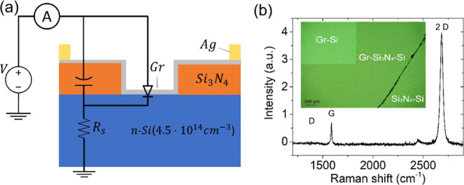
(a) Schematic of the device showing a Gr-Si junction modeled by a diode in parallel with a MIS structure, here represented as a capacitor. (b) Raman spectrum confirming high-quality monolayer graphene. The inset shows an optical top image of the device, displaying the graphene flake and the window etched through the Si3N4 layer corresponding to the Gr-Si junction.
Results and Discussion
Figure 2a shows the semilogarithmic plot of the IV characteristic of the Gr-Si device in the dark at 300 K and atmospheric pressure. The device exhibits a rectifying behavior with rectification ratio ∼104 at V = ±2.5 V and shape that suggests the use of the diode equation for the current
| 1 |
where I0 is the reverse saturation current, q is the electron charge, n is the ideality factor, k is the Boltzmann constant, and T is the temperature. The ideality factor considers deviations from pure thermoelectric transport (n = 1), which can take place in a Schottky diode. The presence of defects or unwanted insulating layers can cause Schottky barrier inhomogeneities and increase the ideality factor.32−34 The green dashed line in Figure 2a represents the fit to the experimental data of eq 1 with I0 and n as fitting parameters, obtained in the forward region 0 < V < 0.4 V. Indeed, in this region, any series resistance can be neglected, and the best fit is obtained with n = 2.02 and I0 = 1.69 × 10⁻⁹ A. Using the estimated value of I0 and referring to the thermionic theory
| 2 |
where S = 0.09 cm2 is the area of the junction, A* = 112 cm–2 K–2 is the Richardson constant for n-Si, and φb0 is the SBH at zero voltage. This estimation is affected by an error, which is related to the arbitrary choice of the forward region for the fit and might contain a huge systematic error due to the assumed values of S and A* (see below).
Figure 2.

(a) Measured IV characteristic of the device in the dark (black line). The green and magenta lines represent the fit using, respectively, eqs 1 and 3. Red and orange lines represent the fit using eq 6 with Cheung and Richardson’s parameters, respectively. The inset represents the diode model with a series and a parallel resistance corresponding to eq 6. (b) Cheung’s method plots for the evaluation of Schottky barrier height, ideality factor, and series resistance.
A more realistic model includes a series resistance Rs. We then follow Cheung’s method35 for evaluating the diode parameters. According to Cheung’s method, eq 1 with a series resistance becomes
| 3 |
which, for V – RsI ≫ nkT/q, provides
| 4 |
From the fit of eq 3, we can evaluate Rs and n, which can be used to estimate φb0, defining the following function
| 5 |
Figure 2b shows the plots
of  and H(I) as a
function of I from which we extract the following
parameters: n = 2.8, Rs = 85 kΩ, and φb0 = 0.87 eV. Using the so-estimated I0, Rs, and n in eq 3,
we obtain the magenta dotted curve shown in Figure 2a. Such a curve provides a good fit to the
forward current until the flat band condition is reached (V – RsI ≃ 0, which occurs at V ≃ 0.59 V),
where the diode equation does not apply anymore.
and H(I) as a
function of I from which we extract the following
parameters: n = 2.8, Rs = 85 kΩ, and φb0 = 0.87 eV. Using the so-estimated I0, Rs, and n in eq 3,
we obtain the magenta dotted curve shown in Figure 2a. Such a curve provides a good fit to the
forward current until the flat band condition is reached (V – RsI ≃ 0, which occurs at V ≃ 0.59 V),
where the diode equation does not apply anymore.
As all fittings fail in the reverse region, we further improve the model by considering a parallel resistance Rp, which takes into account possible leakages through the dielectric or the substrate edge24
| 6 |
Equation 6 provides an acceptable fit both in reverse and forward biases, as shown by the red dash-dot line in Figure 2a, when Rp = 4 MΩ and I0 = 2.3 ×10⁻⁸ A.
Figure 3a,b displays the IV characteristics of the Gr-Si device at different temperatures, from T = 400 to 220 K, in the dark and under illumination by a supercontinuum laser with a 3 mm diameter spot (incident power 1 mW/cm2, wavelength λ = 500 nm), respectively. The plots show that lowering the temperature suppresses both the forward and reverse currents, as predicted by the thermionic theory (eqs 1 and 2). Noteworthy is a substantial difference between the current in the dark and under illumination is observed only at temperatures below 320 K and in reverse bias. Light does not appreciably change the forward current and, at higher temperatures, the reverse current. At low temperatures, the IV curves present sudden curvature changes (one or more kinks) in reverse bias probably caused by the parallel MIS capacitor, as explained below.
Figure 3.

IV characteristics versus temperature ranging from 400 to 220 K (a) in the dark and (b) under light (3 mm diameter spot, incident power 1 mW/cm2, wavelength λ = 500 nm). (c) Rectification ratio at V = ±2.5 V, (d) ideality factor, (e) series resistance, and (f) Schottky barrier height versus temperature, estimated using Cheung’s method.
Figure 3c shows the rectification ratio at V = ±2.5 V. In the dark, the rectification ratio increases with decreasing temperature, indicating that the Schottky barrier becomes more efficient in suppressing the electron flow from graphene to silicon (reverse current) when the temperature is lowered. Under illumination, the rectification ratio overlaps that measured in the dark for temperatures higher than 320 K, i.e., when thermal generation overcomes photogeneration. Below 320 K, the rectification ratio decreases with decreasing temperature because the reverse current becomes more and more dominated by the photogeneration. This result indicates that the suppressed dark (reverse) current at a low temperature is favorable to photodetection. Indeed, at low temperatures, the reverse current is substantially enhanced by the electron–hole photogeneration.
From Cheung’s method, we obtained the values of n, Rs, and φb0 as a function of temperature, respectively, reported in Figure 3d–f, in the dark (black dot-lines) and under light (red dot-lines). The temperature dependence of the ideality factor in Figure 3d shows a descending behavior for increasing temperature. This feature indicates that deviations from the ideal thermionic behavior of the diode are more effective at lower temperatures when thermionic emission is suppressed, and tunneling and diffusion might become comparatively relevant. The dependence on the temperature of the series resistance is typical of a semiconductor and is probably dominated by the silicon substrate.
Finally, Figure 3f shows that the SBH increases with increasing temperature. This is a well-known effect when there is barrier inhomogeneity.36−38 At low temperatures, the reduced thermal energy makes the carrier cross the barrier mainly in the position where the SBH is lower, thus resulting in a reduced SBH.
The obtained zero-bias SBH, φb0 = 0.87 eV, although
consistent with some previous works,39,40 exceeds the
prediction of the Schottky–Mott model, φb0 = Φg – χSi = 0.5 eV (Φg = 4.54 eV is the commonly used work function of graphene
and χSi = 4.05 eV is the electronic affinity of Si)
and should result in lower reverse current and higher rectification
ratio than the ones we observed. We note that a large discrepancy
can be found in the literature for the Gr-Si SBH (from 0.2 to 0.9
eV24,39−45) estimated from electrical transport and that complementary techniques
such as X-ray photoemission spectroscopy lead to much lower barrier
height.43 Furthermore, several experimental
studies of the Gr-Si Schottky junction have indicated that an effective
Richardson constant, order of magnitude lower than 112 A cm–2 K–2, is needed to account for the experimental
data.21,23,36,37,46,47 Therefore, to make an estimation of the SBH independent of the effective
Richardson constant A* and to avoid relying on a
single IV curve, we extracted the SBH and, as byproduct,
the effective Richardson constant from the IV characteristics
measured at different temperatures (Figure 3a,b). The linear fittings of the forward
current were used to extrapolate the current I0 at V = 0 V, as shown in Figure 4a,b. According to eq 2, φb0 and A* can be obtained from the slope and intercept of ln (I0/T2) versus  (Richardson’s
plot in Figure 4c,d).
The estimated A* ≈ 7 × 10⁻¹⁰ A cm–2 K–2 is significantly
lower than the theoretical
one (112 A cm–2 K–2) used for
previous calculations, and the obtained SBH reduces to φb0 = 0.24 eV, consistent with the modest rectification ratio
and the results from similar devices.21,23,36,41,48,49 Although the origin of a lower
effective Richardson constant is still under debate,18,50 the inadvertent presence of a native oxide layer at Gr-Si interface,24 the massless Dirac fermion nature of carriers
in graphene,13 and a Landauer transport
mechanism46 have been invoked as an explanation.
We point out that the SBH does not change when measured in the dark
or under illumination. This is due to the negligible effects of light
on the forward IV characteristics of the device.
The I0 value obtained by eq 2 with φb0 and A* from Richardson’s plot, inserted in eq 6, provide the best fit to the data,
as shown by orange dash-dot line in Figure 2a (the other fitting parameters are Rp = 12 MΩ, I0 = 5.85 × 10⁻⁹ A). The excellent agreement
between experimental data and model is taken as a confirmation of
the higher accuracy of the Richardson plot-based method.
(Richardson’s
plot in Figure 4c,d).
The estimated A* ≈ 7 × 10⁻¹⁰ A cm–2 K–2 is significantly
lower than the theoretical
one (112 A cm–2 K–2) used for
previous calculations, and the obtained SBH reduces to φb0 = 0.24 eV, consistent with the modest rectification ratio
and the results from similar devices.21,23,36,41,48,49 Although the origin of a lower
effective Richardson constant is still under debate,18,50 the inadvertent presence of a native oxide layer at Gr-Si interface,24 the massless Dirac fermion nature of carriers
in graphene,13 and a Landauer transport
mechanism46 have been invoked as an explanation.
We point out that the SBH does not change when measured in the dark
or under illumination. This is due to the negligible effects of light
on the forward IV characteristics of the device.
The I0 value obtained by eq 2 with φb0 and A* from Richardson’s plot, inserted in eq 6, provide the best fit to the data,
as shown by orange dash-dot line in Figure 2a (the other fitting parameters are Rp = 12 MΩ, I0 = 5.85 × 10⁻⁹ A). The excellent agreement
between experimental data and model is taken as a confirmation of
the higher accuracy of the Richardson plot-based method.
Figure 4.

Linear fits used to extract I0 at V = 0 V (a) in the dark and (b) under illumination light (3 mm diameter spot, incident power 1 mW/cm2, wavelength λ = 500 nm). Richardson’s plots obtained from IV measurements (c) in the dark and (d) under illumination.
To further investigate the physical mechanisms of charge transport, we tested the optical response of the device. Figure 5a shows the IV characteristics in the dark and under illumination by a supercontinuum white laser. Tuning the emission power of the laser from 0 to 180 mW (corresponding to the integral intensity of 0–240 mW/cm2 on the device and considering a light loss factor of 85% in our measurement setup over the entire spectral range), we obtained the photoresponse of the device, defined as (Ilight – Idark)/Idark at V = −2.5 V, as shown in Figure 5b. The data follow an exponential law with the e-folding factor x0 = 56 mW, which ensures that a maximum light effect is reached above ∼170 mW with unfiltered laser light. Accordingly, the laser was set to a maximum power of 180 mW for further tests of the Gr-Si device in photocurrent and photovoltage mode.
Figure 5.

(a) IV characteristics in the dark and with incident white laser. (b) Photoresponse as a function of the laser emitted power and the laser integral intensity incident on the device (in mW/cm2). (c) Photocurrent when the photodetector is operated in the photocurrent mode at V = −2.5 V and (d) photovoltage mode at I = 0 A under a laser beam with 1000 nm wavelength and 950 μW/cm2 light intensity on the device.
Setting the voltage to V = −2.5 V, we performed a series of measurements exposing it to the laser beam with wavelength emission of λ = 1000 nm, as representative of NIR light above the silicon band gap. The device reacts to the laser with fast and repeatable photocurrent (Figure 5c). Furthermore, at zero current, we also observed a photovoltaic effect as reported in Figure 5d, where a voltage of about 12 mV appears at the electrode in response to a laser pulse. Due to the low incident power (950 μW/cm2), possible thermal effects can be excluded. Figure 5c,d shows that under illumination, the device generates both a current and a voltage, i.e., it can be operated in a self-powered mode, consistent with other works in the literature.51−53
To complete the
optoelectronic characterization of the device,
we investigated the spectral response in the 500–2000 nm wavelength
range by sampling the spectrum of the supercontinuum laser in intervals
of 50 and 20 nm bandwidth. Figure 6a reports the responsivity of the device, defined as
the ratio of photocurrent to the incident power, R = (Ilight – Idark)/Pinc(λ) along
with external quantum efficiency  (λ is the wavelength, h is Planck’s constant, and c is the speed
of light). It shows an EQE around 75% for λ < 1100 nm, i.e.,
when photoconversion occurs mainly in Si, followed by a sudden drop
to 0.03% when the energy of the incident light is below the band gap
of Si. For λ > 1100 nm, photoexcitation occurs mainly in
graphene
and the EQE, as reported elsewhere.9,54,55 We highlight that the obtained external quantum efficiency
is consistent with the highest value reported in the literature over
the investigated spectral range.22,53,56−60
(λ is the wavelength, h is Planck’s constant, and c is the speed
of light). It shows an EQE around 75% for λ < 1100 nm, i.e.,
when photoconversion occurs mainly in Si, followed by a sudden drop
to 0.03% when the energy of the incident light is below the band gap
of Si. For λ > 1100 nm, photoexcitation occurs mainly in
graphene
and the EQE, as reported elsewhere.9,54,55 We highlight that the obtained external quantum efficiency
is consistent with the highest value reported in the literature over
the investigated spectral range.22,53,56−60
Figure 6.

(a) Responsivity and EQE of the device in the visible and IR spectral regions. (b) NEP and (c) IV characteristics in the dark and under light at different wavelengths in the (c) visible and (d) near-spectral IR regions. The insets in (c) and (d) show the Fowler–Nordheim plots of the reverse IV characteristic at 550 and 850 nm, respectively.
As an additional figure of merit, Figure 6b shows the noise equivalent
power  that indicates the minimum detectable power.
Obviously, the higher quantum efficiency corresponds to the lower
detection power.
that indicates the minimum detectable power.
Obviously, the higher quantum efficiency corresponds to the lower
detection power.
Figure 6c,d shows the IV characteristics under light at different wavelengths. It can be observed that a kink forms at about V = −1.2 V in the reverse curves. The photocurrent at a given illumination and wavelength reaches a plateau at a high reverse bias when it is limited by the photocarrier generation rate.
The observed optoelectronic behavior of the Gr-Si device can be understood by considering the parallel Gr-Si3N4-n-Si structure, which in forward behaves like a MIS capacitor charged by an electron on the Si side. Such an electron can diffuse to the Gr-n-Si junction and contribute to the forward current. In reverse bias, the negative voltage attracts holes at the Si-Si3N4 interface. As the holes accumulate, the Si undergoes an inversion and becomes p-type. When the voltage is high enough to enable tunneling through the insulator, a p-type Schottky diode is formed in the MIS region. This means that, in reverse bias, the device behaves as two parallel and opposite diodes, a reverse Schottky diode due to the Gr-Si junction and a forward MIS diode formed by the Gr-Si3N4-p-Si structure. This parallel configuration explains the kinks at about V = −1.2 V. Indeed, for −1.2 V < V < 0 V, holes accumulated at the interface Si-Si3N4 can only diffuse toward the Gr-Si junction and contribute to its reverse current (Figure 7a), originating the leakage of ∼10–7 A. For V < −1.2 V, the electric field enables also FN tunneling61,62 through the Si3N4 layer (Figure 7b), resulting in an increase of current, which generates the aforementioned kinks. A current plateau is reached at a high reverse voltage because of the thermal or photogeneration-limited rate in Si. The FN tunneling mechanism is confirmed by the FN analysis of the reverse IV characteristics shown as insets in Figure 6c,d. Indeed, the linear behavior of the FN plot over the range –0.8 V–1 < V–1 < −0.5 V–1 (corresponding to −2.0 V to −1.25 V) demonstrates that FN tunneling occurs below the kink voltage.
Figure 7.

Schematic model of the Gr-Si device and charge carrier transport in reverse bias for (a) −1.2 V < V < 0 V and (b) V < −1.2 V.
Conclusions
We have studied a Schottky Gr-Si junction in parallel with a Gr-Si3N4-Si structure, forming a composite Gr-Si device with high responsivity and external quantum efficiency in the visible and NIR regions. The device can be operated in both photocurrent and photovoltage modes. We have evaluated the relevant parameters of the junction and shown that only a detailed IV–T analysis leads to a realistic estimation of the Gr-Si Schottky barrier parameters. We have detected the appearance of a kink in the reverse current, and we have proposed a model based on two parallel back-to-back diodes to explain it. We have clarified how the parallel Gr-Si3N4-Si structure introduced in the fabrication of the device contributes to the optoelectronic properties of the Gr/Si heterostructure.
Acknowledgments
A.D.B. thanks the University of Salerno, Salerno, Italy, for the grants ORSA200207 and ORSA195727.
Author Contributions
This manuscript was written through contributions of all authors. All authors have given approval to the final version of the manuscript.
The authors declare no competing financial interest.
References
- Ijaz M.; Ghassemlooy Z.; Rajbhandari S.; Minh H. L.; Perez J.; Gholami A. In Comparison of 830 Nm and 1550 Nm Based Free Space Optical Communications Link under Controlled Fog Conditions, 2012 8th International Symposium on Communication Systems, Networks Digital Signal Processing (CSNDSP), 2012; pp 1–5.
- Wang J.; Xing Z.; Chen X.; Cheng Z.; Li X.; Liu T. Recent Progress in Waveguide-Integrated Graphene Photonic Devices for Sensing and Communication Applications. Front. Phys. 2020, 8, 37 10.3389/fphy.2020.00037. [DOI] [Google Scholar]
- Zhou H.; Zhu X.; Gu T.; Wu J.; Deng G.; Huang S.-W.; Ophir N.; Yu M.; Kwong D.-L.; Zhou S.; Bergman K.; Wong C. W. Error-Free Data Transmission through Fast Broadband All-Optical Modulation in Graphene–Silicon Optoelectronics. Appl. Phys. Lett. 2020, 116, 221106 10.1063/5.0006596. [DOI] [Google Scholar]
- Blackett M. An Overview of Infrared Remote Sensing of Volcanic Activity. J. Imaging 2017, 3, 13. 10.3390/jimaging3020013. [DOI] [Google Scholar]
- Goddijn-Murphy L.; Williamson B. On Thermal Infrared Remote Sensing of Plastic Pollution in Natural Waters. Remote Sens. 2019, 11, 2159. 10.3390/rs11182159. [DOI] [Google Scholar]
- Hua L.; Shao G. The Progress of Operational Forest Fire Monitoring with Infrared Remote Sensing. J. For. Res. 2017, 28, 215–229. 10.1007/s11676-016-0361-8. [DOI] [Google Scholar]
- Geim A. K. Graphene: Status and Prospects. Science 2009, 324, 1530–1534. 10.1126/science.1158877. [DOI] [PubMed] [Google Scholar]
- Wang J.; Mu X.; Sun M.; Mu T. Optoelectronic Properties and Applications of Graphene-Based Hybrid Nanomaterials and van Der Waals Heterostructures. Appl. Mater. Today 2019, 16, 1–20. 10.1016/j.apmt.2019.03.006. [DOI] [Google Scholar]
- Luo F.; Zhu M.; tan Y.; Sun H.; Luo W.; Peng G.; Zhu Z.; Zhang X.-A.; Qin S. High Responsivity Graphene Photodetectors from Visible to Near-Infrared by Photogating Effect. AIP Adv. 2018, 8, 115106 10.1063/1.5054760. [DOI] [Google Scholar]
- Urban F.; Lupina G.; Grillo A.; Martucciello N.; Di Bartolomeo A. Contact Resistance and Mobility in Back-Gate Graphene Transistors. Nano Express 2020, 1, 010001 10.1088/2632-959X/ab7055. [DOI] [Google Scholar]
- Di Bartolomeo A.; Santandrea S.; Giubileo F.; Romeo F.; Petrosino M.; Citro R.; Barbara P.; Lupina G.; Schroeder T.; Rubino A. Effect of Back-Gate on Contact Resistance and on Channel Conductance in Graphene-Based Field-Effect Transistors. Diamond Relat. Mater. 2013, 38, 19–23. 10.1016/j.diamond.2013.06.002. [DOI] [Google Scholar]
- Di Bartolomeo A. Graphene Schottky Diodes: An Experimental Review of the Rectifying Graphene/Semiconductor Heterojunction. Phys. Rep. 2016, 606, 1–58. 10.1016/j.physrep.2015.10.003. [DOI] [Google Scholar]
- Liang S.-J.; Ang L. K. Electron Thermionic Emission from Graphene and a Thermionic Energy Converter. Phys. Rev. Appl. 2015, 3, 014002 10.1103/PhysRevApplied.3.014002. [DOI] [Google Scholar]
- Casalino M.; Sassi U.; Goykhman I.; Eiden A.; Lidorikis E.; Milana S.; De Fazio D.; Tomarchio F.; Iodice M.; Coppola G.; Ferrari A. C. Vertically Illuminated, Resonant Cavity Enhanced, Graphene–Silicon Schottky Photodetectors. ACS Nano 2017, 11, 10955–10963. 10.1021/acsnano.7b04792. [DOI] [PubMed] [Google Scholar]
- Alvarado Chavarin C.; Strobel C.; Kitzmann J.; Di Bartolomeo A.; Lukosius M.; Albert M.; Bartha J.; Wenger C. Current Modulation of a Heterojunction Structure by an Ultra-Thin Graphene Base Electrode. Materials 2018, 11, 345. 10.3390/ma11030345. [DOI] [PMC free article] [PubMed] [Google Scholar]
- Casalino M.; Crisci T.; Moretti L.; Gioffre M.; Iodice M.; Coppola G.; Maccagnani P.; Rizzoli R.; Bonafe F.; Summonte C.; Morandi V.. Silicon Meet Graphene for a New Family of Near-Infrared Resonant Cavity Enhanced Photodetectors, 2020 22nd International Conference on Transparent Optical Networks (ICTON), IEEE: Bari, Italy, 2020; pp 1–4.
- Di Bartolomeo A.; Luongo G.; Iemmo L.; Urban F.; Giubileo F. Graphene–Silicon Schottky Diodes for Photodetection. IEEE Trans. Nanotechnol. 2018, 17, 1133–1137. 10.1109/TNANO.2018.2853798. [DOI] [Google Scholar]
- Varonides A. Combined Thermionic and Field Emission Reverse Current for Ideal Graphene/n-Si Schottky Contacts in a Modified Landauer Formalism. Phys. Status Solidi C 2016, 13, 1040–1044. 10.1002/pssc.201600096. [DOI] [Google Scholar]
- Wu H.-Q.; Linghu C.-Y.; Lu H.-M.; Qian H. Graphene Applications in Electronic and Optoelectronic Devices and Circuits. Chin. Phys. B 2013, 22, 098106 10.1088/1674-1056/22/9/098106. [DOI] [Google Scholar]
- Hong S. K.; Kim C. S.; Hwang W. S.; Cho B. J. Hybrid Integration of Graphene Analog and Silicon Complementary Metal–Oxide–Semiconductor Digital Circuits. ACS Nano 2016, 10, 7142–7146. 10.1021/acsnano.6b03382. [DOI] [PubMed] [Google Scholar]
- Luongo G.; Grillo A.; Giubileo F.; Iemmo L.; Lukosius M.; Alvarado Chavarin C.; Wenger C.; Di Bartolomeo A. Graphene Schottky Junction on Pillar Patterned Silicon Substrate. Nanomaterials 2019, 9, 659. 10.3390/nano9050659. [DOI] [PMC free article] [PubMed] [Google Scholar]
- Riazimehr S.; Kataria S.; Gonzalez-Medina J. M.; Wagner S.; Shaygan M.; Suckow S.; Ruiz F. G.; Engström O.; Godoy A.; Lemme M. C. High Responsivity and Quantum Efficiency of Graphene/Silicon Photodiodes Achieved by Interdigitating Schottky and Gated Regions. ACS Photonics 2019, 6, 107–115. 10.1021/acsphotonics.8b00951. [DOI] [Google Scholar]
- Luongo G.; Giubileo F.; Genovese L.; Iemmo L.; Martucciello N.; Di Bartolomeo A. I-V and C-V Characterization of a High-Responsivity Graphene/Silicon Photodiode with Embedded MOS Capacitor. Nanomaterials 2017, 7, 158. 10.3390/nano7070158. [DOI] [PMC free article] [PubMed] [Google Scholar]
- Di Bartolomeo A.; Luongo G.; Giubileo F.; Funicello N.; Niu G.; Schroeder T.; Lisker M.; Lupina G. Hybrid Graphene/Silicon Schottky Photodiode with Intrinsic Gating Effect. 2D Mater. 2017, 4, 025075 10.1088/2053-1583/aa6aa0. [DOI] [Google Scholar]
- Riazimehr S.; Kataria S.; Bornemann R.; Haring Bolívar P.; Ruiz F. J. G.; Engström O.; Godoy A.; Lemme M. C. High Photocurrent in Gated Graphene–Silicon Hybrid Photodiodes. ACS Photonics 2017, 4, 1506–1514. 10.1021/acsphotonics.7b00285. [DOI] [PMC free article] [PubMed] [Google Scholar]
- Luongo G.; Di Bartolomeo A.; Giubileo F.; Chavarin C. A.; Wenger C. Electronic Properties of Graphene/p-Silicon Schottky Junction. J. Phys. D: Appl. Phys. 2018, 51, 255305 10.1088/1361-6463/aac562. [DOI] [Google Scholar]
- Riazimehr S.; Belete M.; Kataria S.; Engström O.; Lemme M. C. Capacitance–Voltage (C–V) Characterization of Graphene–Silicon Heterojunction Photodiodes. Adv. Opt. Mater. 2020, 8, 2000169 10.1002/adom.202000169. [DOI] [Google Scholar]
- Riazimehr S.; Bablich A.; Schneider D.; Kataria S.; Passi V.; Yim C.; Duesberg G. S.; Lemme M. C. Spectral Sensitivity of Graphene/Silicon Heterojunction Photodetectors. Solid-State Electron. 2016, 115, 207–212. 10.1016/j.sse.2015.08.023. [DOI] [Google Scholar]
- Riazimehr S.; Kataria S.; Gonzalez-Medina J. M.; Wagner S.; Shaygan M.; Suckow S.; Ruiz F. G.; Engström O.; Godoy A.; Lemme M. C. High Responsivity and Quantum Efficiency of Graphene/Silicon Photodiodes Achieved by Interdigitating Schottky and Gated Regions. ACS Photonics 2019, 6, 107–115. 10.1021/acsphotonics.8b00951. [DOI] [Google Scholar]
- Lupina G.; Kitzmann J.; Costina I.; Lukosius M.; Wenger C.; Wolff A.; Vaziri S.; Östling M.; Pasternak I.; Krajewska A.; Strupinski W.; Kataria S.; Gahoi A.; Lemme M. C.; Ruhl G.; Zoth G.; Luxenhofer O.; Mehr W. Residual Metallic Contamination of Transferred Chemical Vapor Deposited Graphene. ACS Nano 2015, 9, 4776–4785. 10.1021/acsnano.5b01261. [DOI] [PubMed] [Google Scholar]
- Giubileo F.; Di Bartolomeo A. The Role of Contact Resistance in Graphene Field-Effect Devices. Prog. Surf. Sci. 2017, 92, 143–175. 10.1016/j.progsurf.2017.05.002. [DOI] [Google Scholar]
- Tyagi M. S.Physics of Schottky Barrier Junctions. In Metal-Semiconductor Schottky Barrier Junctions and Their Applications; Sharma B. L., Ed.; Springer US: Boston, MA, 1984; pp 1–60. [Google Scholar]
- Mönch W. Barrier Heights of Real Schottky Contacts Explained by Metal-Induced Gap States and Lateral Inhomogeneities. J. Vac. Sci. Technol., B: Microelectron. Nanometer Struct.--Process., Meas., Phenom. 1999, 17, 1867–1876. 10.1116/1.590839. [DOI] [Google Scholar]
- Neetika; Kumar S.; Sanger A.; Chourasiya H. K.; Kumar A.; Asokan K.; Chandra R.; Malik V. K. Influence of Barrier Inhomogeneities on Transport Properties of Pt/MoS2 Schottky Barrier Junction. J. Alloys Compd. 2019, 797, 582–588. 10.1016/j.jallcom.2019.05.028. [DOI] [Google Scholar]
- Cheung S. K.; Cheung N. W. Extraction of Schottky Diode Parameters from Forward Current-voltage Characteristics. Appl. Phys. Lett. 1986, 49, 85–87. 10.1063/1.97359. [DOI] [Google Scholar]
- Di Bartolomeo A.; Giubileo F.; Luongo G.; Iemmo L.; Martucciello N.; Niu G.; Fraschke M.; Skibitzki O.; Schroeder T.; Lupina G. Tunable Schottky Barrier and High Responsivity in Graphene/Si-Nanotip Optoelectronic Device. 2D Mater. 2017, 4, 015024 10.1088/2053-1583/4/1/015024. [DOI] [Google Scholar]
- Tomer D.; Rajput S.; Hudy L. J.; Li C. H.; Li L. Inhomogeneity in Barrier Height at Graphene/Si (GaAs) Schottky Junctions. Nanotechnology 2015, 26, 215702 10.1088/0957-4484/26/21/215702. [DOI] [PubMed] [Google Scholar]
- Werner J. H.; Güttler H. H. Barrier Inhomogeneities at Schottky Contacts. J. Appl. Phys. 1991, 69, 1522–1533. 10.1063/1.347243. [DOI] [Google Scholar]
- Parui S.; Ruiter R.; Zomer P. J.; Wojtaszek M.; van Wees B. J.; Banerjee T. Temperature Dependent Transport Characteristics of Graphene/n-Si Diodes. J. Appl. Phys. 2014, 116, 244505 10.1063/1.4905110. [DOI] [Google Scholar]
- Shi E.; Li H.; Yang L.; Zhang L.; Li Z.; Li P.; Shang Y.; Wu S.; Li X.; Wei J.; Wang K.; Zhu H.; Wu D.; Fang Y.; Cao A. Colloidal Antireflection Coating Improves Graphene–Silicon Solar Cells. Nano Lett. 2013, 13, 1776–1781. 10.1021/nl400353f. [DOI] [PubMed] [Google Scholar]
- Yang H.; Heo J.; Park S.; Song H. J.; Seo D. H.; Byun K.-E.; Kim P.; Yoo I.; Chung H.-J.; Kim K. Graphene Barristor, a Triode Device with a Gate-Controlled Schottky Barrier. Science 2012, 336, 1140–1143. 10.1126/science.1220527. [DOI] [PubMed] [Google Scholar]
- Yim C.; McEvoy N.; Duesberg G. S. Characterization of Graphene-Silicon Schottky Barrier Diodes Using Impedance Spectroscopy. Appl. Phys. Lett. 2013, 103, 193106 10.1063/1.4829140. [DOI] [Google Scholar]
- Courtin J.; Le Gall S.; Chrétien P.; Moréac A.; Delhaye G.; Lépine B.; Tricot S.; Turban P.; Schieffer P.; Le Breton J.-C. A Low Schottky Barrier Height and Transport Mechanism in Gold–Graphene–Silicon (001) Heterojunctions. Nanoscale Adv. 2019, 1, 3372–3378. 10.1039/C9NA00393B. [DOI] [PMC free article] [PubMed] [Google Scholar]
- Singh A.; Uddin MdA.; Sudarshan T.; Koley G. Tunable Reverse-Biased Graphene/Silicon Heterojunction Schottky Diode Sensor. Small 2014, 10, 1555–1565. 10.1002/smll.201302818. [DOI] [PubMed] [Google Scholar]
- Kim H.-Y.; Lee K.; McEvoy N.; Yim C.; Duesberg G. S. Chemically Modulated Graphene Diodes. Nano Lett. 2013, 13, 2182–2188. 10.1021/nl400674k. [DOI] [PMC free article] [PubMed] [Google Scholar]
- Sinha D.; Lee J. U. Ideal Graphene/Silicon Schottky Junction Diodes. Nano Lett. 2014, 14, 4660–4664. 10.1021/nl501735k. [DOI] [PubMed] [Google Scholar]
- Javadi M.; Noroozi A.; Abdi Y. Kinetics of Charge Carriers across a Graphene-Silicon Schottky Junction. Phys. Rev. Appl. 2020, 14, 064048 10.1103/PhysRevApplied.14.064048. [DOI] [Google Scholar]
- Chen C.-C.; Aykol M.; Chang C.-C.; Levi A. F. J.; Cronin S. B. Graphene-Silicon Schottky Diodes. Nano Lett. 2011, 11, 1863–1867. 10.1021/nl104364c. [DOI] [PubMed] [Google Scholar]
- Luongo G.; Grillo A.; Urban F.; Giubileo F.; Di Bartolomeo A. Effect of Silicon Doping on Graphene/Silicon Schottky Photodiodes. Mater. Today: Proc. 2020, 20, 82–86. 10.1016/j.matpr.2019.09.017. [DOI] [Google Scholar]
- Liang S.-J.; Hu W.; Di Bartolomeo A.; Adam S.; Ang L. K. In A Modified Schottky Model for Graphene-Semiconductor (3D/2D) Contact: A Combined Theoretical and Experimental Study, 2016 IEEE International Electron Devices Meeting (IEDM), IEEE: San Francisco, CA, USA, 2016; pp 14.4.1–14.4.4.
- Lv P.; Zhang X.; Zhang X.; Deng W.; Jie J. High-Sensitivity and Fast-Response Graphene/Crystalline Silicon Schottky Junction-Based Near-IR Photodetectors. IEEE Electron Device Lett. 2013, 34, 1337–1339. 10.1109/LED.2013.2275169. [DOI] [Google Scholar]
- Periyanagounder D.; Gnanasekar P.; Varadhan P.; He J.-H.; Kulandaivel J. High Performance, Self-Powered Photodetectors Based on a Graphene/Silicon Schottky Junction Diode. J. Mater. Chem. C 2018, 6, 9545–9551. 10.1039/C8TC02786B. [DOI] [Google Scholar]
- Fidan M.; Ünverdi Ö.; Çelebi C. Junction Area Dependent Performance of Graphene/Silicon Based Self-Powered Schottky Photodiodes. Sens. and Actuators, A 2021, 331, 112829 10.1016/j.sna.2021.112829. [DOI] [Google Scholar]
- Wang C.; Dong Y.; Lu Z.; Chen S.; Xu K.; Ma Y.; Xu G.; Zhao X.; Yu Y. High Responsivity and High-Speed 1.55 Mm Infrared Photodetector from Self-Powered Graphene/Si Heterojunction. Sens. Actuators, A 2019, 291, 87–92. 10.1016/j.sna.2019.03.054. [DOI] [Google Scholar]
- Riazimehr S.; Bablich A.; Schneider D.; Kataria S.; Passi V.; Yim C.; Duesberg G. S.; Lemme M. C. Spectral Sensitivity of Graphene/Silicon Heterojunction Photodetectors. Solid-State Electron. 2016, 115, 207–212. 10.1016/j.sse.2015.08.023. [DOI] [Google Scholar]
- Tang Y.; Chen J. High Responsivity of Gr/ n-Si Schottky Junction near-Infrared Photodetector. Superlattices Microstruct. 2021, 150, 106803 10.1016/j.spmi.2021.106803. [DOI] [Google Scholar]
- High Efficiency Graphene Solar Cells by Chemical Doping | Nano Letters. https://pubs.acs.org/doi/pdf/10.1021/nl204414u (accessed May 05, 2021). [DOI] [PubMed]
- Feng S.; Dong B.; Lu Y.; Yin L.; Wei B.; Wang J.; Lin S. Graphene/p-AlGaN/p-GaN Electron Tunnelling Light Emitting Diodes with High External Quantum Efficiency. Nano Energy 2019, 60, 836–840. 10.1016/j.nanoen.2019.04.007. [DOI] [Google Scholar]
- Ruan K.; Ding K.; Wang Y.; Diao S.; Shao Z.; Zhang X.; Jie J. Flexible Graphene/Silicon Heterojunction Solar Cells. J. Mater. Chem. A 2015, 3, 14370–14377. 10.1039/C5TA03652F. [DOI] [Google Scholar]
- Wang Y.; Yang S.; Lambada D. R.; Shafique S. A Graphene-Silicon Schottky Photodetector with Graphene Oxide Interlayer. Sens. and Actuators, A 2020, 314, 112232 10.1016/j.sna.2020.112232. [DOI] [Google Scholar]
- Jensen K. L. Electron Emission Theory and Its Application: Fowler–Nordheim Equation and Beyond. J. Vac. Sci. Technol. B 2003, 21, 1528. 10.1116/1.1573664. [DOI] [Google Scholar]
- Di Bartolomeo A.; Yang Y.; Rinzan M. B. M.; Boyd A. K.; Barbara P. Record Endurance for Single-Walled Carbon Nanotube–Based Memory Cell. Nanoscale Res. Lett. 2010, 5, 1852. 10.1007/s11671-010-9727-6. [DOI] [PMC free article] [PubMed] [Google Scholar]