

Abstract
This work aims to test the effectiveness of newly developed DFT-1/2 functional in calculating the electronic and optical properties of inorganic lead halide perovskites CsPbBr3. Herein, from DFT-1/2 we have obtained the direct band gap of 2.36 eV and 3.82 eV for orthorhombic bulk and 001-surface, respectively. The calculated energy band gap is in qualitative agreement with the experimental findings. The bandgap of ultra-thin film of CsPbBr3 is found to be 3.82 eV, which is more than the expected range 1.23-3.10 eV. However, we have found that the bandgap can be reduced by increasing the surface thickness. Thus, the system under investigation looks promising for optoelectronic and photocatalysis applications, due to the bandgap matching and high optical absorption in UV–Vis (Ultra violet and visible spectrum) range of electro-magnetic(em) radiation.
Subject terms: Condensed-matter physics, Materials for devices, Materials for optics, Theory and computation
Introduction
In recent years, the organic-inorganic hybrid metal-halide perovskite compounds based photovoltaics (converts sunlight into usable electricity) have garnered considerable scientific interest owing to their low cost fabrication via simple solution-based method and high power conversion efficiency (PCE)1. The less expenditure and simple preparation technique from the standard lab equipments enabled the mass-scale production of Methylammonium lead Iodide (CH3NH3PbI3), and finally lead to extensive scientific research. The organic-inorganic halide perovskites are denoted by a general single perovskite formula ABX3 generally A is an organic cation(CH3NH), B is divalent metal (Pb, Sn, Ge, Mg, and Ca), and X is a halide ion (Cl, Br and I)2. Recently, it has been reported a huge leap in the progress of PCE up to 23.3% from 3.8% in methylammonium lead iodide organic-inorganic hybrid perovskite compound (CH3NH3PbI3)3,4. This unprecedentedly high value of PCE has been attributed to high bipolar charge carrier mobility ( 0.6 cmVs)5, high absorption coefficient in visible light range, tunable bandgap, strong fluorescence quantum yield, balanced charge mobility (electron-hole), low rate of electron-hole pair recombination, high carrier lifetimes, and high diffusion lengths6–10. Also, the presence of an extraordinary optoelectronic properties in organic-inorganic hybrid lead-halide perovskite compounds have a wide application in photonics like light-emitting diodes, and lasers8,11–14. It was reported the tunability of bandgap (E) from 1.6 to 2.3 eV in MAPb (IBr) [CHNH = Methylammonium (MA)] and a PCE of 12.3% under standard AM-1.515,16 (AM = air mass). But with the Sn doping the band gap reduces to 1.2 eV17. Despite, its cost-effectiveness and high photovoltaic absorbers efficiency, organic-inorganic hybrid halide perovskites have limited practical/commercial uses due to their low stability as a consequence of surface oxidation when exposed to the environment (moisture/humidity)3. It has been reported that chemical instability is an intrinsic property of CHNHPbI18. The instability in CHNHPbI can be eliminated by doping Br at I-site16. Liu et al., investigated the cation doping of aziridinium (Az) on CsPbI from first-principles DFT (Density Functional Theory) and reported the improved stability with the widening of the bandgap from 1.76 to 2.27 eV19.
Additionally, solid-state inorganic metal-halide perovskite materials are promising with high stability at ambient condition20–23 as compared to organic-inorganic hybrid halide perovskites. The solid-state inorganic single perovskite materials have the chemical formula of AMX, where A is a cation (Li, Na, K, Rb, Cs, etc.), M is another cation (typically Pb/Sn) and X is a halide (F, Cl, Br, I). Almost, all-inorganic halide perovskites such as CsPbBr, CsPbI, and their alloys [CsPbBrI] are shown to have greater stability as compared to CHNHPbI, while their optoelectronic properties are in line with organic-inorganic hybrids (CHNHPbI)24,25. The long-term stability of inorganic solid-state perovskite materials are the primary impediment to their widespread implementation. A single inorganic perovskite compounds APbBr (where A is Li, Na, K, Rb, and Cs) display semiconducting characteristics with energy bandgap in the range of 1.708–1.769 eV6. Recently, McGrath et al., synthesised highly stable nanocrystals of the inorganic halide perovskites CsPbBr employing oleylamine/alkylphosphonic acid displaying outstanding photo-physical and chemical properties26. At the experimental level, perovskite/silicon solar cells are in tandem with enhanced efficiencies when compared with other perovskite-based multi-junctions. Beal et al., reported an improved chemical-stability and efficiency up to 10.77% for tandem solar cells based on solid state inorganic CsPbI perovskite27. Ouedraogo et al.28, have suggested the different strategies and fabrication method to improve the stability of black phase of CsPbI such as Solvent-additives engineering, Alloying/element doping engineering, 2D nanocrystal engineering. On the other hand, calorimetric investigations on the formation enthalpies of CsPbX perovskites have shown the diminishing order of thermodynamic stability for CsPbCl, CsPbBr, and CsPbI29. From various studies it has been reported that CsPbBr undergoes structural phase transitions from orthorhombic to tetragonal and subsequently to cubic at higher temperatures 30–36.
Apart from their superior bulk properties, it is highly crucial to preserve such intriguing properties at their surfaces and interfaces for device applications. Surfaces and interfaces play a key role in device fabrications and deciding the device’s performance. Thus it needs the critical understanding and thorough knowledge of the surface characteristics of inorganic perovskites. A substantial influence of surface phenomena (surface energy, atomic structures, and electronic structures, etc.) on material stability and device performance has been seen in nanostructures due to their high surface-to-volume ratio. The influence of surface energy on the stability of CsPbX3 (X = Cl, Br, I) nanocrystals37 and stability of meta-stable nanocrystal via strain effect have been reported in several studies38–40. The surface-guided growth techniques have been used to synthesise the CsPbBr nanowires41. The experimental study has identified that 2D CsPbBr with CsBr-terminated (100) surface is the most stable one41,42. Theoretically, the first principles study using VASP (Vienna Ab initio Simulation Package) has reconfirmed the ground state stability of non-polar CsBr-terminated (100) surface as compared to (110), and (111) polar-surfaces43.
A first principles DFT44 is used to comprehend the experimental findings and gain insight into atomistic-scale interactions in deriving the varied physical properties of a material. Ghaithan et al., performed a fist principles DFT calculation on CsPbBrCl Perovskite using PBE-GGA and mBJ-GGA functional45. They have reported an enhanced band gap from 2.23 to 2.90 eV with increasing Cl concentration within the modified Becke-Johnson generalized gradient approximation (mBJ-GGA) potential45,46 Here, in this study we concentrate on the bulk orthorhombic phase of CsPbBr which exist below 80 °C may be favourable for ground state DFT based first-principles calculation. We have also performed the ground state calculation on the surface stability of orthorhombic CsPbBr.
Computational details
For computation of both the bulk and surface of CsPbBr we have used Kohn-Sham DFT (KS-DFT) based Atomistic Simulation Software QuantumATK (VNL-ATK) which incorporate Linear Combination of Atomic Orbital (LCAO) basis function47,48. All electrons are treated by a newly modified potential () that has been developed by correcting the self-interaction error within the exchange-correlation functional via semi-empirical approach often denoted as DFT-1/249,50. In this approach the general effective potential in KS-DFT equation has been substituted to obtain a modified potential =. The corrected term is analogous to the half-occupation state of Slater scheme, mimics the electrostatic potential of the atoms in the crystal. Since it is impossible to sum all the divergent potentials for infinite periodic lattices, the extended part is truncated using the step function.
| 1 |
| 2 |
Here, cut off radius estimated variationally, and A is the amplitude of the correction. The corrected term is confined within a sphere of radius , enable its application in band-structure calculation. This means DFT-1/2 is plausible for improving the degenerated semiconductor bandgap up to 10 eV49,50. Tao et al. has reported the performance of DFT-1/2 in opening the bandgap in metal halide perovskites, comparable to that of GW51. Moreover, we are familiar with DFT-1/2 approach and reported increased band gap in our previous studies of 1D (6,1) single walled Carbon nanotube52 and 2D hexagonal ZnSe53. At low temperature CsPbBr crystallizes in orthorhombic phase having space group Pnma. An ultra-thin 001-surface structure has been cleaved using supercell with the repetition of unit cell along x and y direction. A vacuum of 15 (Å) is imposed along the z-axis to interrupt the lattice periodicity which eventually avoid nonphysical interaction of the wave functions. We have considered the bulk and surface of orthorhombic CsPbBr3 and structural optimization was performed from PBE-GGA54, rather than DFT-1/2 due to its limitation in calculating the total energy. The orthorhombic crystal of CsPbBr3 and 001 surface are presented in Fig. 1a–d.
Figure 1.
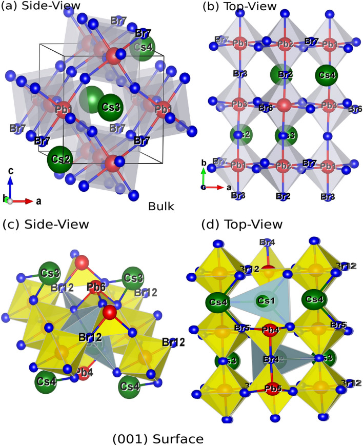
(a, b) Top and Side View of orthorhombic CsPbBr3 and (c, d) Top and Side View of 001-surface of CsPbBr3 along with polyhedra cage (Cs-green, Pb-red, Br-blue).
Result and discussion
The energy-volume curve is obtained by fitting the data obtained from first principles self-consistent force (SCF) calculation in the third order Murnaghan equation of state55 as
| 3 |
The volume optimization curve for both the bulk and the surface is shown in Fig. 2a and b. The atomic positions, previous experimental/theoretical lattice constants45,56 and optimized lattice constants are presented in Table 1. Our calculated lattice constant varies by a very small amount, . The lattice constants of the surface after symmetry operation has become (Å) and (Å) taking the space group P21/m. While after volume optimization, the optimized lattice constants for 001-surface are (Å) and (Å). The bulk modulus (B) is the natural output of volume-optimization. The calculated bulk modulus GPa in good agreement with the previous results 26.841 (LDA)45, 19.203 (GGA)45, 22.759 (PBE-sol)45, 21.5657 and 18 GPa56. We also report the bulk modulus of surface CsPbBr3 9.618 GPa which is almost half of its bulk counterpart.
Figure 2.

Variation of Ground state energy and Volume (V) for (a) Bulk and (b) Surface of CsPbBr (Cs-green, Pb-red, Br-blue).
Table 1.
Atomic positions, experimental lattice constants and theoretical (calculated in this work) lattice constants of orthorhombic bulk CsPbBr3.
| Atom | Expt. position | Expt. lat const. (Å) | Th. lat const. (Å) | ||||||
|---|---|---|---|---|---|---|---|---|---|
| x | y | z | |||||||
| Cs | 0.008 | 0.032 | 0.750 | 8.370 | 12.011 | 8.425a | 8.343 | 11.973 | 8.398 |
| 0.492 | 0.532 | 0.750 | 8.561 | 12.187 | 8.514b | ||||
| 0.508 | 0.468 | 0.250 | |||||||
| 0.992 | 0.968 | 0.250 | |||||||
| Pb | 0.000 | 0.500 | 0.000 | ||||||
| 0.000 | 0.500 | 0.500 | |||||||
| 0.500 | 0.000 | 0.500 | |||||||
| 0.500 | 0.000 | 0.000 | |||||||
| Br | 0.048 | 0.506 | 0.250 | ||||||
| 0.205 | 0.795 | 0.974 | |||||||
| 0.205 | 0.795 | 0.526 | |||||||
| 0.295 | 0.295 | 0.974 | |||||||
| 0.295 | 0.295 | 0.526 | |||||||
| 0.452 | 0.006 | 0.250 | |||||||
| 0.548 | 0.994 | 0.750 | |||||||
| 0.705 | 0.705 | 0.026 | |||||||
| 0.705 | 0.705 | 0.474 | |||||||
| 0.795 | 0.205 | 0.026 | |||||||
| 0.795 | 0.205 | 0.474 | |||||||
| 0.952 | 0.494 | 0.750 | |||||||
Electronic properties
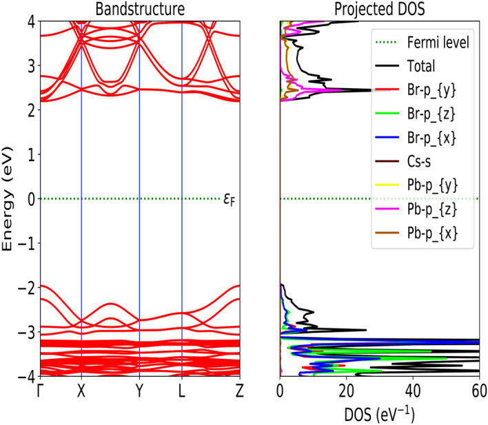
The optimized structure has been used for the calculation of electronic and optical properties of both the bulk and surface structure from DFT-1/2 approach. The importance of DFT-1/2 in predicting accurate electronic bandgap (10 eV) and convergence feasibility has already been discussed. In our study both bulk and surface structure exhibit a semiconducting behaviour with a bandgap of 2.36 eV and 3.82 eV, respectively (see Figs. 3, 4). The presence of Fermi level (E) at the middle of the bandgap indicate its intrinsic behaviour with a direct bandgap along symmetry. Our result of electronic band-gaps calculated from semi-local DFT-1/2 are in consistent with the previous results obtained from higher order DFT functional like GW, HSE, mBJ etc., and experiment [for numerical comparison see Table 2]. Meanwhile, DFT-1/2 open up the the underestimated bandgap from GGA and local density approximation (LDA) by 20%. Our result of bandgap (2.36 eV) for orthorhombic CsPbBr from DFT-1/2 approximation is in consistent with the experimental value of 2.23 eV58, 2.446 eV59 and 2.36 eV60. It also agrees well with the result (2.28 eV) of higher order DFT like HSE0361. Hussain et al., reported the reduced band gap of 1.27 eV, 1.16 eV and 1.08 eV for the cubic, tetragonal and orthorhombic phases, respectively, using spin-orbit coupling in WIEN2K code62. While Yang has reported 1.11 eV for the cubic phase incorporating spin-orbit coupling in VASP package63 From Fig. 3, we have observed that the top of the valence band is mainly composed of Cs-s and Pb-p. It clearly shows the s-state of Cs atom overlap with the state of Pb atom indicating a strong hybridization, while the non-bonding states are formed at the conduction region far above the Fermi level. The Br-p and Pb-p states form a covalent bond. While the Cs-s and Br-p gives a weak ionic bonding. The majority contribution at the bottom of the conduction band merely comes from the Br-p states and empty Pb-p states. The two-fold degenerated bands along the symmetry, infer the presence of heavy and light effective masses of electrons, already discussed elsewhere45. Figure 5a and b, shows the top and side view of 3D electron density plot of bulk orthorhombic CsPbBr. Figure 5c and d, displays the top and side view of 3D electron density plot of 001-surface of CsPbBr. The localization of density is given by yellow sphere around the Pb and Cs atoms.
Figure 3.

Band structure and density of states (DOS) of bulk orthorhombic CsPbBr calculated from DFT-1/2.
Figure 4.
Band structure and density of states (DOS) of 001-surface of CrPbBr calculated from DFT-1/2.
Table 2.
Result of electronic bandgap (E) in eV of bulk and surface of CsPbBr from DFT-1/2 and comparison with the results of other functional.
| Functional | Cubic | Tetragonal | Orthorhombic | Surface |
|---|---|---|---|---|
| DFT-1/2 | – | – | 2.36 | 3.82 |
| PBE-GGA | 1.40a,1.76b,1.6f | 1.49b | 1.78b, 2.00c, 2.29g | 1.78a |
| 2.154d | ||||
| EV-GGA | 2.10b, 1.764e | 1.92b, 2.3d | 2.16b, 2.11g | – |
| PBEsol-GGA | 1.65b, 2.633h | 1.40b, 1.9i | 1.68b, 2.60g | – |
| mBJ-GGA | 2.66b, 2.36d | 2.35b | 2.58b, 3.4g, 2.23d | – |
| mBJ-GGA-SO | 1.81b | 1.69b | 1.82b, 2.73d | – |
| HSE6-SO | 2.74j | – | – | – |
| Expt. | 2.30k | 2.36n | 2.84l/2.3p | |
| 2.36l | 2.24n | 2.93q | ||
| 2.32m | 2.32o |
Figure 5.

(a, b) Top-side view of 3D electron density map of bulk orthorhombic CrPbBr and (c, d) Top-side view of 3D electron density map of 001-surface of CsPbBr.
On the other hand the exfoliation of ultra-thin 001-surface of CsPbBr shows the large opening of band gap by 42% as compared to the bulk. Despite, widening of the band gap of the 001-surface, the electronic band morphology has been preserved with its direct band gap along symmetry. Similar to the bulk, we have noticed a coupling between Pb-Br, and Cs-Br ions, suggesting covalent and ionic bond, respectively, in surface as well (see Fig. 4). Brescia et al.59, formulated an expression for theoretical prediction of onset band gap by fitting a power function with a set of experimentally determined bandgap as a function of film thickness in relation to effective mass .
| 4 |
where and are the energy band gap of bulk and film of thickness (t) respectively. It is obvious from the above expression that the decrease in film thickness will increase the energy band gap of the thin film. In Fig. 6, we have presented the variation of energy bandgap as a funtion of slab thickness of CsPbBr. The curve is fitted based on the Eq. (4) using gnuplot. The similar trend of increase in band gap from 2.47 eV to 2.84 eV on decreasing the slab from 151 layer has also been reported from PWscf PBE-SOC (spin-orbit coupling) calculation70.
Figure 6.
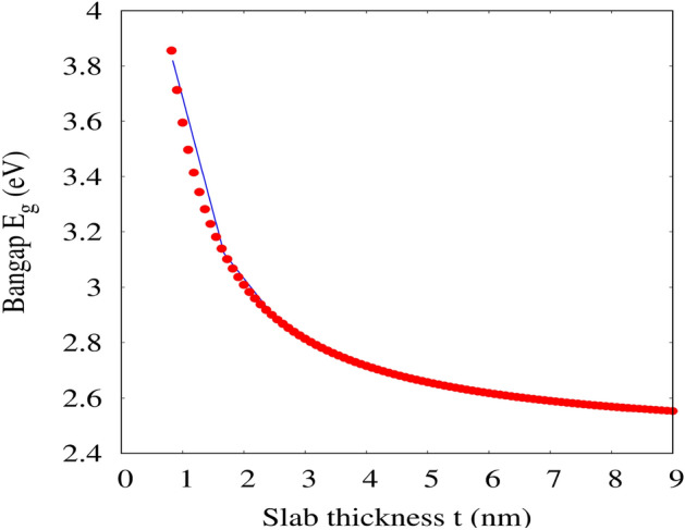
The variation of energy bandgap (E) as a function of slab thickness (t) of 001-surface of CrPbBr using DFT-1/2 (blue line represent the results of energy bandgap and red dot denotes the data fit using Eq. (4) from gnuplot).
The increased in the direct band gap of the surface state may be infer to quantum confinement effect74. The halide based nanoparticles perovskite exhibit quantum confinement effect for a nanometer-size (< 50 nm) and strong Mie resonances above 102 nm75. We have arbitrarily determine the electron effective mass of 001-surface using Eq. (4), taking the single layer thickness Å, eV and eV. The estimated electron effective mass of 001-surface is found to be 0.20, in good agreement with 0.24 (single slab) and 0.17 (bulk)70.
Optical properties
For better explanation of the optical response the electron transitions are considered from the first three valence bands below E to first three conduction bands above the E. The probability transition along the various symmetry points in the first Brillouin zone and their corresponding maximum energies give the information about the optical properties. The optical response with respect to the incident photon energy is presented in the form of a complex dielectric function given by;
| 5 |
Here and are real and imaginary parts of the dielectric function respectively. The imaginary part can be calculated using Eq. (2),
| 6 |
where - momentum operator, - eigen-function of eigenvalue, f()-Fermi Distribution function. The Kramers–Kronig transformation helps in finding the real part of the dielectric function from its corresponding imaginary part as :
| 7 |
The absorption coefficients , which is related to the dielectric function is given as follows;
| 8 |
The real part of refractive index (n) is given by
| 9 |
The optical parameters of both bulk and surface like real part of dielectric function (), imaginary part of dielectric function(), absorption coefficient(, reflectivity() and refractive index () are presented in Figs. 7, 8 and 9. In all figures we have used black, red and green color lines to represent the polarization along x, y and z-axes, respectively. Fig.7a and b represent the real and imaginary part of dielectric function for the bulk system. The rises slowly and reach maximum at 2.35 eV, in which the dielectric polarization along z-axis predominate. After 2.5 eV the decreases sharply and drops below 0 at 3.0 eV. The drop of below zero gives negative value in which the incident photon beam is attenuated due to the dissipation of energy into the medium and giving rise to metallic behaviour. The drop of from maximum value can be relate to the rise of , suggesting inter-band transition. The intensity of increases slowly after 3.0 eV and gives a constant intensity of 1.0 for all values of photon energy above 5.0 eV. The static value of real dielectric constant [] is inversely related to the energy bandgap by;
| 10 |
Figure 7.

(a) Real part of dielectric function () of bulk (b) Imaginary part of dielectric function () of bulk, (c) Real part of dielectric function () of 001-surface (d) Imaginary part of dielectric function () of 001-surface, [*our result is compared with the experimental spectra of and (denoted by red dot) Expt.76].
Figure 8.

Absorption coefficient () of bulk with respect to (a) Photon energy (eV) (b) Wavelength (nm), and Absorption coefficient () of 001-surface with respect to (c) Photon energy (eV) (d) Wavelength (nm).
Figure 9.

(a) Reflectivity (r) of bulk, (b) Refractive index (n) of bulk, (c)Reflectivity (r) of 001-surface, (d) Refractive index (n) of 001-surface.
From the above Eq. (10), the higher value of bandgap leads to the low value of . It is well verified that the higher value of bandgap (3.82 eV) in the surface system gives far lower value of =1.10, as compared to the bulk system [=1.72]. The calculated values of along the different polarization direction is tabulated in Table 3. In spectra the maximum peak occurs at around 3.45 eV (see Fig. 7b). We have presented the spectra of 001 surface of CsPbBr obtained from DFT-1/2 in Fig.7d. Unfortunately, we did not find any experimental result of spectra of the thin film of CsPbBr for direct comparision. Therefore, the calculated is compared with the available result of nanocrystalline orthorhombic CsPbBr calculated at different temperatures from high-resolution spectroscopic ellipsometry, high-resolution transmission electron microscopy and terahertz spectroscopy measurements76. The theoretical calculated from DFT-1/2 and experimental76 are plotted together in Fig. 7d for better comparision. Here, along x and y-axes predominates, due to the 2D nature of CsPbBr. The maximum value of occurs at 4.20 eV. It seems that the maximum peak of spectra has shifted towards the higher energy as compared to its bulk counter part. The highest peak of is located at 4.60 eV.
Table 3.
Static real part of dielectric function and static refractive index n(0) of orthorhombic bulk and surface of CsPbBr.
| Structure | n(0) | |||||
|---|---|---|---|---|---|---|
| Bulk | 1.720 | 1.720 | 1.800 | 1.300 | 1.300 | 1.320 |
| Surface | 1.100 | 1.100 | 1.060 | 1.045 | 1.045 | 1.040 |
The absorption coefficient () for both the bulk and the surface with respect to the photon energy and the wavelength is displayed in Fig. 8a–d. The positive tangent drawn on the cut the x-axis somewhere at 2.30 eV, which may be considered as an optical band gap (Fig. 8a). From, Fig. 8b, the estimated absorption onset is 540 nm, which is in good agreement with 554 nm58. Majhi et al., prepared the orthorhombic CsPbBr from wet chemical synthesis method and studied the optoelectronic properties by UV–Vis and photoluminescence (PL) spectroscopy in which they reported the band-to-band transition at 554 nm (2.23 eV)58, which may be considered as an optical band gap. This spectra can be related to the first electron transition from top of the valence band to the bottom of conduction band along direction. For the bulk system an absorption peak of magnitude 4.510 cm appears at 4.0 eV, has zero absorption intensity in the range of 0–2 eV and beyond 6.0 eV (see Fig. 8a). This proves that the for the bulk CsPbBr the energy active window lies between 2.3 and 5.0 eV, having width of 2.70 eV. We have observed a reduce absorption peak in the case of surface system. The intensity of the peak for the surface is 1.5810 cm at 5.60 eV (see Fig.8c). The magnitude of = 1.5810 cm comprehended well with the experimental result77. The energy active window found in between 4 and 6.5 eV, giving rise to the window width of 2.5 eV. The window width for the bulk system is little high as compared to the surface by =0.20 eV. The absorption onset is found at 340 nm (see Fig.8d). There is a shift in the absorption peak by 1.60 eV towards the higher energy while scaling from the infinite layers (bulk) to a single layer (surface). We have observed a prominent feature of a blue-shift in diminishing a structure size from bulk to surface(ultra thin film). It has already been shown that the perovskite with the slab thickness below 3.0 nm exhibit a blue shift [see Fig. 3 of Ref.70]. Most of the MAPbBr perovskite nanoparticles of larger sizes (more than 50–100 nm) exhibit the influence of enhanced Mie modes preserving the blue shift despite the of feeble quantum confinement effect75. Electron energy-loss spectroscopy (EELS) reported the onset optical gap of around 2.4–2.5 eV for a 10 nm thick thin film of CsPbBr59. The thin film of CsPbBr perovskite prepared from Single Source Thermal Ablation shows absorption onset at 530 nm78. Also, the CsPbBr film prepared by 2-step sequential deposition, exhibit prominent absorbance peaks at 510–525 nm, with absorbance onset at 532 nm79.
We have presented the calculated spectra of reflectivity and the refractive index for both the bulk and surface systems in Fig. 9a–d. At the initial part of the photon energy, the reflectivity spectra is very low and increases with the increase in the energy and ultimately give maximum reflectivity of 35.0% at 4.0 eV (see Fig. 9a). Meanwhile, the maximum reflectivity of the surface is only 2.0%, this may be due to its transparent behaviour within UV–Vis range of the electro-magnetic radiation Fig. 9c. The maximum surface reflectivity occurs at 5.60 eV. Fig. 9b and d, shows the refractive index of the bulk and the surface. The static refractive indices for the bulk system along x and z-direction are 1.72 and 1.80, respectively. This result is in good agreement with the previous result of 1.9645,46. From the static value, the increases to reach the maximum value at 3.20 eV. Beyond 3.20 eV the spectra of decreases rapidly and goes below 1.0 at 3.40 eV in the UV-region. If we refer to Fig. 7a, we can see the value of becomes negative at this value of energy (3.40 eV). The presence of value below 1.0 is nonphysical in which the phase velocity move faster than the group velocity (speed of light). This can be related to the occurrence of the plasmonic vibration with the plasmonic frequency () close to resonance frequency. The static refractive index of the surface is found to be n(0)=1.045 which is close to 1.0, indicating transparent behaviour within visible range of light. In case of the surface the plasmonic vibration lies at 5.2 eV.
Conclusions
For the first time, we have carried out the electronic and optical properties of the orthorhombic bulk and 001-surface of CsPbBr from DFT-1/2 approach. This work also performed to test the efficiency of DFT-1/2 in deriving the electronic and optical properties of inorganic perovskite. Herein, we report the efficiency of DFT-1/2 is as effective as that of higher order DFT like HSE hybrid functional in calculating the electronic bandgap. The calculated band gap is 2.36 eV in good agreement with the experiment. While, the ultra-thin surface slab of CsPbBr open up the electronic bandgap by 42%. We report the decrease in bandgap while increasing the slab thickness of CsPbBr film. The thin film of CsPbBr exhibit tunability of the bandgap via the surface thickness modification. The presence of high value of absorption coefficient 4.510 cm and 1.5810 cm in UV–Vis energy range for both the bulk and the surface, respectively. The tunability of energy bandgap offers remarkable optoelectronic properties in UV–Vis range making this material promising for optoelectronic applications.
Acknowledgements
The authors extend their appreciation to the Deanship of Scientific Research at Jouf University for funding this work through research grant no. (DSR-2021-03-0219).
Author contributions
M.E., T.V.V. and D.P.R. supervised and drafted this project. M.E., D.P.R., and T.V.V. performed the structural, electronic and optical calculations. S.A.Q., Z.A.A., M.A., E.M., and A.E.S. visualized, analyzed and concenptualized the results. All authors contributed in review and revised this manuscript.
Data availability
The data for this paper are available from D.P.R (dibya@pucollege.edu.in) & M.E (Meabas@ju.edu.sa).
Competing interests
The authors declare no competing interests.
Footnotes
Publisher's note
Springer Nature remains neutral with regard to jurisdictional claims in published maps and institutional affiliations.
These authors contributed equally: Mohammed Ezzeldien and Tuan V. Vu.
References
- 1.Yi Z, et al. Will organic-inorganic hybrid halide lead perovskites be eliminated from optoelectronic applications? Nanosc. Adv. 2019;1:1276–1289. doi: 10.1039/C8NA00416A. [DOI] [PMC free article] [PubMed] [Google Scholar]
- 2.Chen Q, et al. Under the spotlight: The organic-inorganic hybrid halide perovskite for optoelectronic applications. Nano Today. 2015;10:355–396. doi: 10.1016/j.nantod.2015.04.009. [DOI] [Google Scholar]
- 3.Ouyang Y, et al. Photo-oxidative degradation of methylammonium lead iodide perovskite: Mechanism and protection. J. Mater. Chem. A. 2019;7:2275–2282. doi: 10.1039/C8TA12193A. [DOI] [Google Scholar]
- 4.Wang B, et al. Efficient charge separation and visible-light response in bilayer HfS 2 -based van der Waals heterostructures. RSC Adv. 2018;8:18889–18895. doi: 10.1039/C8RA03047B. [DOI] [PMC free article] [PubMed] [Google Scholar]
- 5.Zhao X, et al. Efficient planar perovskite solar cells with improved fill factor via interface engineering with graphene. Nano Lett. 2018 doi: 10.1021/acs.nanolett.8b00025. [DOI] [PubMed] [Google Scholar]
- 6.Pitriana P, Wungu TDK, Hidayat R. The characteristics of band structures and crystal binding in all-inorganic perovskite APbBr3 studied by the first principle calculations using the Density Functional Theory (DFT) method. Results Phys. 2019;15:102592. doi: 10.1016/j.rinp.2019.102592. [DOI] [Google Scholar]
- 7.Yin WJ, Yang JH, Kang J, Yan Y, Wei SH. Halide perovskite materials for solar cells: A theoretical review. J. Mater. Chem. A. 2015 doi: 10.1039/c4ta05033a. [DOI] [Google Scholar]
- 8.Huang Y, Sun QD, Xu W, He Y, Yin WJ. Halide perovskite materials for solar cells: A theoretical review. J. Mater. Chem. A. 2017 doi: 10.3866/PKU.WHXB201705042. [DOI] [Google Scholar]
- 9.Mao X, et al. First-principles screening of all-inorganic lead-free ABX 3 perovskites. J. Phys. Chem. C. 2018;122:7670–7675. doi: 10.1021/acs.jpcc.8b02448. [DOI] [Google Scholar]
- 10.Stranks SD, et al. Electron–hole diffusion lengths exceeding 1 micrometer in an organometal trihalide perovskite absorber. Science. 2013;342:341–344. doi: 10.1126/science.1243982. [DOI] [PubMed] [Google Scholar]
- 11.Green MA, Ho-Baillie A, Snaith HJ. The emergence of perovskite solar cells. Nat. Photon. 2014;8:506–514. doi: 10.1038/nphoton.2014.134. [DOI] [Google Scholar]
- 12.Ling Y, et al. Bright light-emitting diodes based on organometal halide perovskite nanoplatelets. Adv. Mater. 2016;28:305–311. doi: 10.1002/adma.201503954. [DOI] [PubMed] [Google Scholar]
- 13.Dong H, Zhang C, Liu X, Yao J, Zhao YS. Materials chemistry and engineering in metal halide perovskite lasers. Chem. Soc. Rev. 2020;49:951–982. doi: 10.1039/C9CS00598F. [DOI] [PubMed] [Google Scholar]
- 14.Liao Q, Jin X, Fu H. Tunable halide perovskites for miniaturized solid-state laser applications. Adv. Opti. Mater. 2019;7:1900099. doi: 10.1002/adom.201900099. [DOI] [Google Scholar]
- 15.Xu P. All-inorganic perovskite CsPbI2Br as a promising photovoltaic absorber: A first-principles study. J. Chem. Sci. 2020 doi: 10.1007/s12039-020-01780-7. [DOI] [Google Scholar]
- 16.Noh JH, Im SH, Heo JH, Mandal TN, Seok SI. Chemical management for colorful, efficient, and stable inorganic-organic hybrid nanostructured solar cells. Nano Lett. 2013;13:1764–1769. doi: 10.1021/nl400349b. [DOI] [PubMed] [Google Scholar]
- 17.Hao F, Stoumpos CC, Chang RPH, Kanatzidis MG. Anomalous band gap behavior in mixed Sn and Pb perovskites enables broadening of absorption spectrum in solar cells. J. Am. Chem. Soc. 2014;136:8094–8099. doi: 10.1021/ja5033259. [DOI] [PubMed] [Google Scholar]
- 18.Ahmad K, et al. Instability in CH3NH3PbI3 perovskite solar cells due to elemental migration and chemical composition changes. Sci. Rep. 2017;7:15406. doi: 10.1038/s41598-017-15841-4. [DOI] [PMC free article] [PubMed] [Google Scholar]
- 19.Liu D, Zha W, Guo Y, Sa R. Insight into the improved phase stability of CsPbI3 from first-principles calculations. ACS Omega. 2020;5:893–896. doi: 10.1021/acsomega.9b03838. [DOI] [PMC free article] [PubMed] [Google Scholar]
- 20.Hoefler SF, Trimmel G, Rath T. Progress on lead-free metal halide perovskites for photovoltaic applications: A review. Monatsh. Chem. Chem. Mon. 2017;148:795–826. doi: 10.1007/s00706-017-1933-9. [DOI] [PMC free article] [PubMed] [Google Scholar]
- 21.Bala A, Kumar V. Stability of the Eu2+ dopant in CsPbBr3 perovskites: A first-principles study. J. Phys. Chem. C. 2019;123:6965–6969. doi: 10.1021/acs.jpcc.8b10261. [DOI] [Google Scholar]
- 22.Liang J, et al. CsPb0.9Sn0.1IBr2 based all-inorganic perovskite solar cells with exceptional efficiency and stability. J. Am. Chem. Soc. 2017;139:14009–14012. doi: 10.1021/jacs.7b07949. [DOI] [PubMed] [Google Scholar]
- 23.Leijtens T, et al. Stability of metal halide perovskite solar cells. Adv. Energy Mater. 2015;5:1500963. doi: 10.1002/aenm.201500963. [DOI] [Google Scholar]
- 24.Zhang X, Zhou F, Zhang S, Liang Y, Wang R. Engineering MoS 2 basal planes for hydrogen evolution via synergistic ruthenium doping and nanocarbon hybridization. Adv. Sci. 2019;6:1900090. doi: 10.1002/advs.201900090. [DOI] [PMC free article] [PubMed] [Google Scholar]
- 25.Zhou Y, Zhao Y. Chemical stability and instability of inorganic halide perovskites. Energy Environ. Sci. 2019;12:1495–1511. doi: 10.1039/C8EE03559H. [DOI] [Google Scholar]
- 26.McGrath F, Ghorpade UV, Ryan KM. Synthesis and dimensional control of CsPbBr3 perovskite nanocrystals using phosphorous based ligands. J. Chem. Phys. 2020 doi: 10.1063/1.5128233. [DOI] [PubMed] [Google Scholar]
- 27.Beal RE, et al. Cesium lead halide perovskites with improved stability for tandem solar cells. J. Phys. Chem. Lett. 2016;7:746–751. doi: 10.1021/acs.jpclett.6b00002. [DOI] [PubMed] [Google Scholar]
- 28.Ouedraogo NAN, et al. Stability of all-inorganic perovskite solar cells. Nano Energy. 2020 doi: 10.1016/j.nanoen.2019.104249. [DOI] [Google Scholar]
- 29.Wang B, Navrotsky A. Thermodynamics of cesium lead halide (CsPbX3, x= I, Br, Cl) perovskites. Thermochim. Acta. 2021 doi: 10.1016/j.tca.2020.178813. [DOI] [Google Scholar]
- 30.Nedelcu G, et al. Fast anion-exchange in highly luminescent nanocrystals of cesium lead halide perovskites (CsPbX 3, X = Cl, Br, I) Nano Lett. 2015;15:5635–5640. doi: 10.1021/acs.nanolett.5b02404. [DOI] [PMC free article] [PubMed] [Google Scholar]
- 31.Liashenko TG, et al. Electronic structure of CsPbBr3-xClx perovskites: Synthesis, experimental characterization, and DFT simulations. Phys. Chem. Chem. Phys. 2019;21:18930–18938. doi: 10.1039/c9cp03656c. [DOI] [PubMed] [Google Scholar]
- 32.Zhang X, et al. All-ambient processed binary CsPbBr3 -CsPb 2 Br 5 perovskites with synergistic enhancement for high-efficiency Cs-Pb-Br-based solar cells. ACS Appl. Mater. Interfaces. 2018;10:7145–7154. doi: 10.1021/acsami.7b18902. [DOI] [PubMed] [Google Scholar]
- 33.Ahmad M, et al. Structural, electronic and optical properties of CsPbX3 (X=Cl, Br, I) for energy storage and hybrid solar cell applications. J. Alloys Compd. 2017;705:828–839. doi: 10.1016/j.jallcom.2017.02.147. [DOI] [Google Scholar]
- 34.Jong U-G, et al. A first-principles study on the chemical stability of inorganic perovskite solid solutions Cs 1x Rb x PbI 3 at finite temperature and pressure. J. Mater. Chem. A. 2018;6:17994–18002. doi: 10.1039/C8TA06553E. [DOI] [Google Scholar]
- 35.He Y, et al. High spectral resolution of gamma-rays at room temperature by perovskite CsPbBr3 single crystals. Nat. Commun. 2018;9:1609. doi: 10.1038/s41467-018-04073-3. [DOI] [PMC free article] [PubMed] [Google Scholar]
- 36.dos Reis R, et al. Determination of the structural phase and octahedral rotation angle in halide perovskites. Appl. Phys. Lett. 2018;112:071901. doi: 10.1063/1.5017537. [DOI] [Google Scholar]
- 37.Luther JM, et al. Quantum dot-induced phase stabilization ofa-CsPbI3 perovskite for high-efficiency photovoltaics. Science. 2016;354:1–10. doi: 10.1126/science.aag2700. [DOI] [PubMed] [Google Scholar]
- 38.Yang C, Wang HF, Xu Q. Recent advances in two-dimensional materials for electrochemical energy storage and conversion. Science. 2020 doi: 10.1007/s40242-020-9068-7. [DOI] [Google Scholar]
- 39.Dong X, et al. Trivalent ion mediated abnormal growth of all-inorganic perovskite nanocrystals and their divergent emission properties. Nanoscale. 2019 doi: 10.1039/c9nr01764j. [DOI] [PubMed] [Google Scholar]
- 40.Ma S, et al. Strain-mediated phase stabilization: A new strategy for ultrastable -CsPbI3 perovskite by nanoconfined growth. Small. 2019 doi: 10.1002/smll.201900219. [DOI] [PubMed] [Google Scholar]
- 41.Oksenberg E, Sanders E, Popovitz-Biro R, Houben L, Joselevich E. Surface-guided CsPbBr3 perovskite nanowires on flat and faceted sapphire with size-dependent photoluminescence and fast photoconductive response. Nano Lett. 2018 doi: 10.1021/acs.nanolett.7b04310. [DOI] [PubMed] [Google Scholar]
- 42.Yu Z, Wan N, Lei S, Yu H. Enhanced hydrogen storage by using lithium decoration on phosphorene. J. Appl. Phys. 2016;120:024305. doi: 10.1063/1.4958695. [DOI] [Google Scholar]
- 43.Yang Y, Hou C, Liang TX. Energetic and electronic properties of CsPbBr3 surfaces: A first-principles study. Phys. Chem. Chem. Phys. 2021;23:7145–7152. doi: 10.1039/d0cp04893c. [DOI] [PubMed] [Google Scholar]
- 44.Kohn W, Sham LJ. Self-consistent equations including exchange and correlation effects. Phys. Rev. 1965;140:A1133–A1138. doi: 10.1103/PhysRev.140.A1133. [DOI] [Google Scholar]
- 45.Ghaithan HM, Alahmed ZA, Qaid SM, Aldwayyan AS. Structural, electronic, and optical properties of cspb(Br 1xclx)3 perovskite: First-principles study with pbe-gga and mbj-gga methods. Materials. 2020;13:4944. doi: 10.3390/ma13214944. [DOI] [PMC free article] [PubMed] [Google Scholar]
- 46.Ghaithan HM, Alahmed ZA, Qaid SM, Hezam M, Aldwayyan AS. Density functional study of cubic, tetragonal, and orthorhombic CsPbBr3 perovskite. ACS Omega. 2020;5:7468–7480. doi: 10.1021/acsomega.0c00197. [DOI] [PMC free article] [PubMed] [Google Scholar]
- 47.Smidstrup S, et al. QuantumATK: An integrated platform of electronic and atomic-scale modelling tools. J. Phys. Condens. Matter. 2020;32:015901. doi: 10.1088/1361-648X/ab4007. [DOI] [PubMed] [Google Scholar]
- 48.Smidstrup S, et al. First-principles Green’s-function method for surface calculations: A pseudopotential localized basis set approach. Phys. Rev. B. 2017;96:195309. doi: 10.1103/PhysRevB.96.195309. [DOI] [Google Scholar]
- 49.Ferreira LG, Marques M, Teles LK. Approximation to density functional theory for the calculation of band gaps of semiconductors. Phys. Rev. B. 2008;78:125116. doi: 10.1103/PhysRevB.78.125116. [DOI] [Google Scholar]
- 50.Ferreira LG, Marques M, Teles LK. Slater half-occupation technique revisited: the LDA-1/2 and GGA-1/2 approaches for atomic ionization energies and band gaps in semiconductors. AIP Adv. 2011;1:032119. doi: 10.1063/1.3624562. [DOI] [Google Scholar]
- 51.Tao SX, Cao X, Bobbert PA. Accurate and efficient band gap predictions of metal halide perovskites using the DFT-1/2 method: GW accuracy with DFT expense. Sci. Rep. 2017;7:14386. doi: 10.1038/s41598-017-14435-4. [DOI] [PMC free article] [PubMed] [Google Scholar]
- 52.Rai DP, Singh YT, Chettri B, Houmad M, Patra PK. A theoretical investigation of electronic and optical properties of (6,1) single-wall carbon nanotube (SWCNT) Carbon Lett. 2020 doi: 10.1007/s42823-020-00172-8. [DOI] [Google Scholar]
- 53.Rai D, et al. Electronic, magnetic and optical properties of monolayer (ML) hexagonal ZnSe on vacancy defects at Zn sites from DFT-1/2 approach. Vacuum. 2020;182:109597. doi: 10.1016/j.vacuum.2020.109597. [DOI] [Google Scholar]
- 54.Perdew JP, Burke K, Ernzerhof M. Perdew, Burke, Ernzerhof: Generalized gradient approximation made simple. Phys. Rev. Lett. 1996;77:3865–3868. doi: 10.1103/PhysRevLett.77.3865. [DOI] [PubMed] [Google Scholar]
- 55.Murnaghan FD. The compressibility of media under extreme pressures. Proc. Natl. Acad. Sci. 1944;30:244–247. doi: 10.1073/pnas.30.9.244. [DOI] [PMC free article] [PubMed] [Google Scholar]
- 56.Project, T. M. Materials data on CsPbBr3 by materials project. 10.17188/1273967 (2017).
- 57.Welch EW, Jung YK, Walsh A, Scolfaro L, Zakhidov A. A density functional theory study on the interface stability between CsPbBr3 and CuI. AIP Adv. 2020 doi: 10.1063/5.0018925. [DOI] [Google Scholar]
- 58.Maji P, Sadhukhan P, Das S. Optoelectronic properties of facile synthesized orthorhombic cesium lead bromide (CsPbBr3) J. Mater. Sci. 2020 doi: 10.1007/s10854-020-04270-1. [DOI] [Google Scholar]
- 59.Brescia R, et al. Bandgap determination from individual orthorhombic thin cesium lead bromide nanosheets by electron energy-loss spectroscopy. Nanosc. Horizons. 2020 doi: 10.1039/d0nh00477d. [DOI] [PubMed] [Google Scholar]
- 60.Paul T, et al. Tunable cathodoluminescence over the entire visible window from all-inorganic perovskite CsPbX3 1D architecture. J. Mater. Chem. C. 2018 doi: 10.1039/c7tc05703b. [DOI] [Google Scholar]
- 61.Cen G, et al. Precise phase control of large-scale inorganic perovskites via vapor-phase anion-exchange strategy. Small. 2020 doi: 10.1002/smll.202005226. [DOI] [PubMed] [Google Scholar]
- 62.Hussain M, Rashid M, Saeed F, Bhatti A. Spin-orbit coupling effect on energy level splitting and band structure inversion in CsPbBr. J. Mater. Sci. 2020;56:1–15. doi: 10.1007/s10853-020-05298-8. [DOI] [Google Scholar]
- 63.Yang K, Setyawan W, Wang S, Nardelli MB, Curtarolo S. A search model for topological insulators with high-throughput robustness descriptors. Nat. Mater. 2012;11:614–619. doi: 10.1038/NMAT3332. [DOI] [PubMed] [Google Scholar]
- 64.Verma AS, Kumar A, Bhardwaj SR. Correlation between ionic charge and the lattice constant of cubic perovskite solids. Phys. Status Solidi B. 2008 doi: 10.1002/pssb.200844072. [DOI] [Google Scholar]
- 65.Murtaza G, Ahmad I. First principle study of the structural and optoelectronic properties of cubic perovskites CsPbM3 (M=Cl, Br, I) Physica B. 2011 doi: 10.1016/j.physb.2011.05.028. [DOI] [Google Scholar]
- 66.Kang B, Biswas K. Exploring polaronic, excitonic structures and luminescence in Cs4PbBr6/CsPbBr3. J. Phys. Chem. Lett. 2018 doi: 10.1021/acs.jpclett.7b03333. [DOI] [PubMed] [Google Scholar]
- 67.Ye Y, et al. Nature of the band gap of halide perovskites ABX3 (A= CH3NH3, Cs; B= Sn, Pb; X= Cl, Br, I): First-principles calculations. Chin. Phys. B. 2015;24:1–10. [Google Scholar]
- 68.Castelli IE, García-Lastra JM, Thygesen KS, Jacobsen KW. Bandgap calculations and trends of organometal halide perovskites. APL Mater. 2014 doi: 10.1063/1.4893495. [DOI] [Google Scholar]
- 69.Heidrich K, et al. Electronic structure, photoemission spectra, and vacuum-ultraviolet optical spectra of CsPbCl3 and CsPbBr3. Phys. Rev. B. 1981;24:5642–5649. doi: 10.1103/PhysRevB.24.5642. [DOI] [Google Scholar]
- 70.Akkerman QA, et al. Solution synthesis approach to colloidal cesium lead halide perovskite nanoplatelets with monolayer-level thickness control. J. Am. Chem. Soc. 2016;138:1010–1016. doi: 10.1021/jacs.5b12124. [DOI] [PMC free article] [PubMed] [Google Scholar]
- 71.Li Y, et al. Lattice modulation of alkali metal cations doped Cs1xRxPbBr 3 halides for inorganic perovskite solar cells. Solar RRL. 2018;2:1800164. doi: 10.1002/solr.201800164. [DOI] [Google Scholar]
- 72.Zhang Y, Cheng X. Hydrogen storage on Li coated BC 3 honeycomb sheet. Chin. J. Chem. 2017;35:1329–1332. doi: 10.1002/cjoc.201600911. [DOI] [Google Scholar]
- 73.Yan H, Wei Z, Zhang M, Wei Q. Exploration of stable stoichiometries, ground-state structures, and mechanical properties of the W-Si system. Ceram. Int. 2020;46:17034–17043. doi: 10.1016/j.ceramint.2020.03.290. [DOI] [Google Scholar]
- 74.Wang Q, et al. Quantum confinement effect and exciton binding energy of layered perovskite nanoplatelets. AIP Adv. 2018 doi: 10.1063/1.5020836. [DOI] [Google Scholar]
- 75.Berestennikov AS, et al. Beyond quantum confinement: Excitonic nonlocality in halide perovskite nanoparticles with Mie resonances. Nanoscale. 2019;11:6747–6754. doi: 10.1039/c8nr09837a. [DOI] [PubMed] [Google Scholar]
- 76.Whitcher TJ, et al. Dual phases of crystalline and electronic structures in the nanocrystalline perovskite CsPbBr3. NPG Asia Mater. 2019 doi: 10.1038/s41427-019-0170-6. [DOI] [Google Scholar]
- 77.Qaid SM, Ghaithan HM, Al-Asbahi BA, Alqasem A, Aldwayyan AS. Fabrication of thin films from powdered cesium lead bromide (CsPbBr3) perovskite quantum dots for coherent green light emission. ACS Omega. 2020 doi: 10.1021/acsomega.0c04517. [DOI] [PMC free article] [PubMed] [Google Scholar]
- 78.Nasi L, et al. All-inorganic CsPbBr3 perovskite films prepared by single source thermal ablation. Chemistry. 2020 doi: 10.3389/fchem.2020.00313. [DOI] [PMC free article] [PubMed] [Google Scholar]
- 79.Liu D, et al. Two-step method for preparing all-inorganic CsPbBr3 perovskite film and its photoelectric detection application. Mater. Lett. 2017;186:243–246. doi: 10.1016/j.matlet.2016.10.015. [DOI] [Google Scholar]
Associated Data
This section collects any data citations, data availability statements, or supplementary materials included in this article.
Data Availability Statement
The data for this paper are available from D.P.R (dibya@pucollege.edu.in) & M.E (Meabas@ju.edu.sa).