

Abstract

Phosphorus oxide (POx) capped by aluminum oxide (Al2O3) has recently been discovered to provide excellent surface passivation of crystalline silicon (c-Si). In this work, insights into the passivation mechanism of POx/Al2O3 stacks are gained through a systematic study of the influence of deposition temperature (Tdep = 100–300 °C) and annealing temperature (Tann = 200–500 °C) on the material and interface properties. It is found that employing lower deposition temperatures enables an improved passivation quality after annealing. Bulk composition, density, and optical properties vary only slightly with deposition temperature, but bonding configurations are found to be sensitive to temperature and correlated with the interface defect density (Dit), which is reduced at lower deposition temperature. The fixed charge density (Qf) is in the range of + (3–9) × 1012 cm–2 and is not significantly altered by annealing, which indicates that the positively charged entities are generated during deposition. In contrast, Dit decreases by 3 orders of magnitude (∼1013 to ∼1010 eV–1 cm–2) upon annealing. This excellent chemical passivation is found to be related to surface passivation provided by hydrogen, and mixing of aluminum into the POx layer, leading to the formation of AlPO4 upon annealing.
Keywords: silicon, surface passivation, phosphorus oxide, aluminum oxide, interface properties
Introduction
Passivation of crystalline silicon (c-Si) surfaces is important for various (opto)electronic applications, such as photovoltaics,1−5 photonics,6−8 and nanoelectronics,9−11 to avoid recombination losses that would otherwise compromise the device’s performance. This recombination occurs mainly via defect states in the bandgap, which arise predominantly from silicon dangling bonds at the surface.3 Passivation layers, such as SiOx, SiNx, and Al2O3, can be used to suppress the recombination at the silicon surfaces by terminating the Si dangling bonds and thereby lowering the defect concentration, which is known as chemical passivation. Additionally, fixed charges present in the passivation layer or at the interface between the c-Si and the passivation layer can induce band bending in the silicon. This band bending can repel charge carriers and thereby reduce recombination, which is known as field-effect passivation.12 Excellent passivation of c-Si surfaces can be achieved by a proper combination of chemical and field-effect passivation.
In Figure 1, an overview of c-Si surface passivation schemes is shown in terms of interface defect density (Dit) and fixed charge density (Qf), which are generally used as a measure for chemical and field-effect passivation, respectively. This figure is divided into materials with negative (left) and positive fixed charge density (right) on c-Si. The various passivation schemes span a wide range of Dit and Qf values. A low Dit is always favored to obtain good chemical passivation, while a high Qf is desired to obtain good field-effect passivation. The sign of Qf has to be chosen appropriately (ideally negative for p-type Si and positive for n-type Si surfaces) to avoid an increase in minority carrier concentration at the surface, which can lead to additional recombination losses.
Figure 1.
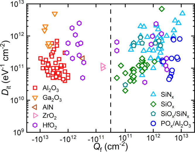
An overview of c-Si surface passivation materials and stacks in terms of interface defect density (Dit) and fixed charge density (Qf). Dit with corresponding Qf are given for Al2O3,15,16,20−26 POx/Al2O3,19 SiNx,27−32 SiOx,33−35 SiOx/SiNx,36,37 Ga2O3,38,39 AlN,40 ZrO2,41 and HfO2.42−45 The data are divided into materials with negative (left) and positive (right) fixed charge on silicon. Other passivating materials, which are not shown because the magnitudes of Dit or Qf have not been reported in the literature, include: Ta2O5 (negative Qf), TiO2 (negative Qf), Nb2O5 (negative Qf), and a-Si:H (very low Dit).
A general trend that appears in Figure 1 is that an increase in magnitude of Qf comes at the expense of an increase in Dit. It is possible that this trend results from defects capturing charge, causing the formation of charged entities. Such an effect has been shown for SiNx, where Si dangling bonds present in the SiNx are able to capture electrons and holes, leading to charged defects.13,14 However, some materials seem to be less prone to this effect than others. Al2O315,16 (red squares) for example can reach a combination of low Dit and high negative Qf, which makes Al2O3 the preferred material for the passivation of p-type silicon surfaces. POx/Al2O317−19 (blue circles) can reach a combination of low Dit and high positive fixed charge (data from the current work also plotted in Figure 1). It therefore appears to be the positively charged counterpart to Al2O3 for c-Si surface passivation, which makes it highly suited for passivating n-type silicon surfaces.
The promise of POx/Al2O3 as a passivation scheme for c-Si surfaces can be clearly seen from Figure 1 and recently several publications on this passivation scheme have appeared. POx/Al2O3 deposited by atomic layer deposition (ALD) was initially reported as a well-suited passivation scheme for InP nanowires46 and it has been found that it can also provide excellent passivation of c-Si surfaces.18 The passivation quality on n-type as well as p-type Si surfaces was investigated along with the effect of the POx thickness, annealing temperature, and annealing time.17 It has been shown that self-aligned contact openings with local n+ doping can be achieved from the POx/Al2O3 stack using nanosecond laser pulses.47 The passivation on textured Si and n+-doped Si surfaces was studied using a pulsed-flow plasma-enhanced chemical vapor deposition process.19 These investigations have been very useful to show the potential of POx/Al2O3 stacks as a versatile passivation scheme. However, the passivation mechanism of POx/Al2O3 is not well understood yet, and systematic studies of the material and interface properties are still lacking.
In this work, we have investigated films prepared at various deposition temperatures to study the material and interface properties of the POx/Al2O3 stack, which relate to the passivation quality. We have investigated structural and compositional changes of POx/Al2O3 stacks due to postdeposition annealing, as well as the effusion of hydrogen from the stack upon annealing. From the results, an improved understanding of the POx/Al2O3 passivation scheme has been obtained.
Experimental Details
Sample Preparation
POx/Al2O3 stacks were deposited in an Oxford Instruments FlexAL reactor. This reactor is equipped with a remote inductively coupled plasma source for plasma generation. POx was deposited using trimethyl phosphate (TMPO; PO(OCH3)3) as precursor and an O2 plasma as reactant in a pulsed-flow plasma-enhanced chemical vapor deposition (PECVD) process. Al2O3 was deposited as a capping layer directly following the POx deposition in the same reactor at the same substrate temperature using trimethylaluminum (TMA; Al(CH3)3) as precursor and an O2 plasma as reactant in an ALD process. Further details of these two processes are described elsewhere.19
The POx/Al2O3 stacks, consisting of 5 nm POx and 10 nm Al2O3, were deposited symmetrically on 280 Ωm-thick double-side polished 1–5 Ω cm n-type float zone (FZ) Si (100) wafers. The FZ wafers acting as samples for capacitance–voltage (CV) characterization received a single side deposition. The deposition temperature (table temperature) was varied from 100 to 300 °C in 50 °C increments. Note that the actual substrate temperature is somewhat lower than the set table temperature.48 The thin chemical oxide on out-of-the-box wafers was stripped by dipping the wafers in hydrofluoric acid (HF, 1%, 1 min). Immediately prior to the POx and Al2O3 depositions, an O2 plasma (1 min, 15 mTorr, 200 W) was used to form a thin (∼1 nm) SiOx layer on top of the silicon. Note that other types of SiOx interlayers, such as the SiOx which forms during the POx deposition process itself on HF-last Si, or SiOx resulting from a standard Radio Corporation of America (RCA) clean, have been found to result in very similar passivation quality. Since the passivation quality of the SiOx/POx/Al2O3 stacks does not depend on the type of SiOx used or on the intentional growth of a SiOx layer, the stacks are labeled as POx/Al2O3, as the SiOx layer is usually not explicitly mentioned in such cases.
Postdeposition annealing (PDA) was performed using a Jipelec rapid thermal processing system for all samples, unless stated otherwise. The samples were annealed for 10 min in N2, while the annealing temperature was varied between 200 and 500 °C with 50 °C increments.
Characterization
A Sinton WCT-120TS
quasi-steady-state
photoconductance (QSSPC) setup was used to assess the passivation
quality of the POx/Al2O3 stack. The effective minority carrier lifetime (τeff) values were measured on samples after PDA at an excess
carrier density Δn = 1015 cm–3, which were then used to calculate the effective
surface recombination velocity Seff,max using  , where W is the
wafer
thickness.49 It should be noted that Seff,max presents the upper limit to the surface
recombination velocity, because this simplified relation assumes an
infinite bulk lifetime.
, where W is the
wafer
thickness.49 It should be noted that Seff,max presents the upper limit to the surface
recombination velocity, because this simplified relation assumes an
infinite bulk lifetime.
The layer thicknesses and refractive indices were determined by ex situ spectroscopic ellipsometry (SE) using a J. A. Woollam M-2000D UV–vis ellipsometer (1.25–6.5 eV). These measurements were performed after PDA and the optical properties of the POx/Al2O3 stacks were modeled as a single layer using a Cauchy model in the energy range 1.25–5 eV. The Cauchy model assumes zero absorption, and this assumption was verified using a generalized B-spline model, which revealed that the extinction coefficient k = 0 in the measured energy range.
The atomic composition and atomic density of the films were studied using a combination of Rutherford Backscattering Spectrometry (RBS) and Elastic Recoil Detection (ERD). These measurements were performed by Detect99. A setup using a 2 MeV He+ ion beam was used for both methods. ERD was performed with the detector at a recoil angle of 25°. RBS was performed in channeling mode with detectors at scattering angles of 100° and 170°. The experimental data were matched to simulations to extract the layer compositions in terms of thin film units (1015 atoms/cm2), which can be combined with the film thickness to obtain the mass density.
The film composition as a function of depth of as-deposited and annealed POx/Al2O3 samples was analyzed using Time-of-Flight Secondary-Ion Mass Spectroscopy (ToF-SIMS). These measurements were performed by Eurofins Materials Science Netherlands BV with an IONTOF ToF-SIMS IV instrument used in the negative mode. The instrument uses an ultrahigh vacuum and is pumped down for an extended amount of time after loading the samples to ensure the lowest amount of hydrogen background. Material was sputtered from the POx/Al2O3 samples using 1 keV Cs+ ions, while 25 keV Bi+ ions were used for analysis over an area of 50 × 50 μm2. The depth scale was calibrated by assuming that the total thickness of the POx and Al2O3 layers is 15 nm and that the sputtering rate is constant throughout the measurement. The former assumption was confirmed by cross-section transmission electron microscopy (TEM) measurements.
A Corona Charging System of Delft Spectral Technologies was used
to conduct corona-lifetime experiments, from which Qf can be extracted. This setup applies a high voltage
to a tungsten needle positioned above the sample to deposit corona
charges uniformly on the POx/Al2O3 samples, which is done on both sides by flipping the
sample over. A Kelvin probe measures the surface potential, which
is used to calculate the corona charge density (Qc) through:  , where Qc is
the corona charge density,εr is the relative permittivity,
ε0 is the vacuum permittivity, e is the elementary charge, d is the layer thickness,
and V is the surface potential. The relative permittivity
of the POx/Al2O3 stack is determined from the effective oxide thickness obtained
from CV characterization and was found to range between 6.4 and 7.4
for the different deposition temperatures. More details of the used
methodology are described elsewhere.19
, where Qc is
the corona charge density,εr is the relative permittivity,
ε0 is the vacuum permittivity, e is the elementary charge, d is the layer thickness,
and V is the surface potential. The relative permittivity
of the POx/Al2O3 stack is determined from the effective oxide thickness obtained
from CV characterization and was found to range between 6.4 and 7.4
for the different deposition temperatures. More details of the used
methodology are described elsewhere.19
CV characterization was used to extract Dit and Qf of the POx/Al2O3 stacks on Si. This was done following the same methodology as described in ref (19). The Al contacts had a diameter of 890 Ωm, which was verified using optical microscopy. Dit was derived from the quasi-static capacitance following the method of Berglund,50 while Qf was inferred from the flatband voltage shift.
The bonding configurations of as-deposited and annealed POx/Al2O3 stacks were studied using infrared spectroscopy. These measurements were conducted in transmittance mode on symmetric POx/Al2O3 stacks using a Bruker Vector 22 Fourier transform infrared (FTIR) spectrometer setup equipped with a mid-infrared light source (Globar: 10 000–50 cm–1) in the spectral range of 4000–400 cm–1. The spectra represent the absorbance difference between POx/Al2O3 on a c-Si substrate and an HF dipped bare c-Si substrate.
TEM images were taken using a JEOL ARM 200F TEM operated at 200 kV. The TEM sample was prepared with a FEI Nova 200 Nanolab SDB using a focused ion-beam (FIB).
Hydrogen effusion measurements were carried out on samples with the POx/Al2O3 stack on both sides of c-Si substrates. The measurements followed the same procedure as described elsewhere.51 A heating rate of 20 °C min–1 was used.
Results and Discussion
Passivation Quality
The effect of annealing temperature (Tann) and deposition temperature (Tdep) on the passivation quality of POx/Al2O3 stacks was investigated by determining the maximum surface recombination velocity (Seff,max). Seff,max was determined as a function of Tdep = 100–300 °C and Tann = 300–500 °C, both with 50 °C increments. The results are shown in Figure 2. A clear decrease in Seff,max, corresponding to an increase in passivation quality, is visible up to Tann = 400 °C for all deposition temperatures. Annealing at higher temperatures results in a decrease in passivation quality. Since Tann = 400 °C results in the best passivation quality for all deposition temperatures, this annealing temperature is used in all subsequent investigations, unless indicated otherwise.
Figure 2.

Maximum effective surface recombination velocity (Seff,max), as a function of annealing temperature for POx/Al2O3 stacks on 280 Ωm-thick double-side-polished 3.3–3.7 Ω cm n-type FZ Si wafers with deposition temperatures ranging from 100 to 300 °C. Annealing was performed at consecutively higher annealing temperatures starting at 300 °C in steps of 50 °C up to 500 °C on the same samples for 10 min in N2.
The passivation quality was found to increase with lower deposition temperatures, where the highest passivation quality is reached for Tdep = 100 °C at Tann = 400 °C. The surface recombination velocity values vary from around 2 cm s–1 to 6 cm s–1 (τeff ≈ 8 ms to 2 ms), for Tdep = 100 °C to Tdep = 300 °C, respectively. The passivation quality obtained at Tdep = 100 °C is similar to the results obtained on POx/Al2O3 stacks in earlier work,17,19 which were deposited at the same temperature. This passivation quality has been found to be stable in ambient conditions for at least 2 years. The decrease in passivation quality at higher deposition temperatures can mainly be attributed to an increase in the interface defect density, as will be discussed later.
Bulk Material Properties
In Figure 3, the refractive index, mass density, and atomic composition of POx/Al2O3 stacks are shown, together with reference values for Al2O3 passivation layers,52 which can be used to compare the influence of the POx in the POx/Al2O3 stack. It should be noted that these measurements were performed on annealed POx/Al2O3 stacks (Tann = 400 °C), for which it is found that the Al2O3 and POx layers can partially mix and form AlPO4, as will also be addressed later. Therefore, these stacks are treated (for simplicity) as a single (mixed) layer for the determination of the optical properties by ellipsometry and mass density determination by RBS/ERD, resulting in overall values for refractive index and mass density, respectively.
Figure 3.

(a) Overall refractive index (λ = 589 nm), (b) overall mass density, (c) atomic hydrogen content, and (d) atomic concentrations of O, Al, and P in POx/Al2O3 stacks, as a function of deposition temperature, together with values for Al2O3 films from ref (52) (Refractive index, mass density, and hydrogen content only). Open symbols represent annealed films (400 °C in N2 for 10 min) and closed symbols represent as-deposited films. The refractive index was obtained by spectroscopic ellipsometry, while the mass density and the compositional data were extracted from RBS and ERD.
The refractive index (λ = 589 nm) of the stack (Figure 3a) varies slightly between 1.56 and 1.58. The mass density follows the same general trend as the refractive index and varies between 2.3 and 3.0 g cm–3, but there appears to be no clear trend with deposition temperature. The refractive index and mass density of the POx/Al2O3 stacks are lower than that of Al2O3 (see Figure 3), which is likely due to the lower density of the POx layer, lowering the overall density of the POx/Al2O3 stacks. The refractive index and mass density of the POx/Al2O3 stacks are still higher than that of AlPO4, which has a refractive index of around 1.52 and a density of 2.1 g cm–3.53 This is likely caused by the relatively larger part of Al2O3 in the POx/Al2O3 stacks.
Interestingly, the atomic composition of the POx/Al2O3 stacks (Figure 3c,d) does not seem to change significantly with deposition temperature. Even the hydrogen content is constant at around 7–8 at. % for all deposition temperatures. This is in stark contrast with the hydrogen content of Al2O3 films, which in the as-deposited state already show a significant decrease with increasing deposition temperature (see Figure 3c). It therefore seems likely that the POx layers in the POx/Al2O3 stack contain a significant amount of hydrogen, which could compensate the decrease of hydrogen content in the Al2O3 layers with increasing deposition temperature. Phosphorus oxides are well-known to be highly hygroscopic, which could partly explain such a high hydrogen content. In Figure 3d, it can be seen that the phosphorus content stays constant at around ∼5 at. %, with a slight decrease at 300 °C, which relates to a slight decrease in thickness of the POx layer. Aluminum and oxygen make up most of the stack and stay constant with deposition temperature at ∼28 at. % and ∼60 at. %, respectively.
The bulk material properties of POx/Al2O3 stacks show no obvious trend over the investigated deposition temperature range. It seems that the addition of a POx layer between the c-Si substrate and the Al2O3 layer results in a stack with fairly constant bulk material properties over a wide range of deposition temperatures. This indicates that the POx/Al2O3 stacks have a relatively broad processing window with respect to their material properties, however, it will be shown later that the deposition temperature is important for the bonding configurations of the POx/Al2O3 stack.
Interface Properties
The interface properties have been quantified in terms of Dit and Qf. For this purpose, CV characterization and corona-lifetime experiments were carried out. From the corona charging-lifetime experiments, Qf can be determined, while from the CV characterization, both Qf and Dit can be determined.
In Figure 4, the results of the corona-lifetime experiments for POx/Al2O3 stacks with deposition temperatures from 100 to 300 °C (annealed at 400 °C) are shown. Since it is known that POx/Al2O3 on silicon has a positive fixed charge on the order of +1012 cm–2,17−19 negative corona charges were deposited on the POx/Al2O3 stack on both sides of the wafer, to compensate for the field-effect passivation provided by the positive fixed charge. The compensation of the field-effect passivation causes an increase in Seff,max, which reaches a maximum at Qc ≈ −Qf,54 i.e., where the positive fixed charge is fully compensated by the negative corona charges. This peak value of Seff,max will hereafter be referred to as Seff,max peak. From the position of the peak, Qf can be determined, which is equal in magnitude to and opposite in sign from the deposited corona charge density. Using this approach, the fixed charge is found to lie in the range of + (3–6) × 1012 cm–2 for the different deposition temperatures studied. In all cases, Qf is relatively high and positive, consistent with the previous reports on POx/Al2O3 stacks.17−19
Figure 4.

Maximum effective surface recombination velocity Seff,max as a function of deposited corona charge density for POx/Al2O3 stacks prepared at temperatures ranging from 100 to 300 °C. The peaks in Seff,max represent the point at which the deposited corona charge has fully compensated the fixed charge (Qf) in the layer. The fixed charge has the same magnitude as the deposited corona charge at the Seff,max peak position, but has the opposite polarity.
One striking feature in Figure 4 is that with increasing deposition temperature, the magnitude of Seff,max peak also increases. When fully compensating the field-effect passivation provided by the fixed charge, the value of Seff,max peak is determined by the chemical passivation only. This value is therefore indicative of the chemical passivation quality. Consequently, the increase in Seff,max peak with increasing deposition temperature indicates a decrease in chemical passivation quality.
In Figure 5, the values for Dit and Qf obtained by CV characterization are shown, where the findings from the corona-lifetime experiments are also plotted. Seff,max peak is plotted next to Dit, since both give a measure of the chemical passivation quality. The capacitance–voltage and conductance–voltage curves can be found in the Supporting Information (SI) Figure S1. Besides the annealed stacks at varying Tdep, also data for an as-deposited stack prepared at Tdep = 100 °C is given.
Figure 5.

Interface properties of POx/Al2O3 stacks deposited at various deposition temperatures annealed at 400 °C and an as-deposited stack deposited at 100 °C. (a) Fixed charge density (Qf) as determined by CV measurements and corona-lifetime experiments. (b) Interface defect density (Dit) as determined by CV measurements and the peak value of the maximum surface recombination velocity Seff,max peak determined from the data in Figure 4. This value is a measure for the surface defect density.
From Figure 5a, it can be seen that for the various deposition temperatures, the Qf derived from the CV characterization follows a similar trend to Qf inferred from the corona-lifetime experiments. In all cases, Qf is positive and relatively high with values around + (4–9) × 1012 cm–2. From Figure 5b, it can be seen that Dit increases significantly up to a deposition temperature of 200 °C. More specifically, Dit increases from 5 × 10¹⁰ to 1 × 10¹² eV–1 cm–2, indicating that there is a decrease in chemical passivation quality, which is in line with the trend in Seff,max peak from corona-lifetime experiments. Note that the stacks deposited at 200 and 250 °C exhibited too high leakage currents to enable a determination of Dit from the quasi-static capacitance. Dit for these stacks was therefore estimated from the peak magnitude of the series-resistance-corrected parallel conductance Gp(55) measured as a function of voltage, which occurs near flatband conditions at 1 MHz. This value was calibrated against the midgap Dit obtained from the quasi-static capacitance at temperatures where this was possible. It was found that this quantity was closely proportional to the midgap Dit obtained by quasi-static capacitance at temperatures where both could be determined. This method therefore seems to be a reliable indicator of the midgap Dit at 200 and 250 °C. The findings from both the corona-lifetime experiments and the CV characterization show that the trend of the passivation quality with deposition temperature observed in Figure 2 can be explained by changes in interface properties, mainly due to an increase in Dit with increasing Tdep.
The effect of annealing on the interface properties of the POx/Al2O3 stacks can be understood by comparing the data of as-deposited and annealed stacks at Tdep = 100 °C. In the as-deposited state, the POx/Al2O3 stack already has a very high positive Qf around +4 × 1012 cm–2, which does not change significantly upon annealing, as can be seen from Figure 5a. The value of Dit, however, decreases by almost 3 orders of magnitude (∼1013 to ∼1010 eV–1 cm–2) upon annealing, as can be seen from Figure 5b. This significant decrease in defect density is in line with observed changes in passivation quality between as-deposited and annealed POx/Al2O3 stacks, for which the Seff,max values are ∼1400 cm s–1 and ∼2 cm s–1, respectively. Note that because of the poor initial passivation quality, the as-deposited stacks cannot be characterized using the corona-lifetime method. Clearly, annealing results in a decrease in Dit, while the positively charged entities responsible for the Qf are generated during the deposition process and are not significantly affected by annealing.
Figure 6 shows a cross-sectional bright-field TEM image of a POx/Al2O3 stack deposited at 100 °C and annealed at 400 °C. Only an annealed stack is shown, since the as-deposited stack did not remain stable under illumination of the electron beam of the TEM. In the image, the individual layers show a distinctly different contrast. The c-Si substrate is followed by a 5.5 ± 0.2 nm brighter layer and a 9.6 ± 0.2 nm darker layer on top, corresponding to the POx and Al2O3 layers, respectively. Note that the layers are labeled as “POx” and “Al2O3” even though these may be partially mixed layers, as will be shown later. The presence of a SiOx layer is not distinguishable from the POx layer, however, it is expected to be present. The thicknesses determined via the TEM analysis correspond well to those found from in situ ellipsometry, which were about 1.2 nm SiOx, 4.4 nm POx, and 10 nm Al2O3 for this sample in the as-deposited state.
Figure 6.

Cross-sectional bright-field TEM image of a POx/Al2O3 stack deposited at 100 °C on c-Si. The sample was annealed at 400 °C. SiOx was deposited on top of the stack to protect the layers during the TEM lamella preparation by FIB.
Composition and Bonding Configurations
To investigate in more detail how annealing leads to a significant improvement in chemical passivation as compared to the as-deposited stacks, infrared spectroscopy and ToF-SIMS were employed on as-deposited and annealed POx/Al2O3 stacks, to investigate changes in bonding configurations and structural composition.
In Figure 7, infrared spectra of POx/Al2O3 stacks deposited at 100 °C, 200 °C, and 300 °C are shown. Data are presented for as-deposited and subsequently annealed films (from 200 °C to 500 °C in 50 °C increments). In the as-deposited state at Tdep = 100 °C (Figure 7a), absorption features at 1250 cm–1, 1050 cm–1, and 950 cm–1, and a rising absorption at 700–900 cm–1 can be identified. The absorption features at 1250 and 950 cm–1 are attributed to P=O56−58 and P–O–P57−59 bonds, respectively. The rising absorption at 700–900 cm–1 is assigned to Al–O bonds as part of AlO4 tetrahedra.57,60−62 At 1050 cm–1, there are overlapping contributions from P–O(H) bonds,59 Si–O–Si bonds,62 and P–O stretch modes in phosphorus oxides, in particular in P4O10.63
Figure 7.

Infrared spectra revealing oxygen-related bonding configurations of POx/Al2O3 stacks deposited at (a) 100 °C, (b) 200 °C, and (c) 300 °C on 280 Ωm-thick double-side polished 1–5 Ω cm n-type float zone (FZ) Si (100) wafers. The stacks were measured in the as-deposited state and after subsequent annealing (10 min in N2) starting at 200 °C with 50 °C increments up to 500 °C, as indicated by the color bar.
Upon annealing, significant structural changes can be observed, which occur gradually and seem to reach completion at Tann = 300 °C. With increasing annealing temperature, there is a reduction in the 950 and 1250 cm–1 contributions and a prominent peak at 1100 cm–1 appears. The peak at 1100 cm–1 can be attributed to the stretching of P–O bonds present in [PO4]3– tetrahedra.60,61 These PO4 tetrahedra can cross-link with AlO4 tetrahedra to form AlPO4 structural clusters. The infrared spectra of the annealed (Tann ≥ 300 °C) POx/Al2O3 stack are similar to that of AlPO4 films, which also show a prominent absorption peak at 1100 cm–1 and a rising absorption at 700–900 cm–1.60,61,64 It therefore seems likely that annealing the POx/Al2O3 stack leads to the formation of AlPO4, which indicates that there is mixing of the aluminum and phosphorus oxides. It will be shown later (see Figure 8) that there is indeed mixing of aluminum into the POx layer, where likely AlPO4 is formed upon annealing.
Figure 8.

ToF-SIMS measurements of POx/Al2O3 stacks deposited at 100 °C, in the as-deposited state and annealed at 400 °C. The intensity of the negative ions originating from the sample is plotted as a function of depth. The depth is calculated by assuming a constant sputter rate throughout all layers and a total stack thickness of 15 nm. The vertical dashed lines indicate the different layers in the stack, which consist of around 10 nm Al2O3, 5 nm POx, 1 nm SiOx, and finally the Si substrate. A set of ions is shown in each panel: (a) hydrogen- and oxygen-related, (b) aluminum-related, (c) phosphorus-related, and (d) silicon-related ions. The intensities are normalized to the Si bulk signal (set to 1000).
In the infrared spectra of POx/Al2O3 stacks prepared at higher temperatures (Figure 7b and 7c), there appear to be some differences as compared to the Tdep = 100 °C POx/Al2O3 stacks. In the as-deposited state, there is a slightly lower contribution at 1250 cm–1 for Tdep = 200 °C, while for Tdep = 300 °C no more clearly distinct peaks at 1250 and 950 cm–1 are visible. These differences indicate that there are already structural differences in POx layer in the as-deposited state due to the higher deposition temperature, although part of the difference at Tdep = 300 °C may also be explained by the thinner POx layer. Upon annealing, the formation of a peak at 1100 cm–1, indicating the likely formation of AlPO4, is still observed in both cases, however the intensity of this peak decreases with increasing deposition temperature. The structural changes with subsequently higher annealing temperature also appear to be more gradual and require higher annealing temperatures to be completed. For Tdep = 200 °C, the formation of PO4 tetrahedra is paired with a reduction in contributions at 950 and 1250 cm–1, similarly as for Tdep = 100 °C. But for both Tdep = 200 °C and Tdep = 300 °C, there also appears to be a gradual shift in the peak from 1050 to 1100 cm–1 with annealing, while for Tdep = 100 °C no gradual shift is observed. At 1050 cm–1 there is a contribution of Si–O–Si bonds present, however the SiOx interlayer is not expected to change significantly upon annealing. Therefore, the shift of 1050 cm–1 to 1100 cm–1 upon annealing is likely related to changes in the POx layer due to formation of the PO4 tetrahedra, possibly due to changes in P–O(H) bonds and P–O stretch modes of P4O10.
For all deposition temperatures, there appears to be the formation of an AlPO4 layer upon annealing, evidenced by the peak at 1100 cm–1, which is paired with a reduction in P–O–P and P=O bonds. However, at higher deposition temperatures, the intensity of this peak decreases, which may indicate that less AlPO4 is formed. The formation of less AlPO4 at higher deposition temperatures is correlated to a higher Dit as determined from the CV measurements. It is possible that the formation of an AlPO4 layer, which has analogous properties to SiO2,65 can aid in the chemical passivation quality provided by the POx/Al2O3 stacks. The formation of less AlPO4 could then already explain the higher Dit at the higher deposition temperatures. However, at Tann ≥ 300 °C there are no additional structural changes observed in the infrared spectra for POx/Al2O3 stacks deposited at Tdep = 100 °C (Figure 7a), while quite significant changes in passivation quality could be observed in the annealing range Tann = 300–500 °C (see Figure 2). It is therefore unlikely that the excellent chemical passivation quality of the POx/Al2O3 stack is solely related to the formation of AlPO4. It will be shown below that hydrogen likely also plays an important role in the chemical passivation provided by the POx/Al2O3 stack.
In Figure 8, SIMS depth profiles for POx/Al2O3 stacks deposited at 100 °C are shown for an as-deposited and annealed (Tann = 400 °C) stack. Various ions detected by the ToF-SIMS are plotted. It should be noted that in SIMS measurements, the ions are generated during the measuring process and do not provide information on the bonding configurations within the stack.
In Figure 8a, the signals of H–, 18O–, and OH– ions are shown. In the as-deposited state, hydrogen is seen to be present throughout both the Al2O3 and the POx layers, with a peak in intensity at the SiOx/Si interface. Upon annealing, the overall intensity slightly decreases, which could be associated with effusion of hydrogen. However, the overall distribution remains the same, which indicates that hydrogen does not significantly redistribute throughout the layer stack upon annealing. For oxygen, there seems to be no significant change to distribution or intensity upon annealing. In Figure 8b,c, the signals of aluminum-related (AlOx–) and phosphorus-related (POx–) ions are shown, respectively. In the as-deposited state, phosphorus is present only in the POx layer, while aluminum is present in both the Al2O3 layer and the POx layer. Aluminum therefore appears to be mixed into the POx layer already in the as-deposited state. Upon annealing, slight changes to AlOx– and POx– ions are visible. The AlOx– intensities decrease within the Al2O3 layer and there is some change in distribution of AlOx– in the POx layer. The PO3– intensity in the POx layer increases and the POx– peaks broaden slightly. These observed changes upon annealing are likely related to structural changes in the POx/Al2O3 stack upon annealing, evidenced by the infrared spectra. Note that these structural changes upon annealing might give rise to a change in SIMS matrix effects,66 which may also partly affect the observed intensities. In Figure 8d, the signals of silicon-related ions are shown. An interlayer of silicon oxide is present between the Si bulk and POx layer. Note that the apparent penetration of the signals into the Si bulk is attributed to the limited depth resolution of the SIMS caused mainly by local variations in film thickness or sputter rate over the measured area.
Strikingly, aluminum appears to be mixed into the POx layer already in the as-deposited state. This mixing seems to be aluminum mixing into the POx layer, but not vice versa, which can explain why still two distinct layers are visible in the TEM image. The presence of Al in the POx layer was also found for as-deposited POx/Al2O3 stacks deposited at 200 and 300 °C (see SI Figure S2). The presence of Al in the POx layer is quite surprising at such low deposition temperatures, as it must involve a rather fast diffusion of Al through the POx layer. To explain this fast diffusion of Al, four possible mechanisms are considered. We note that more investigation is needed to find out which mechanisms play the most important role in this mixing. The first mechanism is based on the assumption that the POx layer is highly porous. During the initial cycles of the Al2O3 deposition, TMA may infiltrate the porous POx layer and react with it to form Al2O3 inside the pores of the POx. The second and third mechanisms take into account that phosphorus oxides and phosphoric acids (phosphorus oxides containing hydrogen) have a wide range of glass transition temperatures and melting points, many of which can be even lower than 100 °C, i.e., the deposition temperature. The glass transition temperature relates to the energy required for breaking and formation of covalent bonds in the amorphous POx network. Therefore, if the deposition temperature is above the glass transition temperature of the POx, this implies that sufficient thermal energy is available to allow substantial bond breakage within the POx layer, which might allow for diffusion of Al through it. Similarly, if the deposition temperature is above the melting temperature of the POx layer, then it would enter a liquid state which would permit fast diffusion of Al into it. Mixing of Al into the POx layer is expected to increase its melting point, which would result in resolidification. The fourth mechanism is based on an interface reaction between POx and Al2O3, which may lead to AlPO4 with a highly porous zeolite structure that could allow fast surface diffusion of Al into the POx layer. We note however that according to the infrared spectra, AlPO4 is not yet formed in the as-deposited state, rather, an annealing step appears to be required for the formation of AlPO4, since annealing gives rise to the characteristic peak at 1100 cm–1.
A peak in the hydrogen signal is seen to be present at the SiOx/Si interface in the as-deposited state (Figure 8a). Importantly, after annealing, the hydrogen signal at the c-Si/SiO2 interface remains high. At this interface, reactions with hydrogen can lead to the passivation of silicon dangling bonds.2,67 However, since the passivation quality of as-deposited POx/Al2O3 is very low, this hydrogen is likely not effectively used for passivation of Si dangling bonds in the as-deposited state. Upon annealing, the hydrogen may become activated and aid in the passivation of this interface. Passivation provided by hydrogen can also explain why there is a significant difference in passivation quality in the annealing range from 300–500 °C, while the infrared spectra showed no additional structural changes (for Tdep = 100 °C) in this annealing range. It is therefore likely that hydrogen passivation also plays an important role in the excellent (chemical) passivation quality provided by the POx/Al2O3 stacks.
Hydrogen Effusion
Hydrogen effusion measurements were performed to gain additional insight into the behavior of hydrogen upon annealing. The results are shown in Figure 9, where the hydrogen effusion rate dN/dt is plotted as a function of temperature for POx/Al2O3 stacks deposited at different temperatures. In Figure 9, it can be seen that hydrogen starts to effuse from the stacks at around 200 °C. An effusion maximum occurs near 360 °C for the stack deposited at 100 °C. This maximum shifts to around 450 °C for the stacks deposited at 200 °C and 300 °C. The total amount of effused hydrogen (when annealed up to about 1000 °C) for each deposition temperature is roughly constant at about 20 at. %. This can be related to the similar hydrogen content of the stacks of around ∼7–8 at. % after annealing at 400 °C.
Figure 9.

Hydrogen effusion rate dN/dt as a function of temperature (heating rate 20 °C/min) for POx/Al2O3 stacks deposited at different temperatures. The measurements were done in vacuum, and the apparatus was baked out prior to the measurements to eliminate influences of background water on the measured hydrogen effusion spectra.
In previous work on hydrogen content and hydrogen effusion from Al2O3 layers,52,67 it was shown that for Tdep ≥ 100 °C, the hydrogen effusion maxima occurred at Tann > 500 °C. The POx/Al2O3 stacks show hydrogen effusion maxima at lower annealing temperatures, which indicates that hydrogen effuses more easily from the POx/Al2O3 stack than it does from an Al2O3 film. Interestingly, the temperatures at which the effusion maxima occur, seem to be correlated with the temperature where the structural transition of POx and Al2O3 is complete as concluded from the infrared spectra. For Tdep = 100 °C, the structural transition is completed at around Tann ≈ 300 °C and the hydrogen effusion maximum is located at around Tann = 360 °C. For both Tdep = 200 and 300 °C, the structural transition is completed at Tann ≈ 450 °C and the effusion maxima are present at around Tann = 450 °C. For Tdep = 200 and 300 °C, both the temperature where the structural transition is complete and the temperature at which the hydrogen effusion maxima occur are shifted to higher temperatures as compared to Tdep = 100 °C. Therefore, it is likely that the occurrence of the hydrogen effusion maxima is related to the formation of AlPO4, which may lead to the release and effusion of hydrogen.
It is expected that the hydrogen effusion rate from the layers is proportional to the amount of hydrogen that is mobile in the layers (at a given temperature) and therefore likely also proportional to the amount of hydrogen that can reach the SiOx/Si interface and lead to passivation of Si dangling bonds. From Figure 9, it can be seen that the hydrogen effusion rate at Tann = 400 °C decreases with increasing deposition temperature. This is correlated to the passivation quality observed for annealing at 400 °C for the various deposition temperatures (see Figure 2), which also decreases with increasing deposition temperature. This decrease in passivation quality can likely be related to a reduced amount of hydrogen reaching the SiOx/Si interface, leading to reduced (chemical) passivation. It also seems likely that the decrease in passivation quality at Tann > 400 °C (see Figure 2) can be explained by hydrogen leaving the SiOx/Si interface and effusing from the POx/Al2O3 stacks. These results underline that hydrogen likely plays an important role in the passivation quality provided by the POx/Al2O3 stacks.
Conclusions
In conclusion, we have studied the effects of deposition temperature and annealing on the passivation provided by POx/Al2O3 stacks, to gain a better understanding of the passivation mechanism of POx/Al2O3 stacks on c-Si surfaces. It is shown that deposition temperature mainly impacts the structural properties and interface defect density after annealing, while other material properties remain fairly constant over the investigated temperature range. The lowest defect density is obtained at Tdep = 100 °C and Tann = 400 °C. Annealing the POx/Al2O3 stacks is essential to obtain excellent passivation quality and leads to a significant improvement in chemical passivation, due to the defect density dropping by almost 3 orders of magnitude (∼1013 to ∼1010 eV–1 cm–2). This decrease in defect density is found to be likely related to the passivation of Si dangling bonds provided by hydrogen from the POx/Al2O3 stack and mixing of aluminum into the POx layer, which leads to the formation of AlPO4 upon annealing. The entities responsible for the high positive fixed charge (∼1012 cm–2) are generated during the deposition process and are not significantly affected by annealing. Taken together, these findings strongly suggest that the chemical passivation mechanism of the POx/Al2O3 stack consists of a combination of the structural transition toward AlPO4 and hydrogen passivation, which can be tuned with deposition temperature and annealing. The positively charged entities responsible for the field-effect passivation appear to be more inherent to the POx/Al2O3 stack on c-Si itself and were not affected significantly by deposition temperature and annealing. The improved understanding of the passivation mechanism by POx/Al2O3 stacks is expected to contribute to the adoption of this passivation scheme in silicon devices.
Acknowledgments
The authors would like to gratefully acknowledge Dr. Wim Arnold Bik (Detect99) for the RBS measurements, and Dr. Beatriz Barcones Campo and Dr. Marcel Verheijen for the TEM preparation and measurements. We are grateful to Dr. Jurgen van Berkum (Eurofins Materials Science) for the SIMS measurements of as-deposited and annealed POx/Al2O3 stacks at 100 °C and Dr. Uwe Breuer (Forschungszentrum Jülich) for the SIMS measurements of as-deposited POx/Al2O3 stacks at 100 °C, 200 °C, and 300 °C.
Supporting Information Available
The Supporting Information is available free of charge at https://pubs.acs.org/doi/10.1021/acsaelm.1c00516.
Capacitance–voltage and conductance–voltage data of as-deposited and annealed POx/Al2O3 stacks and ToF-SIMS depth profiles of as-deposited POx/Al2O3 stacks (PDF)
Author Present Address
∥ TNO Energy Transition, Solar Energy, Westerduinweg 3, 1755 ZG Petten, The Netherlands
Author Contributions
The manuscript was written through contributions of all authors. All authors have given approval to the final version of the manuscript.
We are grateful for the financial support from the Dutch Ministry of Economic Affairs via the Top-consortia Knowledge and Innovation (TKI) program “Metal Oxides: Maturing of an Efficient Novel Technology Upgrade for PV-Manufacturing” (MOMENTUM; 1821101); and “Highly Bifacial IBC Cells On Glass” (SATURNIA; TEUE118002). The work of J.M. and B.M. was supported by The Netherlands Organization for Scientific Research under the Dutch TTW-VENI Grants 15896 and 16775, respectively. The work of L.E.B. was supported by the Australian Renewable Energy Agency (ARENA) through project 2020/RND009.
The authors declare no competing financial interest.
Supplementary Material
References
- Dingemans G.; Kessels W. M. M. Status and prospects of Al2O3-based surface passivation schemes for silicon solar cells. J. Vac. Sci. Technol., A 2012, 30 (4), 040802. 10.1116/1.4728205. [DOI] [Google Scholar]
- Bonilla R. S.; Hoex B.; Hamer P.; Wilshaw P. R. Dielectric surface passivation for silicon solar cells: A review. Phys. Status Solidi A 2017, 214 (7), 1700293. 10.1002/pssa.201700293. [DOI] [Google Scholar]
- Aberle A. G. Surface passivation of crystalline silicon solar cells: a review. Prog. Photovoltaics 2000, 8 (5), 473–487. 10.1002/1099-159X(200009/10)8:5<473::AID-PIP337>3.0.CO;2-D. [DOI] [Google Scholar]
- Melskens J.; van de Loo B. W.; Macco B.; Black L. E.; Smit S.; Kessels W. M. M. Passivating contacts for crystalline silicon solar cells: From concepts and materials to prospects. IEEE Journal of Photovoltaics 2018, 8 (2), 373–388. 10.1109/JPHOTOV.2018.2797106. [DOI] [Google Scholar]
- Black L. E.; Van De Loo B. W. H.; Macco B.; Melskens J.; Berghuis W. J. H.; Kessels W. M. M. Explorative studies of novel silicon surface passivation materials: Considerations and lessons learned. Sol. Energy Mater. Sol. Cells 2018, 188, 182–189. 10.1016/j.solmat.2018.07.003. [DOI] [Google Scholar]
- Juntunen M. A.; Heinonen J.; Vähänissi V.; Repo P.; Valluru D.; Savin H. Near-unity quantum efficiency of broadband black silicon photodiodes with an induced junction. Nat. Photonics 2016, 10 (12), 777–781. 10.1038/nphoton.2016.226. [DOI] [Google Scholar]
- Gao Y.; Cansizoglu H.; Polat K. G.; Ghandiparsi S.; Kaya A.; Mamtaz H. H.; Mayet A. S.; Wang Y.; Zhang X.; Yamada T.; Devine E. P.; Elrefaie A. F.; Wang S.-Y.; Islam M. S. Photon-trapping microstructures enable high-speed high-efficiency silicon photodiodes. Nat. Photonics 2017, 11 (5), 301–308. 10.1038/nphoton.2017.37. [DOI] [Google Scholar]
- Borselli M.; Johnson T. J.; Michael C. P.; Henry M. D.; Painter O. Surface encapsulation for low-loss silicon photonics. Appl. Phys. Lett. 2007, 91 (13), 131117. 10.1063/1.2793820. [DOI] [Google Scholar]
- Kingon A. I.; Maria J. P.; Streiffer S. K. Alternative dielectrics to silicon dioxide for memory and logic devices. Nature 2000, 406 (6799), 1032–1038. 10.1038/35023243. [DOI] [PubMed] [Google Scholar]
- Palumbo F.; Wen C.; Lombardo S.; Pazos S.; Aguirre F.; Eizenberg M.; Hui F.; Lanza M. A review on dielectric breakdown in thin dielectrics: silicon dioxide, high-k and layered dielectrics. Adv. Funct. Mater. 2020, 30 (18), 1900657. 10.1002/adfm.201900657. [DOI] [Google Scholar]
- Chabal Y. J.; Feldman L. C. Silicon surface and interface issues for nanoelectronics. Electrochem. Soc. Interface 2005, 14, 31–33. 10.1149/2.F07051IF. [DOI] [Google Scholar]
- Cuevas A.; Wan Y.; Yan D.; Samundsett C.; Allen T.; Zhang X.; Cui J.; Bullock J. Carrier population control and surface passivation in solar cells. Sol. Energy Mater. Sol. Cells 2018, 184, 38–47. 10.1016/j.solmat.2018.04.026. [DOI] [Google Scholar]
- Lenahan P. M.; Krick D. T.; Kanicki J. The nature of the dominant deep trap in amorphous silicon nitride films: Evidence for a negative correlation energy. Appl. Surf. Sci. 1989, 39 (1–4), 392–405. 10.1016/0169-4332(89)90456-X. [DOI] [Google Scholar]
- Warren W. L.; Lenahan P. M.; Kanicki J. Electrically neutral nitrogen dangling-bond defects in amorphous hydrogenated silicon nitride thin films. J. Appl. Phys. 1991, 70 (4), 2220–2225. 10.1063/1.349433. [DOI] [Google Scholar]
- Dingemans G.; Terlinden N. M.; Pierreux D.; Profijt H. B.; Van de Sanden M. C. M.; Kessels W. M. M. Influence of the oxidant on the chemical and field-effect passivation of Si by ALD Al2O3. Electrochem. Solid-State Lett. 2011, 14 (1), H1. 10.1149/1.3501970. [DOI] [Google Scholar]
- Black L. E.; McIntosh K. R. Surface passivation of c-Si by atmospheric pressure chemical vapor deposition of Al2O3. Appl. Phys. Lett. 2012, 100 (20), 202107. 10.1063/1.4718596. [DOI] [Google Scholar]
- Black L. E.; Kessels W. M. M. Investigation of crystalline silicon surface passivation by positively charged POx/Al2O3 stacks. Sol. Energy Mater. Sol. Cells 2018, 185, 385–391. 10.1016/j.solmat.2018.05.007. [DOI] [Google Scholar]
- Black L. E.; Kessels W. M. M. POx/Al2O3 stacks: Highly effective surface passivation of crystalline silicon with a large positive fixed charge. Appl. Phys. Lett. 2018, 112 (20), 201603. 10.1063/1.5029460. [DOI] [Google Scholar]
- Melskens J.; Theeuwes R. J.; Black L. E.; Berghuis W. J. H.; Macco B.; Bronsveld P. C.; Kessels W. M. M. Excellent Passivation of n-Type Silicon Surfaces Enabled by Pulsed-Flow Plasma-Enhanced Chemical Vapor Deposition of Phosphorus Oxide Capped by Aluminum Oxide. Phys. Status Solidi RRL 2021, 15 (1), 2000399. 10.1002/pssr.202000399. [DOI] [Google Scholar]
- Goverde H.; Vermang B.; Morato A.; John J.; Horzel J.; Meneghesso G.; Poortmans J. Al2O3 surface passivation characterized on hydrophobic and hydrophilic c-Si by a combination of QSSPC, CV, XPS and FTIR. Energy Procedia 2012, 27, 355–360. 10.1016/j.egypro.2012.07.076. [DOI] [Google Scholar]
- Hezel R.; Jaeger K. Low-temperature surface passivation of silicon for solar cells. J. Electrochem. Soc. 1989, 136 (2), 518. 10.1149/1.2096673. [DOI] [Google Scholar]
- Saint-Cast P.; Kania D.; Heller R.; Kuehnhold S.; Hofmann M.; Rentsch J.; Preu R. High-temperature stability of c-Si surface passivation by thick PECVD Al2O3 with and without hydrogenated capping layers. Appl. Surf. Sci. 2012, 258 (21), 8371–8376. 10.1016/j.apsusc.2012.03.171. [DOI] [Google Scholar]
- Seguini G.; Cianci E.; Wiemer C.; Saynova D.; Van Roosmalen J. A. M.; Perego M. Si surface passivation by Al2O3 thin films deposited using a low thermal budget atomic layer deposition process. Appl. Phys. Lett. 2013, 102 (13), 131603. 10.1063/1.4800541. [DOI] [Google Scholar]
- Benick J.; Richter A.; Li T. T.; Grant N. E.; McIntosh K. R.; Ren Y.; Glunz S. W.. Effect of a post-deposition anneal on Al2O3/Si interface properties. In 2010 35th IEEE Photovoltaic Specialists Conference; IEEE, 2010, pp 000891–000896.
- Liang W.; Weber K. J.; Suh D.; Phang S. P.; Yu J.; McAuley A. K.; Legg B. R. Surface Passivation of Boron-Diffused p-Type Silicon Surfaces With (100) and (111) Orientations by ALD Al2O3 Layers. IEEE Journal of Photovoltaics 2013, 3 (2), 678–683. 10.1109/JPHOTOV.2012.2235525. [DOI] [Google Scholar]
- Kersten F.; Schmid A.; Bordihn S.; Müller J. W.; Heitmann J. Role of annealing conditions on surface passivation properties of ALD Al2O3 films. Energy Procedia 2013, 38, 843–848. 10.1016/j.egypro.2013.07.354. [DOI] [Google Scholar]
- Wan Y.; McIntosh K. R.; Thomson A. F. Characterisation and optimization of PECVD SiNx as an antireflection coating and passivation layer for silicon solar cells. AIP Adv. 2013, 3 (3), 032113. 10.1063/1.4795108. [DOI] [Google Scholar]
- Schuurmans F. M.; Schonecker A.; Eikelboom J. A.; Sinke W. C.. Crystal-orientation dependence of surface recombination velocity for silicon nitride passivated silicon wafers. In Conference Record of the Twenty Fifth IEEE Photovoltaic Specialists Conference-1996; IEEE, 1996; pp 485–488.
- Lamers M. W.; Butler K. T.; Harding J. H.; Weeber A. Interface properties of a-SiNx:H/Si to improve surface passivation. Sol. Energy Mater. Sol. Cells 2012, 106, 17–21. 10.1016/j.solmat.2012.06.025. [DOI] [Google Scholar]
- Garcia S.; Martil I.; Gonzalez Diaz G.; Castan E.; Duenas S.; Fernandez M. Deposition of SiNx:H thin films by the electron cyclotron resonance and its application to Al/SiNx:H/Si structures. J. Appl. Phys. 1998, 83 (1), 332–338. 10.1063/1.366713. [DOI] [Google Scholar]
- Leguijt C.; Lolgen P.; Eikelboom J.A.; Weeber A.W.; Schuurmans F.M.; Sinke W.C.; Alkemade P.F.A.; Sarro P.M.; Maree C.H.M.; Verhoef L.A. Low temperature surface passivation for silicon solar cells. Sol. Energy Mater. Sol. Cells 1996, 40 (4), 297–345. 10.1016/0927-0248(95)00155-7. [DOI] [Google Scholar]
- Kopfer J. M.; Keipert-Colberg S.; Borchert D. Capacitance–voltage characterization of silicon oxide and silicon nitride coatings as passivation layers for crystalline silicon solar cells and investigation of their stability against x-radiation. Thin Solid Films 2011, 519 (19), 6525–6529. 10.1016/j.tsf.2011.04.107. [DOI] [Google Scholar]
- McIntosh K. R.; Johnson L. P. Recombination at textured silicon surfaces passivated with silicon dioxide. J. Appl. Phys. 2009, 105 (12), 124520. 10.1063/1.3153979. [DOI] [Google Scholar]
- Vitkavage S. C.; Irene E. A.; Massoud H. Z. An investigation of Si-SiO2 interface charges in thermally oxidized (100), (110), (111), and (511) silicon. J. Appl. Phys. 1990, 68 (10), 5262–5272. 10.1063/1.347042. [DOI] [Google Scholar]
- Dingemans G.; Van De Sanden M. C. M.; Kessels W. M. M. Excellent Si surface passivation by low temperature SiO2 using an ultrathin Al2O3 capping film. Phys. Status Solidi RRL 2011, 5 (1), 22–24. 10.1002/pssr.201004378. [DOI] [Google Scholar]
- Duttagupta S.; Ma F. J.; Hoex B.; Aberle A. G. Excellent surface passivation of heavily doped p+ silicon by low-temperature plasma-deposited SiOx/SiNy dielectric stacks with optimized antireflective performance for solar cell application. Sol. Energy Mater. Sol. Cells 2014, 120, 204–208. 10.1016/j.solmat.2013.09.004. [DOI] [Google Scholar]
- Duttagupta S.; Hameiri Z.; Grosse T.; Landgraf D.; Hoex B.; Aberle A. G. Dielectric Charge Tailoring in PECVD SiOx/SiNx Stacks and Application at the Rear of Al Local Back Surface Field Si Wafer Solar Cells. IEEE Journal of Photovoltaics 2015, 5 (4), 1014–1019. 10.1109/JPHOTOV.2015.2419132. [DOI] [Google Scholar]
- Allen T. G.; Cuevas A. Plasma enhanced atomic layer deposition of gallium oxide on crystalline silicon: demonstration of surface passivation and negative interfacial charge. Phys. Status Solidi RRL 2015, 9 (4), 220–224. 10.1002/pssr.201510056. [DOI] [Google Scholar]
- Allen T. G.; Ernst M.; Samundsett C.; Cuevas A.. Demonstration of c-Si solar cells with gallium oxide surface passivation and laser-doped gallium p + regions. In 2015 IEEE 42nd Photovoltaic Specialist Conference (PVSC); IEEE, 2015; pp 1–6.
- Krugel G.; Jenkner F.; Moldovan A.; Wolke W.; Rentsch J.; Preu R. Investigations on the passivation mechanism of AlN:H and AlN:H-SiN:H stacks. Energy Procedia 2014, 55, 797–804. 10.1016/j.egypro.2014.08.062. [DOI] [Google Scholar]
- Wan Y.; Bullock J.; Hettick M.; Xu Z.; Yan D.; Peng J.; Javey A.; Cuevas A. Zirconium oxide surface passivation of crystalline silicon. Appl. Phys. Lett. 2018, 112 (20), 201604. 10.1063/1.5032226. [DOI] [Google Scholar]
- Gope J.; Vandana; Batra N.; Panigrahi J.; Singh R.; Maurya K.K.; Srivastava R.; Singh P.K. Silicon surface passivation using thin HfO2 films by atomic layer deposition. Appl. Surf. Sci. 2015, 357, 635–642. 10.1016/j.apsusc.2015.09.020. [DOI] [Google Scholar]
- Cheng X.; Repo P.; Halvard H.; Perros A. P.; Marstein E. S.; Di Sabatino M.; Savin H. Surface Passivation Properties of HfO2 Thin Film on n-Type Crystalline Si. IEEE Journal of Photovoltaics 2017, 7 (2), 479–485. 10.1109/JPHOTOV.2016.2645399. [DOI] [Google Scholar]
- Wang J.; Mottaghian S. S.; Baroughi M. F. Passivation properties of atomic-layer-deposited hafnium and aluminum oxides on Si surfaces. IEEE Trans. Electron Devices 2012, 59 (2), 342–348. 10.1109/TED.2011.2176943. [DOI] [Google Scholar]
- Cui J.; Wan Y.; Cui Y.; Chen Y.; Verlinden P.; Cuevas A. Highly effective electronic passivation of silicon surfaces by atomic layer deposited hafnium oxide. Appl. Phys. Lett. 2017, 110 (2), 021602. 10.1063/1.4973988. [DOI] [Google Scholar]
- Black L. E.; Cavalli A.; Verheijen M. A.; Haverkort J. E. M.; Bakkers E. P. A. M.; Kessels W. M. M. Effective surface passivation of InP nanowires by atomic-layer-deposited Al2O3 with POx interlayer. Nano Lett. 2017, 17 (10), 6287–6294. 10.1021/acs.nanolett.7b02972. [DOI] [PMC free article] [PubMed] [Google Scholar]
- Black L. E.; Ernst M.; Theeuwes R.; Melskens J.; Macdonald D.; Kessels W. M. M. Self-aligned local contact opening and n+ diffusion by single-step laser doping from POx/Al2O3 passivation stacks. Sol. Energy Mater. Sol. Cells 2020, 217, 110717. 10.1016/j.solmat.2020.110717. [DOI] [Google Scholar]
- Faraz T.; van Drunen M.; Knoops H. C. M.; Mallikarjunan A.; Buchanan I.; Hausmann D. M.; Henri J.; Kessels W. M. M. Atomic layer deposition of wet-etch resistant silicon nitride using di(sec-butylamino)silane and N2 plasma on planar and 3D substrate topographies. ACS Appl. Mater. Interfaces 2017, 9 (2), 1858–1869. 10.1021/acsami.6b12267. [DOI] [PubMed] [Google Scholar]
- King R. R.; Sinton R. A.; Swanson R. M. Studies of diffused phosphorus emitters: saturation current, surface recombination velocity, and quantum efficiency. IEEE Trans. Electron Devices 1990, 37 (2), 365–371. 10.1109/16.46368. [DOI] [Google Scholar]
- Berglund C. N. Surface states at steam-grown silicon-silicon dioxide interfaces. IEEE Trans. Electron Devices 1966, ED-13 (10), 701–705. 10.1109/T-ED.1966.15827. [DOI] [Google Scholar]
- Beyer W.; Einsele F. Hydrogen effusion experiments. Advanced Characterization Techniques for Thin Film Solar Cells 2016, 2, 569–595. 10.1002/9783527699025.ch20. [DOI] [Google Scholar]
- Dingemans G.; Van de Sanden M. C. M.; Kessels W. M. M. Influence of the deposition temperature on the c-Si surface passivation by Al2O3 films synthesized by ALD and PECVD. Electrochem. Solid-State Lett. 2010, 13 (3), H76. 10.1149/1.3276040. [DOI] [Google Scholar]
- Hornsveld N.; Kessels W. M. M.; Creatore M. Atomic Layer Deposition of Aluminum Phosphate Using AlMe3, PO(OMe)3, and O2 Plasma: Film Growth and Surface Reactions. J. Phys. Chem. C 2020, 124 (9), 5495–5505. 10.1021/acs.jpcc.0c00301. [DOI] [Google Scholar]
- Dauwe S.; Schmidt J.; Metz A.; Hezel R.. Fixed charge density in silicon nitride films on crystalline silicon surfaces under illumination. In Conference Record of the Twenty-Ninth IEEE Photovoltaic Specialists Conference, 2002; IEEE, 2002; pp 162–165.
- Nicollian E. H.; Brews J. R.; Nicollian E. H.. MOS (Metal Oxide Semiconductor) Physics and Technology; Wiley: New York, 1982; Vol. 1987. [Google Scholar]
- Nieminen M.; Niinistö L.; Lappalainen R. Determination of P/Al ratio in phosphorus-doped aluminium oxide thin films by XRF, RBS and FTIR. Microchim. Acta 1995, 119 (1–2), 13–22. 10.1007/BF01244850. [DOI] [Google Scholar]
- Cui J.; Wen H.; Xie S.; Song W.; Sun M.; Yu L.; Hao Z. Synthesis and characterization of aluminophosphate glasses with unique blue emission. Mater. Res. Bull. 2018, 103, 70–76. 10.1016/j.materresbull.2018.02.044. [DOI] [Google Scholar]
- Wong J. Vibrational spectra of vapor-deposited binary phosphosilicate glasses. J. Non-Cryst. Solids 1976, 20 (1), 83–100. 10.1016/0022-3093(76)90109-5. [DOI] [Google Scholar]
- Thomas L. C.; Chittenden R. A. Characteristic infrared absorption frequencies of organophosphorus compounds–II. P–O–(X) bonds. Spectrochim. Acta 1964, 20 (3), 489–502. 10.1016/0371-1951(64)80044-8. [DOI] [Google Scholar]
- Chen C. M.; Jehng J. M. Effect of synthesis pH and H2O molar ratio on the structure and morphology of aluminum phosphate (AlPO-5) molecular sieves. Catal. Lett. 2003, 85 (1), 73–80. 10.1023/A:1022120824681. [DOI] [Google Scholar]
- Rokita M.; Handke M.; Mozgawa W. Spectroscopic studies of polymorphs of AlPO4 and SiO2. J. Mol. Struct. 1998, 450 (1–3), 213–217. 10.1016/S0022-2860(98)00430-X. [DOI] [Google Scholar]
- Verlaan V.; Van Den Elzen L. R. J. G.; Dingemans G.; Van De Sanden M. C. M.; Kessels W. M. M. Composition and bonding structure of plasma-assisted ALD Al2O3 films. Phys. Status Solidi C 2010, 7 (3–4), 976–979. 10.1002/pssc.200982891. [DOI] [Google Scholar]
- Mielke Z.; Andrews L. Infrared spectra of phosphorus oxides (P4O6, P4O7, P4O8, P4O9 and P4O10) in solid argon. J. Phys. Chem. 1989, 93 (8), 2971–2976. 10.1021/j100345a024. [DOI] [Google Scholar]
- Lertjiamratn K.; Praserthdam P.; Arai M.; Panpranot J. Modification of acid properties and catalytic properties of AlPO4 by hydrothermal pretreatment for methanol dehydration to dimethyl ether. Appl. Catal., A 2010, 378 (1), 119–123. 10.1016/j.apcata.2010.02.013. [DOI] [Google Scholar]
- de Araujo C. C.; Zhang L.; Eckert H. Sol-gel preparation of AlPO4–SiO2 glasses with high surface mesoporous structure. J. Mater. Chem. 2006, 16 (14), 1323–1331. 10.1039/b516599g. [DOI] [Google Scholar]
- Priebe A.; Xie T.; Bürki G.; Pethö L.; Michler J. The matrix effect in TOF-SIMS analysis of two-element inorganic thin films. J. Anal. At. Spectrom. 2020, 35 (6), 1156–1166. 10.1039/C9JA00428A. [DOI] [Google Scholar]
- Dingemans G.; Einsele F.; Beyer W.; Van de Sanden M. C. M.; Kessels W. M. M. Influence of annealing and Al2O3 properties on the hydrogen-induced passivation of the Si/SiO2 interface. J. Appl. Phys. 2012, 111 (9), 093713. 10.1063/1.4709729. [DOI] [Google Scholar]
Associated Data
This section collects any data citations, data availability statements, or supplementary materials included in this article.