Abstract
This paper presents a fully integrated CMOS multimodality joint sensor/stimulator array with 1024 pixels for real-time holistic cellular characterization and drug screening. The proposed system consists of four pixel groups and four parallel signal-conditioning blocks. Every pixel group contains 16 × 16 pixels, and each pixel includes one 28 μm × 28 μm gold-plated electrode, four 12 μm × 12 μm photodiodes, and in-pixel circuits, within a 58 μm × 58 μm pixel footprint. Each pixel supports real-time extracellular potential recording, optical detection, charge-balanced biphasic current stimulation, and cellular impedance measurement for the same cellular sample. The proposed system is fabricated in a standard 130-nm CMOS process. Rat cardiomyocytes are successfully cultured on-chip. Measured high-resolution optical opacity images, extracellular potential recordings, biphasic current stimulations, and cellular impedance images demonstrate the unique advantages of the system for holistic cell characterization and drug screening. Furthermore, this paper demonstrates the use of optical detection on the on-chip cultured cardiomyocytes to real-time track their cyclic beating pattern and beating rate.
Index Terms—: Biosensor, cardiomyocytes, cell-based assay, drug screening, extracellular potential recording, impedance measurement, optical detection, stimulation
I. Introduction
Recently, there is an increasing interest to explore hybrid biotic/abiotic systems that utilize built-in cellular machineries in conjunction with micro-/nano-electronics to achieve unprecedented sensing and actuation capabilities beyond conventional electronics-only devices [1]–[4]. Cell-based assays are an excellent example of such “cell-electronics” hybrid systems that present unique advantages for chemical sensing and drug screening [5]–[7]. First of all, compared to traditional biochemical assays, cell-based assays use the actual physiological responses of living cells to discover and examine new drugs, and therefore provide physiologically relevant information to accurately capture the efficacy, toxicity, and metabolism of the drug leads in cellular environments. The cell-based screenings for drug safety and toxicity assessments are critical for new drug discovery. For example, cardiac toxicity is one of the main causes for drug withdrawal from the market [8]–[10]. Moreover, cell-based assays can potentially achieve a high sensitivity and specificity, in that a minute amount of drug can lead to a cascade of physiological responses for signal “amplification” and “filtering” and result in output signals that are easily detectable by electronics. Cell-based assays also support “sample-in-answer-out” fast responses that are mostly limited by the intrinsic response time of the cells [11]. Therefore, cell-based assays have been widely used in numerous high-impact applications such as drug discovery, epidemic disease detection, and environmental monitoring [12]–[14]. In addition, cell-based assays are conducive to personalized medicine, as patient derived cells can be employed to test the patient-specific potency, efficacy, and toxicity of drugs.
To implement micro-/nano-electronic cellular sensors and actuators, CMOS processes have become a very promising technology platform due to their high spatiotemporal resolution, unparalleled analog and digital signal processors, low power, low cost, and high level of integration. A wide variety of single-modality CMOS cellular sensors have been successfully demonstrated to capture one category of cellular physiological responses, e.g., neural recording and stimulation systems [15]–[17] for measuring neuron activities, electrical impedance sensors [18]–[20] for cell-growth assay and detecting myocardial ischemia, pH sensors for cellular metabolism assay [21]–[23], magnetic cell-based sensor for measuring cardiac beating rate [11] [24]–[28], and optical sensors [29]–[31] for DNA sequencing. In parallel, CMOS actuators support various cellular manipulation, including electrical [32], optical [33], thermal [34], and magnetic [1].
However, when exposed to drug or biochemical stimulus, cells often exhibit complex behaviors that demand multi-physics and multi-parametric modeling. Therefore, a holistic understanding of cells with multi parametric cellular responses is of paramount importance [35]. The key objective is to real-time capture multi-physical cellular physiological responses from the same cellular sample with a high spatiotemporal resolution. In addition, it is highly desired to support cellular stimulations or actuations, which enable various in-depth cellular studies. For example, electrical stimulation promotes the cardiac differentiation of human cardiac progenitor cells [36] and the maturation of cardiomyocytes derived from human embryonic stem cells [37], and it also can be used to study cellular behaviors under various neurological and cardiovascular diseases [38]–[42].
Despite many successful demonstrations of single-modality cellular sensors, such multi-modality cellular interface platform however remains elusive. A 144-pixel multi-modality sensor array [43]–[45], including in-pixel extracellular potential recording, impedance sensing, and optical detection, is implemented with a pixel size of 80 μm × 100 μm, electrode size of 40 μm × 40 μm, and photodiode size of 40 μm × 40 μm. However, this multi-modality cellular sensing array suffers from poor spatial resolution, since each sensing pixel needs to integrate complex in-pixel circuits for multi-modal sensing.
To address these challenges, in this paper we present a 1024-pixel multi-modality CMOS cellular interfacing array with joint sensor and stimulator for holistic real-time cellular characterization and drug screening applications [46], [47]. Each pixel can be independently configured to perform extracellular potential recording, cellular impedance sensing, and optical detection, as well as charge-balanced biphasic current stimulation. Each pixel contains a 28 μm × 28 μm gold-plated electrode and four 12 μm × 12 μm photodiodes, achieving 1024 multimodality pixels and 4096 optical detection sites with a total cellular interfacing field-of-view (FoV) of 1.85 mm × 1.85 mm. The rat cardiomyocytes are successfully cultured on the CMOS chip surface coated with fibronectin. The measured optical shadow images of on-chip cultured rat cardiomyocytes achieve high spatial resolution and closely match the reference stereomicroscope images; this obviates the use of bulky and expensive conventional optical setups for applications where contact-based cell imaging is sufficient. Extracellular potential recordings are also performed at multiple pixels with the on-chip cultured rat cardiomyocytes and successfully capture the transient cardiomyocytes extracellular potentials with high signal-to-noise ratio (SNR) to measure cardiac beating rates. In addition, we demonstrate that transient cardiac muscle contraction and relaxation events as well as their beating rates can be captured by real-time optical detection using our CMOS platform.
This paper is organized as follows. Section II shows the system architecture and circuit details of the 1024-pixel CMOS multimodality cellular interfacing array. Section III describes in-house biocompatible packaging techniques for CMOS multimodality cellular interfacing array chip. The CMOS chip electrical characterizations are shown in Section IV, and comprehensive cell-based measurements with on-chip cultured rat cardiomyocytes are presented in Section V.
II. Multimodality Joint Sensor/Stimulator Array
The system-level schematic of the proposed 1024-pixel CMOS multimodality cellular interfacing array is shown in Fig. 1. It consists of 4 parallel pixel groups, 4 corresponding signal-conditioning blocks, a clock generation block, and a serial-to-parallel-interface (SPI) circuit. Each pixel group contains 16 × 16 multimodality pixels and shared circuits, including a voltage excitation buffer, a 7-bit charge-balanced biphasic current stimulator, a trans-impedance amplifier (TIA), a low-noise amplifier, an optical detection buffer, and a digital control unit. Each pixel has one 28 μm × 28 μm electrode, four 12 μm × 12 μm photodiodes, achieving total 1024 multimodality pixels and 4096 optical detection sites per CMOS multi-modality cellular interfacing array chip. The signal-conditioning block includes a double-balanced mixer, a programmable low-pass filter, and a programmable gain amplifier to further process output cellular signals. The clock generation block includes a divide-by-2 circuit, programmable 6th-order low-pass filters, and buffers for coherent complex impedance sensing.
Fig. 1.
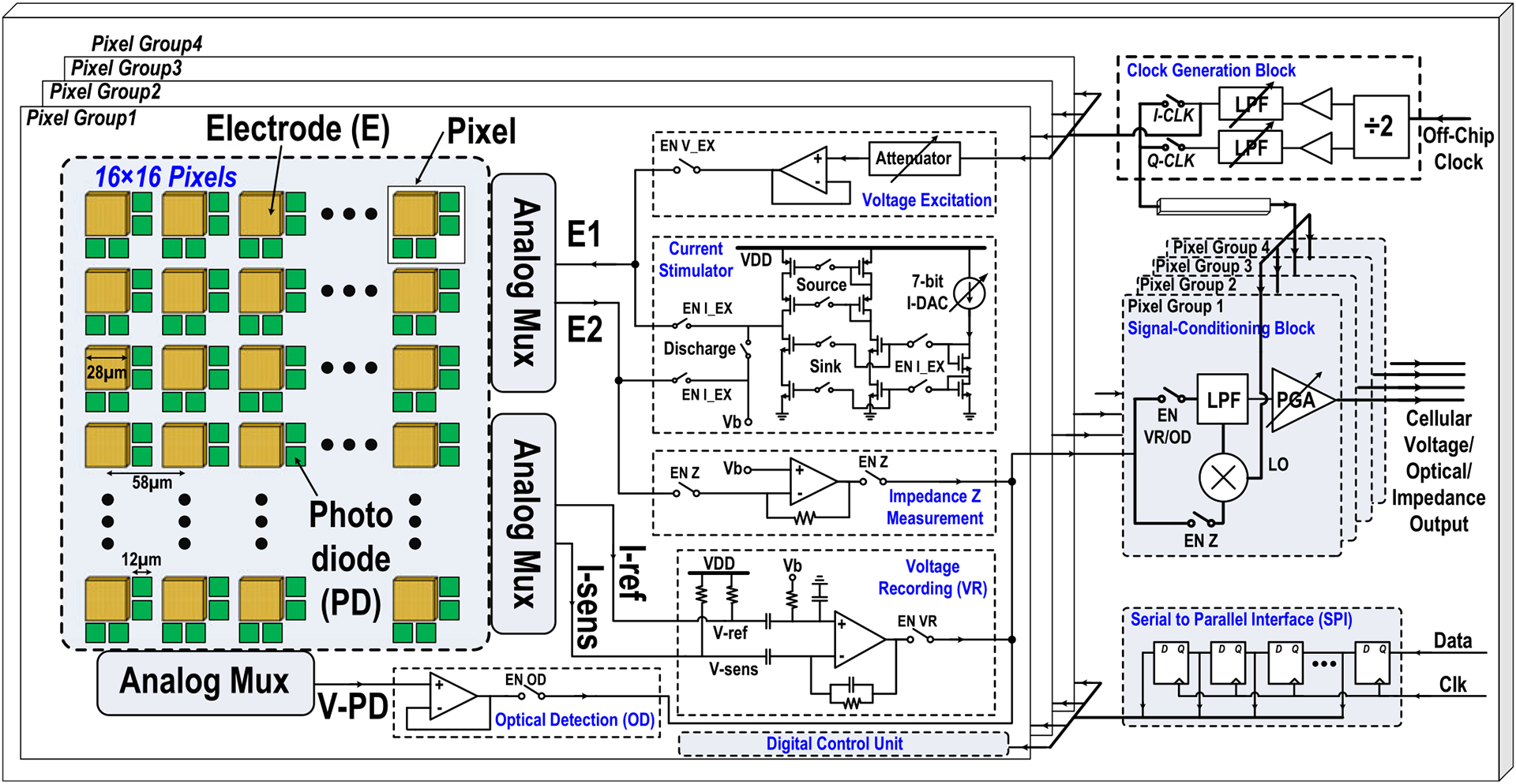
The system-level schematic of the proposed 1024-pixel CMOS multimodality cellular interfacing array.
The in-pixel circuit for extracellular potential recording, complex cellular impedance sensing, and charge-balanced biphasic current stimulation is shown in Fig. 2. It consists of a gold-plated electrode, a series DC blocking capacitor (3.8 pF), a single transistor amplifier (W/L = 20 μm/2 μm), a pseudo resistor (≈400 GΩ), a degeneration resistor (10 kΩ), and reconfiguration switches. Controlled by the switches, the electrode is either directly coupled to the shared circuits in the pixel group for complex impedance sensing and biphasic current stimulation (electrode 1 and electrode 2 in Fig. 2) or ac-coupled to the in-pixel single transistor amplifier for extracellular potential recording (I-sens., I-ref., tail current, and gate bias in Fig. 2). The in-pixel circuit for optical detection is shown in Fig. 3. It includes a reverse-biased p+/nwell/psub photodiode, an NMOS transistor for periodic reset, and a PMOS source follower for readout [43], [44]. Each photodiode is shielded by metal walls (metal and via) to achieve optical isolation.
Fig. 2.
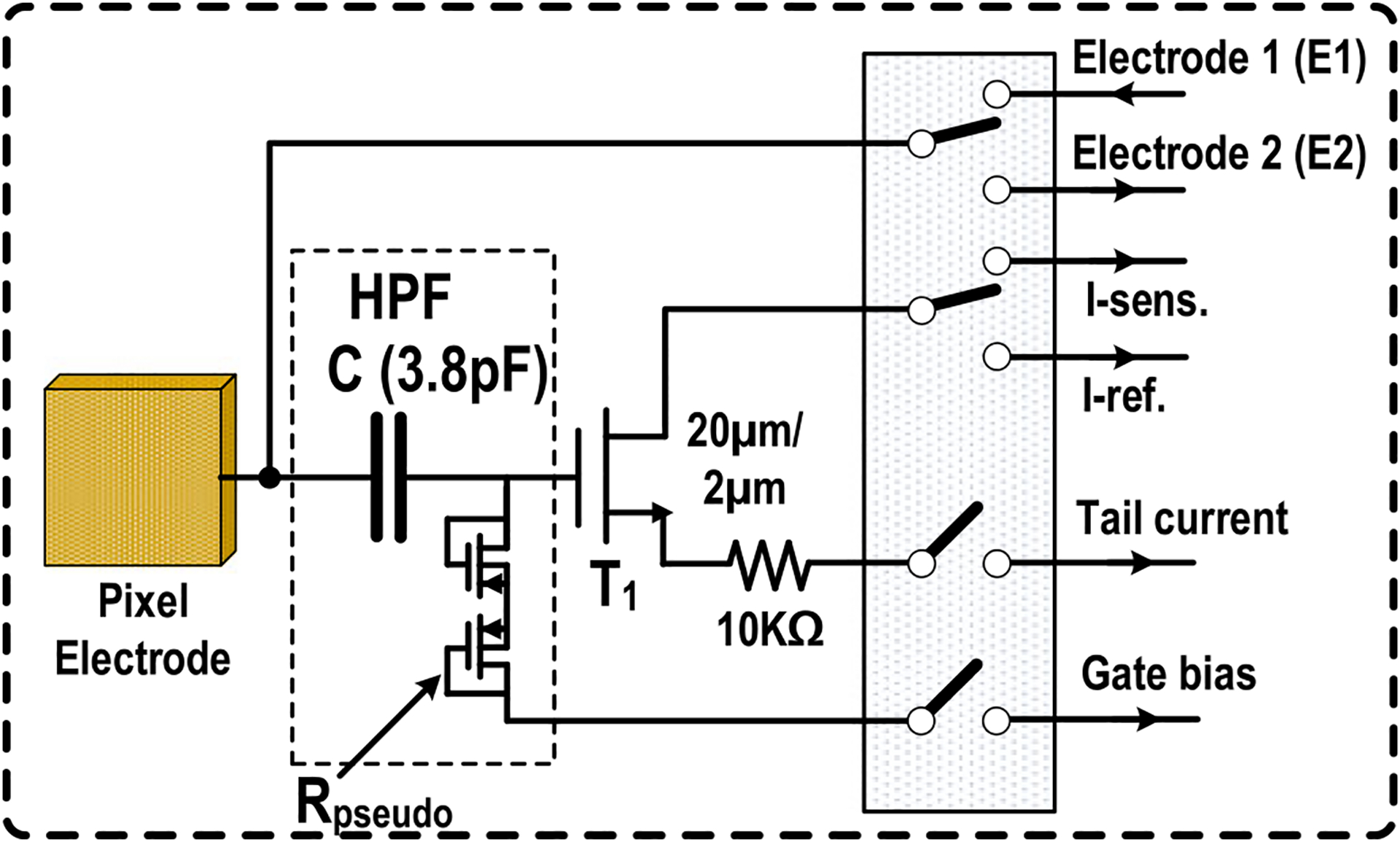
In-pixel circuit for extracellular potential recording, complex impedance sensing, and charge-balanced biphasic current stimulation.
Fig. 3.
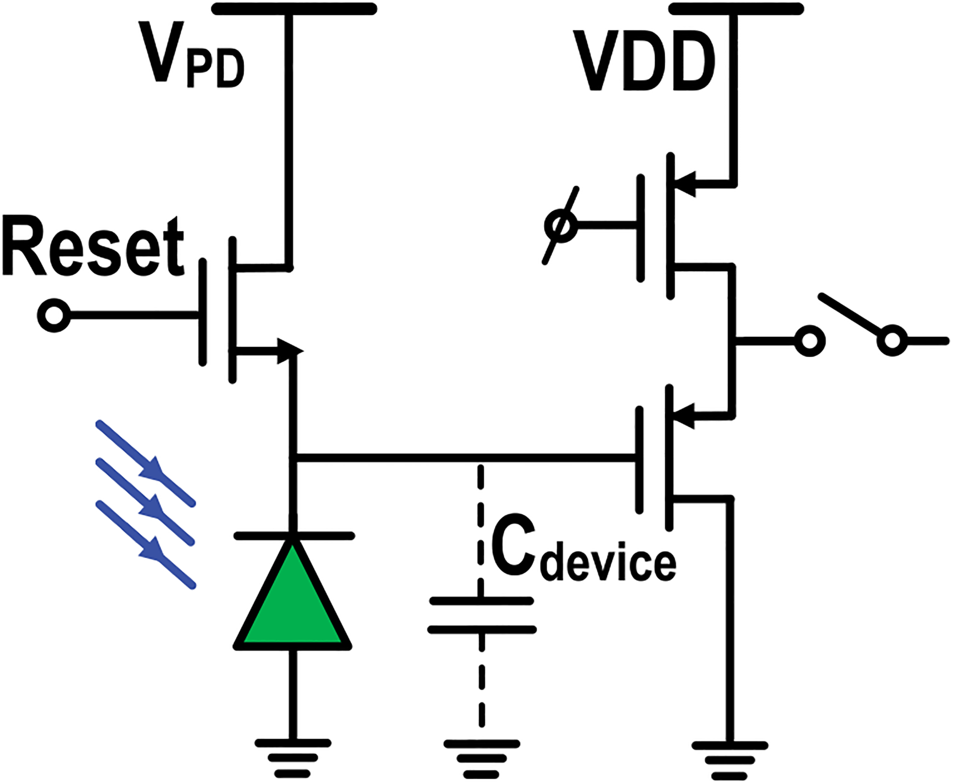
In-pixel circuit for optical detection.
For optical detection, the photodiode cathode is first charged to the photodiode reverse-bias voltage Vpd with a short duration reset pulse. Then, the generated photocurrent discharges the cathode node until the cathode node potential become 0, which is buffered out by the PMOS source follower. Note that the input-referred voltage dynamic range at the cathode node is from Vpd to 0 and each pixel has 4 photodiodes and their corresponding readout circuits.
Next, we will present the circuit details when the pixel group is configured for extracellular potential recording. Fig. 4 shows the circuit schematic in this modality configuration. First, two pixels can be arbitrarily selected from the same pixel group (total 256 pixels) to perform differential cellular potential detection with one pixel for the sensing and the other pixel as the reference. Two in-pixel transistors TR and TS, load resistors RL implemented in pixel group, and 4-bit digitally controlled current source implemented in pixel group are configured as a fully differential amplifier with high-pass response. The voltage gain of the front-end amplifier is programmable from 5 dB-to-14 dB with high-pass lower cut-off frequency of 0.1 Hz, which is sufficient to accurately capture low-frequency local field potential. Compared to the active sensor pixel architecture where a low noise amplifier is implemented in each pixel [43], [44], only one transistor is implemented in each pixel in this design, achieving a substantial pixel size reduction. In addition, compared to the passive sensor pixel architecture [17], the cellular voltage signals are first converted to current signals in pixel by the differential amplifier and then distributed in the current mode; this differential current-mode signaling minimizes the capacitive cross talk among pixels and achieves a fully differential measurement for high common-mode rejection. The detected biopotential signals are further amplified by pixel group low-noise amplifier with 20.3 dB voltage gain. The in-pixel degeneration resistor of 10 kΩ is used to desensitize the mismatches between the sensing pixel transistor TS and the reference pixel transistor TR and between the sensing pseudo resistor and the reference pseudo resistor. The resistor loads RL of 100 kΩ are implemented in each pixel group instead of PMOS loads to minimize flicker noise. The thermal noise generated by the gate bias resistor (pseudo resistor) is filtered out through the double-layer capacitor Cdl at the electrode-electrolyte interface [48] shown in Fig. 4 and the external solution bias electrode. The simulated integrated input-referred noise is 10.5 μVrms for the local field potential band (1-to 300 Hz), 7.7 μVrms for the action potential band (300-to-6000 Hz), and 12.1 μVrms for cardiomyocytes recording (1-to-2000 Hz). The 4-bit digitally controlled tail-current source implemented in pixel group can adjust the tail current between 2.5 μA to 37.5 μA. The voltage gain of the programmable gain amplifier (PGA) in the signal-conditioning block is adjustable from 1.7 dB to 18.0 dB, and therefore the total voltage gain is between 27 dB and 52.3 dB.
Fig. 4.
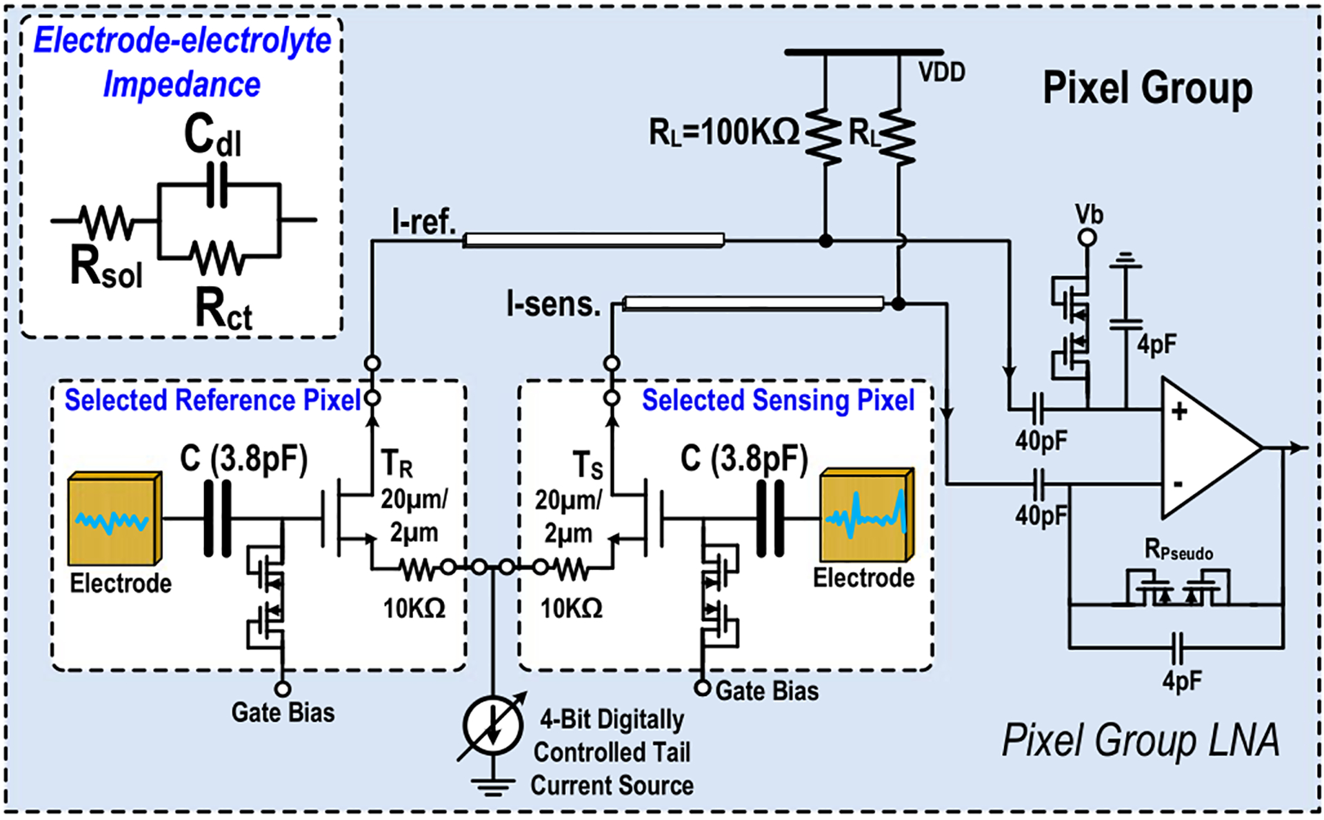
Circuit schematic when two pixels within one pixel group are configured for differential extracellular potential recording.
Fig. 5 shows the circuit schematic when the pixel group is configured for coherent complex impedance sensing. First, two adjacent pixels are selected with one for voltage excitation and the other for current sensing. The two selected in-pixel electrodes (E1 and E2) are DC-coupled and connected to voltage excitation buffer and current sensing TIA, respectively. The operation of coherent complex impedance sensing is as follows. First of all, the fully differential quadrature sinusoidal signals are generated by current-mode logic divide-by-2 circuit and programmable 6th-order low-pass filter. The in-phase signal is fed into the programmable attenuator and then drives the voltage excitation electrode. The resulting cellular current is flowing into the current-sensing pixel electrode, converted to an output voltage signal by TIA, frequency down-converted by the mixer, low-pass filtered, and further amplified by a PGA. The differential quadrature signals are sequentially applied to the mixer local oscillator (LO) port to coherently detect the complex cellular impedance. The simulated total trans-impedance gain for the current sensing chain is 4.6 MΩ, including TIA gain of 129 KΩ, mixer conversion gain of 13 dB, and programmable gain amplifier gain of 18.0 dB. The simulated total output voltage noise divided by the total trans-impedance gain with a mixer LO frequency of 100 kHz and then integrated over a low-pass filter bandwidth of 700 Hz is 54.1 pArms. Since electrodes are DC-coupled, equal DC bias points are critical for reliable impedance sensing and maintaining long-term electrode integrity [48]–[52]. The voltage excitation buffer output DC voltage, culture medium external DC bias voltage, and input DC voltage of the TIA are set to Vb = VDD/2 to minimize undesired faradaic charge transfer [51]. In addition, the sinusoidal voltage excitation amplitude is kept below 50 mV. The minimum impedance sensing time is determined by the programmable low-pass filter RC settling time in the signal-conditioning block after the mixer. With a low-pass filter cut-off frequency of 0.7 kHz, the sinusoidal voltage excitation time is kept less than 4 ms to minimize undesired electrochemical reaction at the electrode-electrolyte interface [51]. The electrode-electrolyte interface impedance can be modeled as solution resistance Rs in series with the double-layer capacitance Cdl in parallel with charge transfer resistance Rct for simplicity [48] shown in Fig. 4. The double-layer capacitance with the electrode size of 30 μm × 30 μm for a gold electrode is between 50 pF~100 pF [52]. Therefore, we choose a relatively high frequency (100 kHz-to-1 MHz) to minimize the artifacts due to electrode-electrolyte interface impedance and achieve precise cellular impedance sensing.
Fig. 5.
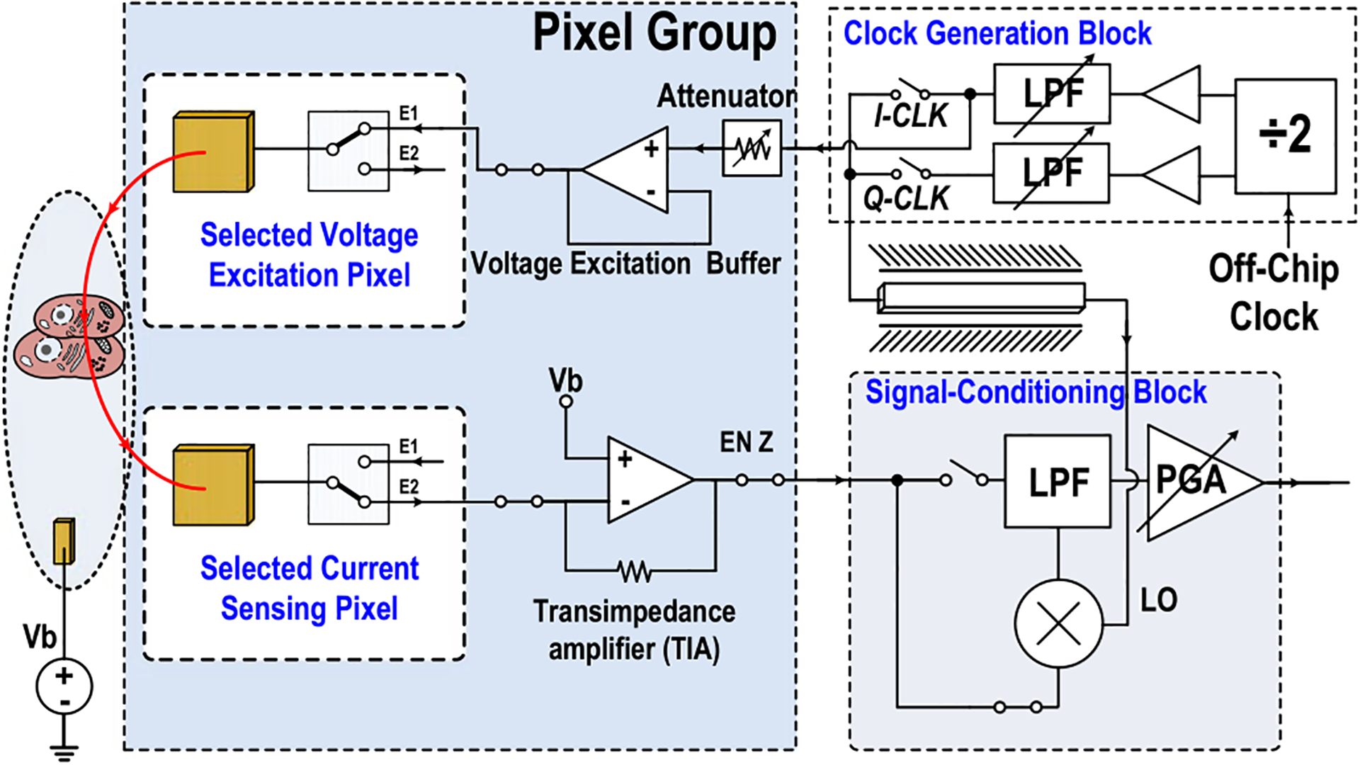
Circuit schematic when the pixel group is configured for coherent complex impedance sensing modality.
The charge-balanced biphasic current stimulation is critical for electrode safety and preventing cell damages, and its related circuits are shown in Fig. 6. Two adjacent pixels are first selected with one for current stimulation and the other for reference/termination. Cathodic current (Scath), anodic current (Sano), and passive charge balancing (Scb) periods are sequentially enabled to complete the biphasic current stimulation and preserve charge balancing for electrode safety [48]–[52]. A 7-bit current digital-to-analog converter (I-DAC) and analog coarse control for I-DAC reference current (I-Ref.) are implemented to cover biphasic current-stimulation range from 100 nA to 32 μA. The current strength, cathodic/anodic pulse width, interphase delay, and inter-pulse interval are fully programmable through SPI.
Fig. 6.
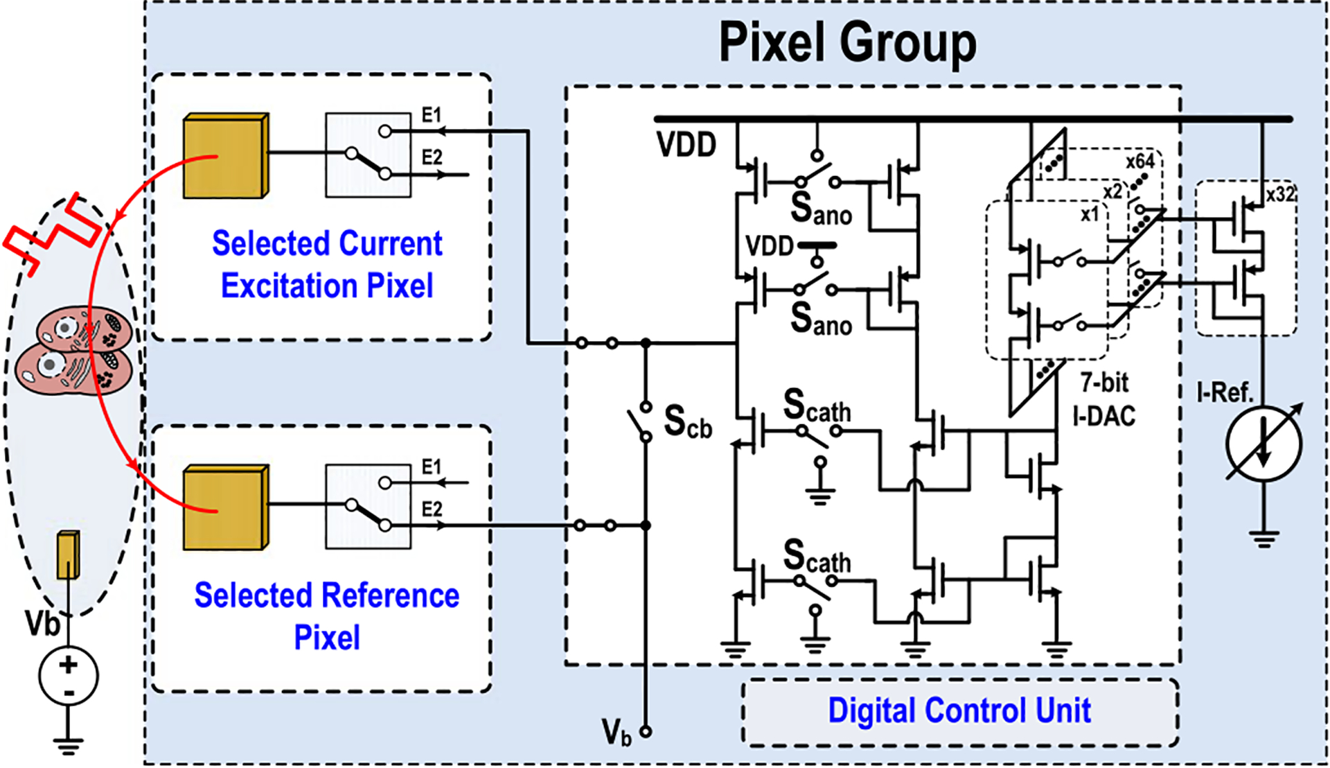
Circuit schematic when the pixel group is configured for the charge-balanced biphasic current stimulation.
III. In-House Biocompatible Packaging
The 1024-pixel CMOS multi-modality cellular interfacing array is fabricated in a standard 130 nm CMOS process with a chip area of 2 mm × 3 mm (Fig. 7). Each pixel occupies 58 μm × 58 μm and contains a 28 μm × 28 μm gold-electrode and four 12 μm × 12 μm photodiodes. Thus, each CMOS array chip achieves 1024 multimodality pixels and 4096 optical sensing sites with a wide FoV of 1.85 mm × 1.85 mm.
Fig. 7.
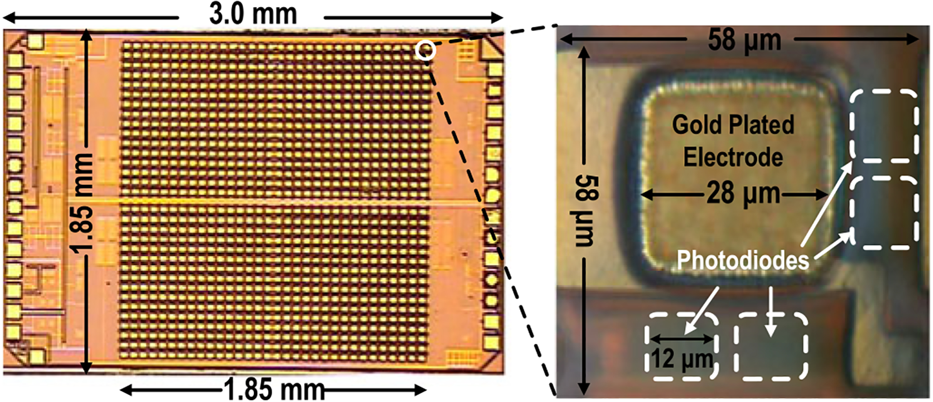
Chip microphotograph.
Since the chip directly interfaces with living cells and corrosive culture medium, biocompatible packaging with high-quality sealing is critical to prevent chip damage and permit the long-term drug effect studies using living cells [53], [54]. Standard CMOS processes, however, mostly use aluminum as the top metal layer and polyimide for the top passivation dielectric layer. To protect the aluminum electrodes in the culture medium, an electro-less gold plating procedure of aluminum-zinc-nickel-gold composite layers is applied to the bare CMOS chips and explained as follows. First, a diced CMOS chip is attached to the glass substrate with black wax for easy handling. The chip is then washed with acetone, methanol, and isopropyl alcohol, and further cleaned with oxygen plasma ions. Next, the diced CMOS chip on the glass substrate is immersed in aluminum etchant (TRANSENE) and then nitric acid to completely remove the aluminum oxide layer on the aluminum metal pads. Finally, the diced chip on the glass substrate is sequentially immersed into off-the-shelf zinc (Zincate, TRANSENE), nickel (Nickelex, TRANSENE), and gold (Immersion gold CF, TRANSENE) solutions following the electro-less gold plating procedure. As the last step, the chip is immersed in an autocatalytic gold solution (AuBEL, UYEMURA) to thicken the gold layer up to 1 μm.
The gold-plated chip is then bonded to the daughter printed-circuit board (PCB) with medical epoxy (302–3M, EPOTEK), and the input/output pads are wire-bonded into the PCB traces. The bonding wires and chip substrate are completely sealed by low shrinkage and high solution-resistance medical epoxy (302–3M, EPOTEK). Since we bias the culture medium to VDD/2 using external reference electrodes and the chip substrate is connected to ground, it is very critical to completely seal the substrate using non-conductive and solution-resistance medical epoxy to avoid undesired electrochemical reaction at the CMOS chip substrate. After the deposited medical epoxy is completely cured, an additional layer of polydimethylsiloxane (PDMS) is applied for improved biocompatibility. Finally, a standard 35 mm cell-culture plate with a laser-cut bottom is mounted on the daughter PCB to hold the culture medium and cell samples (Fig. 8). A separate mother PCB is implemented with level shifters, bypass capacitors, potentiometers, and low drop-out (LDO) regulators to support daughter PCB operations.
Fig. 8.
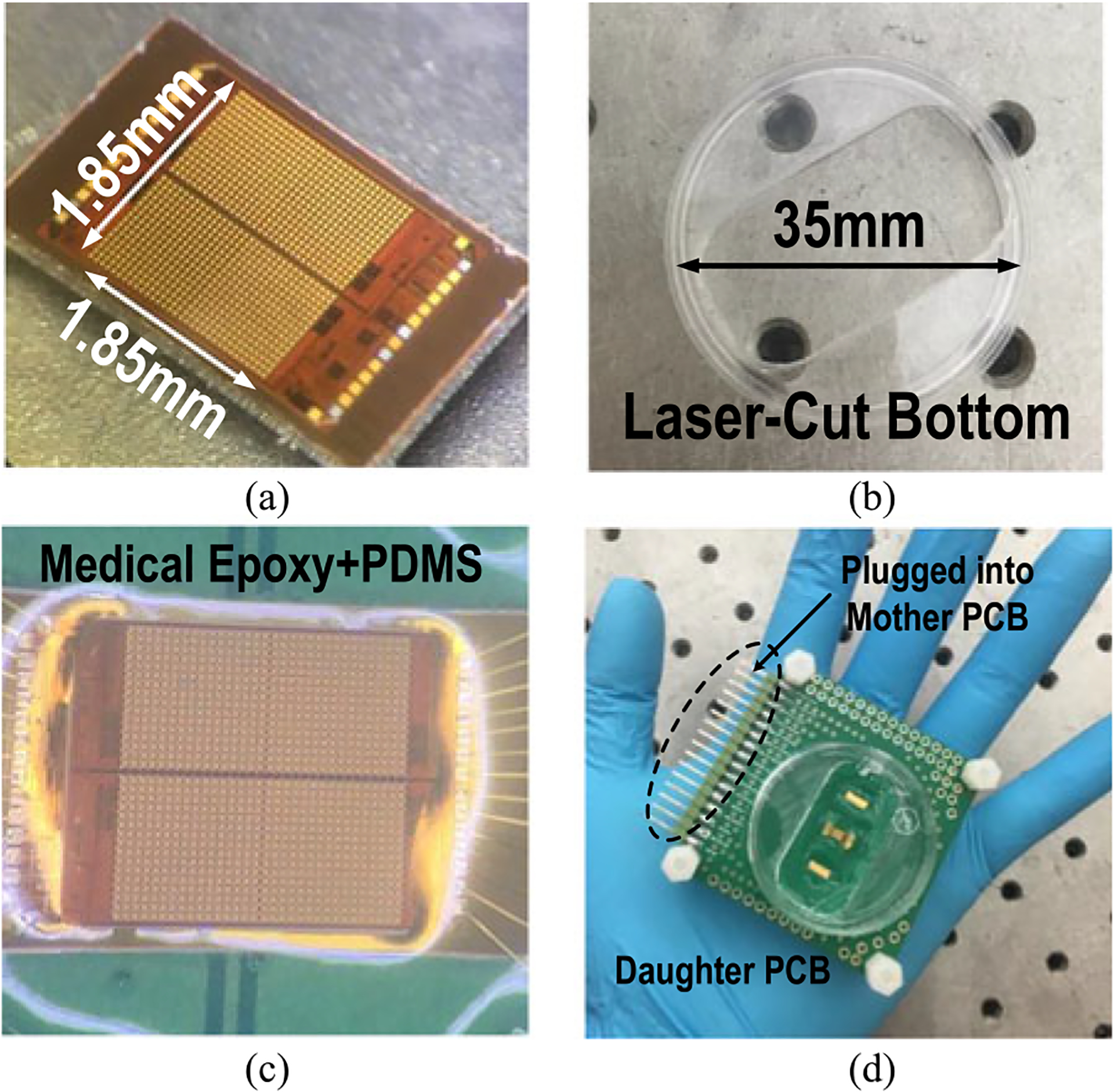
(a) A multimodality cellular interfacing array with gold-plated electrodes. (b) A standard 35-mm cell-culture plate with a laser cut bottom. (c) A biocompatible and robust packaging with a medical epoxy and PDMS. (d) A fully packaged sensor module.
IV. Electrical Measurements
In this section, we will show the electrical measurement results of the proposed 1024-pixel CMOS multimodality cellular interfacing array. The chip is fully packaged in the daughter PCB and plugged into the mother PCB. The FPGA (USB-1616HS, Measurement Computing Corp.) is used to program the CMOS chip through on-chip SPI and readout the chip outputs. D-type batteries are used for power supply to remove 60 Hz noise, and the electrical measurements are performed in a fully shielded chamber.
For the extracellular potential recoding mode, the voltage gain, common-mode rejection ratio (CMRR), and input-referred noise power spectral density (PSD) are measured using the dynamic signal analyzer (Keysight 35670A) with the tail current of 37.5 μA to evaluate the extracellular potential recording functionality (Figs. 9 and 10). The measured average total voltage gain is 52.39 dB with a standard deviation σ of 0.03 dB, measured average CMRR is 67.2 dB with σ of 3.94 dB, and the measured low cut-off frequency is 0.1 Hz. The measured average input-referred noise is 11.7 μVrms integrated from 1 Hz to 300 Hz (local field potential band) with σ = 0.64 μVrms and 7.08 μVrms integrated from 300 Hz to 6 kHz (action potential band) with σ = 0.36 μVrms. In general, to faithfully capture cardiomyocytes action potentials, an analog bandwidth up-to 2 kHz is required. The measured average input-referred noise is 13 μVrms integrated from 1 Hz to 2000 Hz with σ = 0.54 μVrms for cardiomyocytes recording.
Fig. 9.
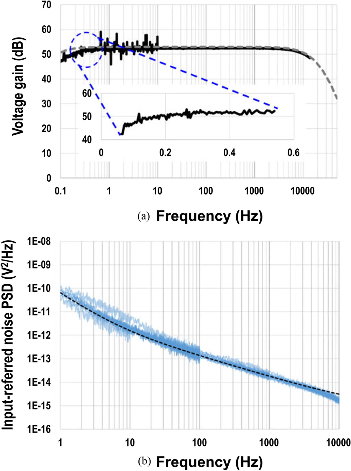
(a) Measured total voltage gain and (b) measured input-referred noise PSD for extracellular potential recording modality.
Fig. 10.
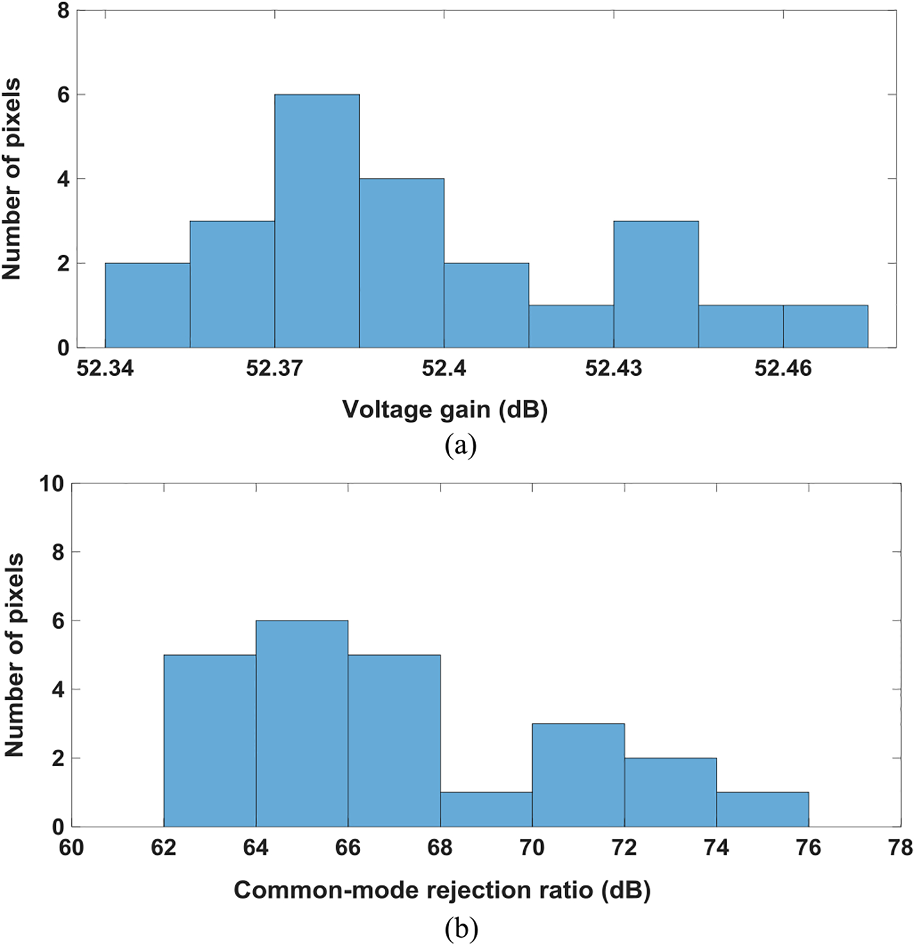
(a) Measured total voltage gain and (b) common-mode rejection ratio (CMRR) histogram.
The integrated input-referred voltage noise is also measured on multiple pixels with different tail current strength of fully differential amplifier in Fig. 4. Fig. 11 shows the histogram of the measured input-referred voltage noise integrated from 300 Hz to 6 kHz (action potential band) on 20 pixels with different tail currents. The total voltage gains with the tail current of 2.5 μA, 10 μA, and 37.5 μA are 45.3 dB, 50.1 dB, and 52.3 dB, respectively. The histogram shows that the integrated input-referred voltage noise variations decrease for larger tail currents. For example, the measured average input-referred integrated noises from 300 Hz to 6 kHz with the tail current of 2.5 μA, 10 μA, and 37.5 μA are 9.94 μVrms, 6.99 μVrms, and 7.08 μVrms with σ = 2.72 μVrms, σ = 0.64 μVrms, and σ = 0.36 μVrms, respectively. This is because the increased tail current of the differential amplifier (Fig. 4) increases the override voltages of sensing pixel and reference pixel transistors TS and TR, and therefore, the differential amplifier is less sensitive to mismatches. For the following cell-based measurements, we use the tail current of 37.5 μA.
Fig. 11.
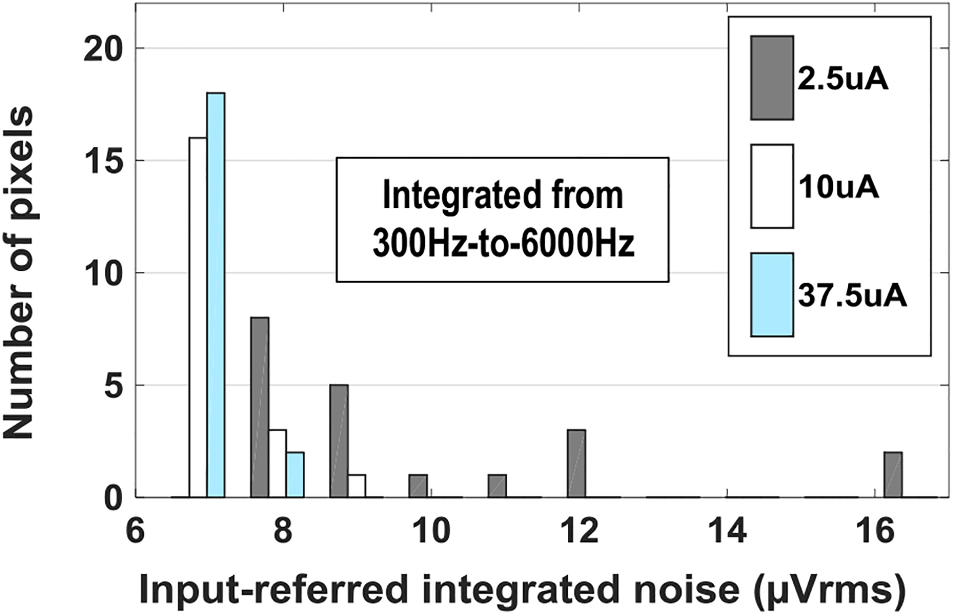
Measured input-referred integrated voltage noise histogram versus different biasing tail current values.
Next, for the cellular optical detection mode, photodiode noise (dark current) with respect to the photodiode reverse-bias voltage VPD is characterized and shown in Fig. 12. We employ the correlated-double-sampling (CDS) scheme to remove the reset noise, offset, fixed pattern noise (FPN), and flicker noise [31], [55] using the FPGA. For photodiode noise characterization, we enable the optical detection modality in the dark room and therefore, the output voltage slope is due to the photodiode dark current integration. Fig. 12 shows the measured output voltage slope decreases as the photodiode reverse-bias voltage Vpd decreases. However, since the input-referred voltage dynamic range for the photocurrent integration is from Vpd to 0 (Fig. 3), the voltage dynamic range decreases as Vpd decreases. Considering the trade-off between the linearity and photodiode dark current, we choose Vpd of 0.8 V for the following cell-based measurements.
Fig. 12.
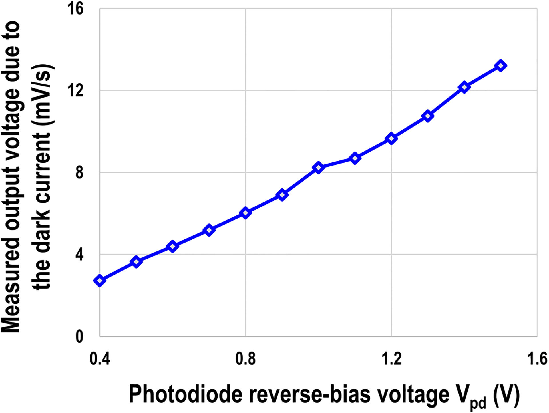
Measured photodiode noise (dark current) versus photodiode reverse-bias voltage VPD.
For the cellular impedance mapping mode, Fig. 13 shows the measured and simulated total output voltage noise power spectral density (PSD) divided by total trans-impedance gain ATotal for the entire current sensing chain, including the TIA, mixer, low-pass filter, and programmable gain amplifier (Fig. 5). The total output voltage noise is measured with TIA input open condition with the mixer LO frequency of 100 kHz and the low-pass filter cut-off frequency of 700 Hz. The measured total output voltage noise is then divided by the total trans-impedance gain ATotal. The measured input-referred current noise integrated over the low-pass filter bandwidth of 700 Hz is 56 pArms, achieving high sensitivity. The low noise current sensing circuit is essential to minimize the amplitude of the voltage excitation signal for electrode safety. Note that the trade-off exists between the measurement speed and the current sensing sensitivity.
Fig. 13.
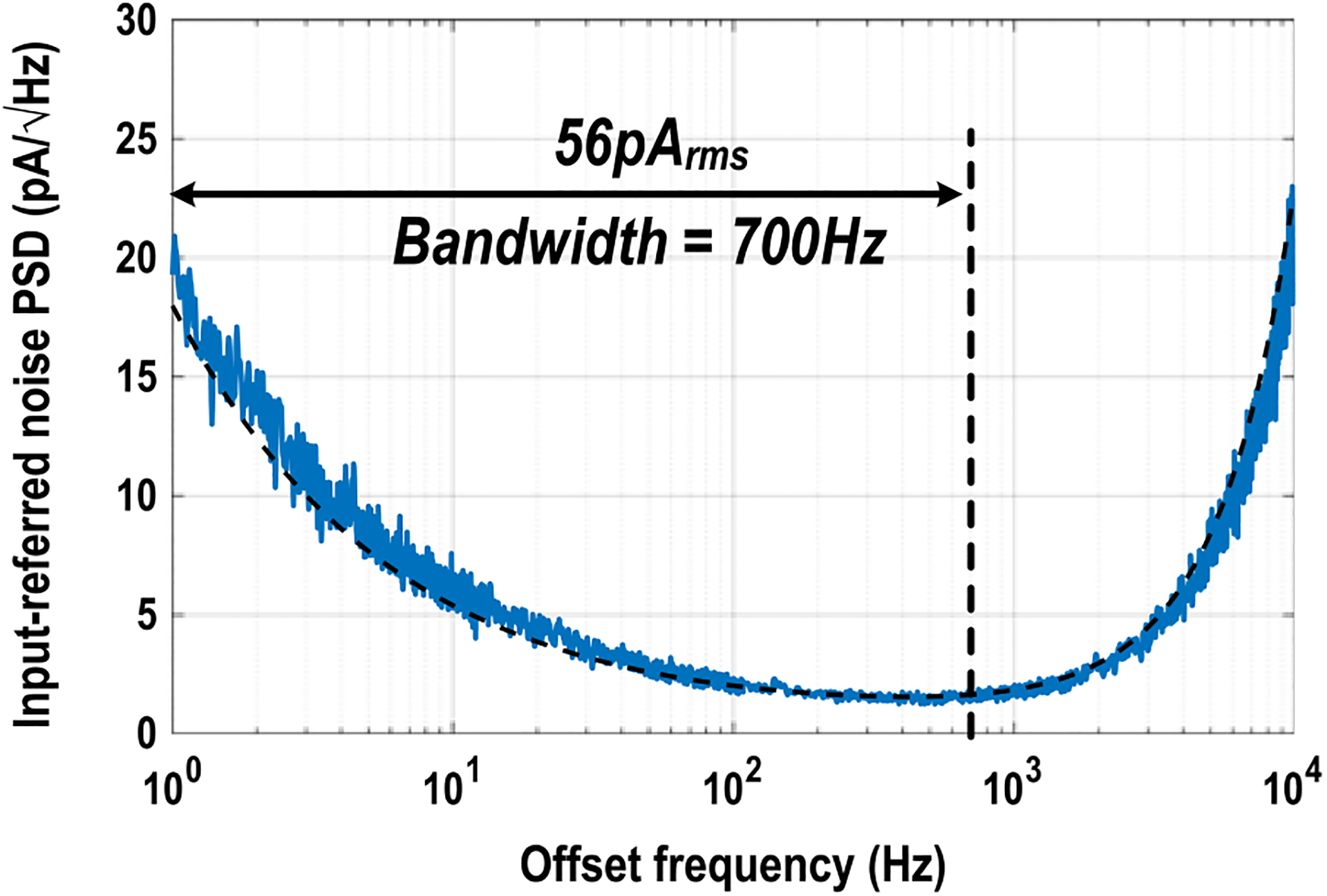
Measured and simulated total output voltage noise power spectral density (PSD) divided by total transimpedance gain ATotal with the mixer frequency of 100 kHz.
The 7-bit biphasic current stimulator is also characterized. Two adjacent pixels are selected with one electrode for current stimulation and the other for reference. Both electrodes are wire-bonded to PCB traces and connected to a load resistor. Fig. 14 shows the measured transient waveform for biphasic current stimulation with the load resistance of 33 kΩ at the pulse frequency of 2 Hz with the stimulation current of 10 μA and pulse width of 0.2 ms. To achieve charge balancing for electrode safety, cathodic current, anodic current, and passive charge balancing (discharge) periods are sequentially applied [56]. The pulse width, frequency, interphase delay, and current strength are fully programmable through the on-chip SPI.
Fig. 14.
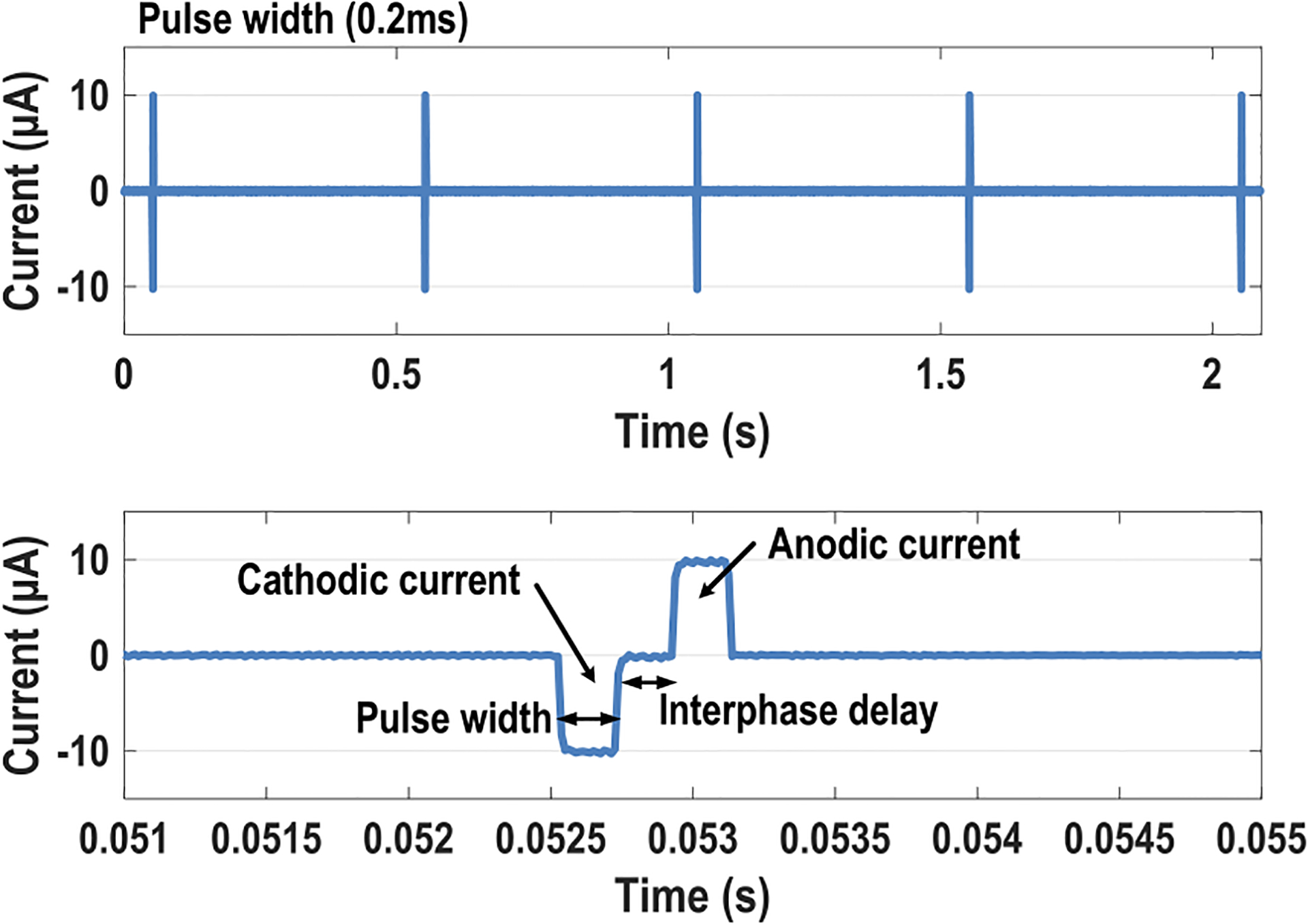
Measured transient waveform for the biphasic current stimulation at the pulse frequency of 2 Hz with the pulsewidth of 0.2 ms, the current of 10 μA, and the load resistor of 33 kΩ.
Next, two electrodes are connected to a load capacitor of 1 nF. Fig. 15 shows the measured cathodic current integration (negative slope) and anodic current integration (positive slope) on the load capacitor of 1 nF with the current amplitude of 970 nA, the pulse width of 0.2 ms, and without the interphase delay. The measured cathodic current integration slope is 975 V/s, which is close to the theoretical slope (970 nA/1 nF = 970 V/s). After anodic current pulse, the residual charges mainly due to the cathodic and anodic current strength and pulse width mismatches are properly discharged by the passive charge balancing period (Scb), achieving the charge balancing. The measured differential nonlinearity (DNL) and integral nonlinearity (INL) of the 7-bit current stimulator are within +0.21/− 0.36LSB and +0.43/−0.52LSB, respectively, shown in Fig. 16.
Fig. 15.

Measured transient waveform for the charge-balanced biphasic current stimulation with the capacitor load of 1 nF, the pulse width of 0.2 ms, and the current amplitude of 970 nA.
Fig. 16.
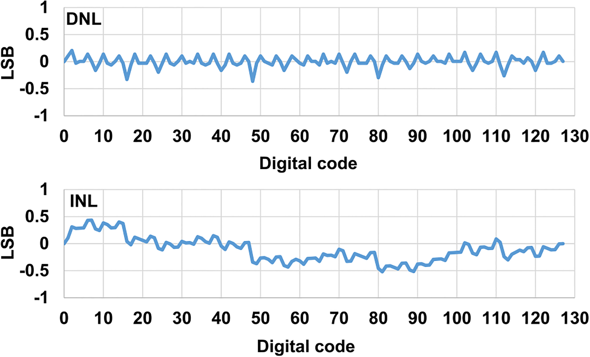
Measured DNL and INL of the 7-bit charge-balanced biphasic current stimulator.
V. On-Chip Cultured Cell-Based Experiments
Neonatal rat ventricular myocytes (NRVMs) were isolated from 1- to 2-day old neonatal rat Sprague-Dawley pups (Charles Rivers) as described previously [57], [58]. Three- fourths of the ventricle was excised and treated with trypsin (Worthington Biochemical Corporation, Freehold, NJ) overnight and then enzymatically treated with collagenase (Worthington Biochemical Corporation, Freehold, NJ). Freshly isolated NRVMs were re-suspended in M199 culture medium (Gibco) supplemented with 10% FBS, glucose, 2 mM GlutaMAX, penicillin, vita-min B12, HEPES buffer, and MEM non-essential amino acids (Gibco). Two 60-minute pre-plating steps were performed to reduce fibroblasts and enrich cardiac myocyte content in the culture. NRVMs were transduced with Ad-GFP day of isolation for 2 hours in suspension at room temperature (RT). Media was changed 24 hours after initial transfection. Spheroids were formed using Aggrewell (STEMCELL, Vancouver, Canada). The Aggrewell 400 plate was sterile as provided from the vendor and was opened in a biosafety cabinet. A total of 0.5 mL of Rinsing Solution (STEMCELL, Vancouver, Canada) was added to each well and the plate was centrifuged for 2 min at 2,000 g. The plate was then incubated for at least 30 minutes at RT or overnight at 4 °C. The plate was washed with PBS prior to use and 0.5 mL of media was added to well and centrifuged for 3 min at 2,000 g. Cell solution containing 1.2 × 10⁶ NRVMs in a 0.5 mL volume was added to each well. Aggrewell plate was centrifuged for 5 min at 200 g. Stereo microscope images are used to verify the cell distribution across the well. The plate was incubated overnight, and its media was replaced by removing 0.5 mL from the plate edge and adding 0.5 mL fresh media. After 3 nights, the spheroids have formed and can be recovered from plate by gently jetting them out with a pipette.
The CMOS chip surface was washed with DPBS (Gibco) and coated with human fibronectin (Corning, Corning NY) at a concentration of 5 μg/mL for 1 hour at 37 °C. Spheroids were added to the CMOS chip surface and allow to adhere overnight. After 24 hours, fresh medium with 10% serum was added. Media is replaced every 2 days (Fig. 19) [59].
Fig. 19.
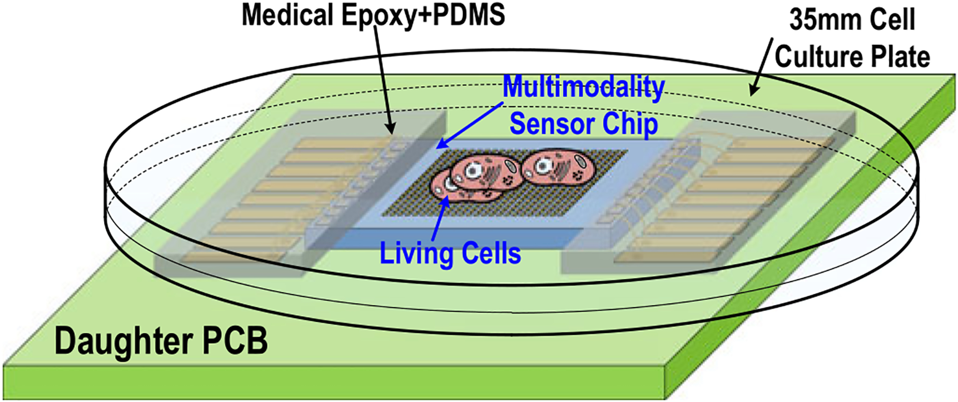
Illustration of in vitro measurement setup with a fully packaged multimodality cellular interfacing array module.
Fig. 17(a) shows the stereo microscope image of the on-chip cultured rat cardiomyocytes. The rat cardiomyocytes are well attached to the CMOS chip surface with successful growth. First of all, the light intensities at 4096 optical detection sites are measured and the measured optical opacity image is shown in Fig. 17(b). The measured optical opacity image closely matches the reference stereo microscope image and clearly shows the 2D distribution of the cultured rat cardiomyocytes on the CMOS chip surface. Furthermore, with the high spatial resolution, Fig. 17(b) also clearly shows the opacity gradient within the rat cardiomyocytes cluster that can be a useful indicator for cell viability tests. For example, in Fig. 17(b), the measured opacity gradient of the rat cardiomyocyte cluster inside the dotted circle using our CMOS chip closely matches that of the reference stereo microscope image. Therefore, the proposed CMOS chip demonstrates in-situ low cost optical detection, particularly useful for massively paralleled fully automated drug screening applications.
Fig. 17.
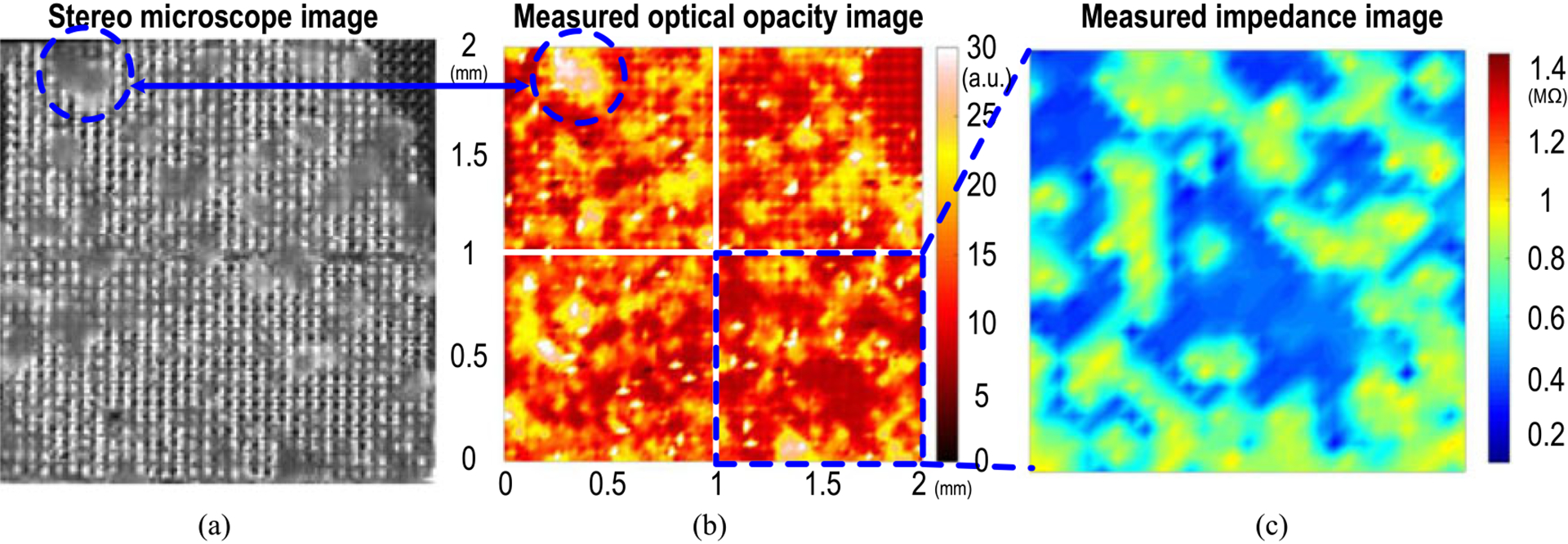
(a) Stereo microscope image, (b) measured optical opacity image, and (c) measured impedance mapping of on-chip cultured rat cardiomyocytes.
Next, impedance sensing is performed on the right lower corner of the chip at 100 kHz in Fig. 17(b). With the spatial resolution of 58 μm, the proposed sensor can measure the impedance of rat cardiomyocyte spheroid/cluster. The measured rat cardiomyocyte spheroid/cluster impedance image is shown in Fig. 17(c) and closely matches the measured optical opacity image in Fig. 17(b) and the reference stereo microscope image in Fig. 17(a). The impedance image shows not only the 2D distribution of the cultured cell clusters on the chip surface but also the cell cluster-to-sensor surface attachment, which is a critical indicator for successful in vitro mammalian cell growth [35]. The cell adhesion is essential to the etiology and pathogenesis of diseases such as inflammatory diseases and oncology [6]. In addition, the cellular impedance is an important cell property parameter that can monitor physiological events such as myocardial ischemia [19] and cardiac muscle contraction [20].
The asynchronous cardiomyocyte spheroids in high concentration are often combined to form a large cardiomyocyte cluster with synchronized beating. Fig. 18(a) and Fig. 18(b) show the reference stereo microscope image and the measured optical opacity image of the on-chip cultured synchronous cardiomyocyte cluster. The measured optical opacity image closely matches the reference stereo microscope image, and the synchronized and autonomous beating is observed under stereo microscope.
Fig. 18.
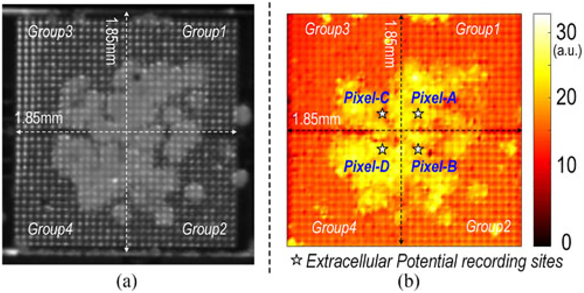
(a) Stereo microscope image and (b) measured optical opacity image of the on-chip cultured synchronous cardiomyocyte cluster.
We also performed extracellular potential recordings for the on-chip cultured rat cardiomyocyte cluster shown in Fig. 18. Fig. 20 shows the measured input-referred extracellular potentials at 4 independent recording sites labeled in Fig. 18(b). The measured extracellular potential recordings achieve high signal-to-noise ratio (SNR) and faithfully capture the fast action potential spikes and slow local field potentials shown in Fig. 20. The measured extracellular potentials at Pixel-A and Pixel-C mostly show fast action potential spikes. On the other hand, the measured extracellular potentials at Pixel-B and Pixel-D clearly show fast action potential spikes together with slow local field potentials. No external filter or signal post-processing is used. The measured action potential spikes at 4 parallel sites are well synchronized, indicating that cardiomyocytes are electrochemically connected. The measured beating rate is 0.34 Hz with a standard deviation of 0.063 Hz. In addition, we directly add 10 μL isoproterenol to the culture medium to test the cell-based drug detection capability of the CMOS multimodality chip. The isoproterenol is a medication used for the treatment of brady-cardia, heart block, and asthma [60]. The measured parallel extracellular potentials are shown in Fig. 21 after the isoproterenol administration. After isoproterenol administration, the cardiomyocytes beating rate increases to 2.38 Hz from 0.34 Hz, and the cardiomyocytes beat more uniformly with a measured standard deviation of 0.007 Hz. Also, the measured action potential spikes at 4 parallel recording sites are well synchronized. Furthermore, the measured input-referred action potential spike amplitude decreases with isoproterenol. The observed cardiomyocytes responses well match the isoproterenol drug effects.
Fig. 20.
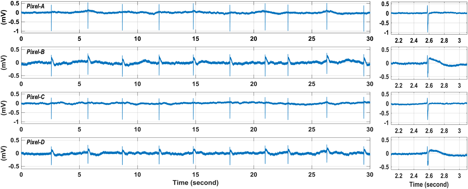
Measured extracellular potentials with on-chip cultured rat cardiomyocytes at four different recording sites in Fig. 18.
Fig. 21.
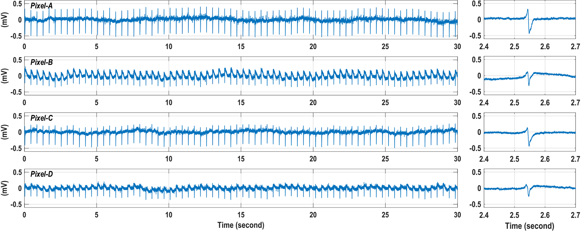
Measured extracellular potential with on-chip cultured rat cardiomyocytes after isoproterenol administration at four parallel recording sites in Fig. 18.
The light transmittance of cardiomyocytes varies with the mechanical movements due to cardiac muscle contraction and relaxation [61]. We measure the real-time light transmittance changes of on-chip cultured rat cardiomyocytes using our CMOS multi-modality chip, which can optically extract the cardiac beating information. For the measurement, we put the CMOS chip module with on-chip cultured rat cardiomyocytes (Fig. 18) in the dark room and illuminate off-the-shelf LED light from the top. Since the incident light intensity is constant, the measured transient light intensity at the optical sensing sites on the CMOS chip shows the transient light transmittance of cardiomyocytes. Note that we perform the measurement using the same cellular sample in Fig. 18, and therefore the optically measured cardiomyocytes beating rate can be directly compared with the measured cardiomyocytes beating rate by extracellular potential recordings (Fig. 21). Fig. 22(a) shows the real-time CMOS chip output voltage for the optical detection with the photodiode reset frequency of 100 Hz, and Fig. 22(b) shows the measured transient light intensity extracted using correlated double sampling of the output voltage slope. To faithfully capture the cardiac muscle mechanical movements, we use the optical sampling frequency (photodiode reset frequency) of 100 Hz for a temporal resolution of 10 ms [61]. The measured transient light intensity in Fig. 22(b) clearly shows the cyclic patterns of systolic and diastolic rhythms for on-chip cultured rat cardiomyocytes. Fig. 23 shows the measured real-time light intensities at 4 parallel recording sites labeled in Fig. 18, recorded concurrently. The larger light intensity changes are observed at Pixel-B indicating stronger cardiac muscle contraction around that pixel compared to the other pixels. The real-time light intensities also show that the cardiac muscle contractions are well synchronized, which is consistent with the measured extracellular potential recording (Fig. 21). The optically measured cardiomyocytes beating rate is 2.59 Hz with the standard deviation of 0.08 Hz, closely aligned with the extracellular potential recording results. The real-time light intensity at a pixel without cardiomyocytes is also measured as a control experiment and plotted together with the real-time light intensity at Pixel-B in Fig. 23, showing high SNR and confidence level of the cardiomyocytes light intensity measurements. Although we do not enable two sensing modalities simultaneously for each pixel, with fully integrated on-chip high-speed electronics, the multiple sensing modalities are multiplexed with sufficiently small time interval to achieve multi-modal sensing on the same on-chip cellular samples with biological relevance.
Fig. 22.
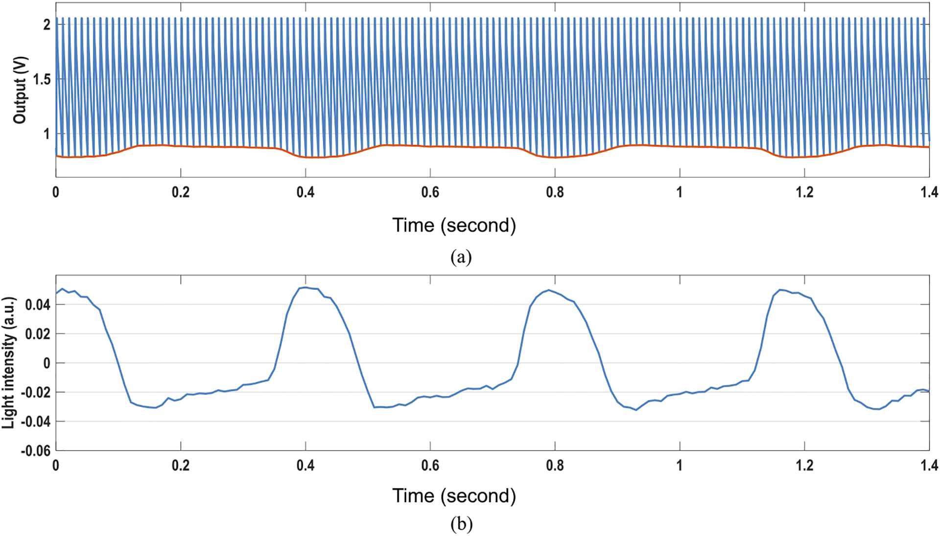
Measured transient (a) chip output voltage slope for optical detection and transient (b) light intensity.
Fig. 23.
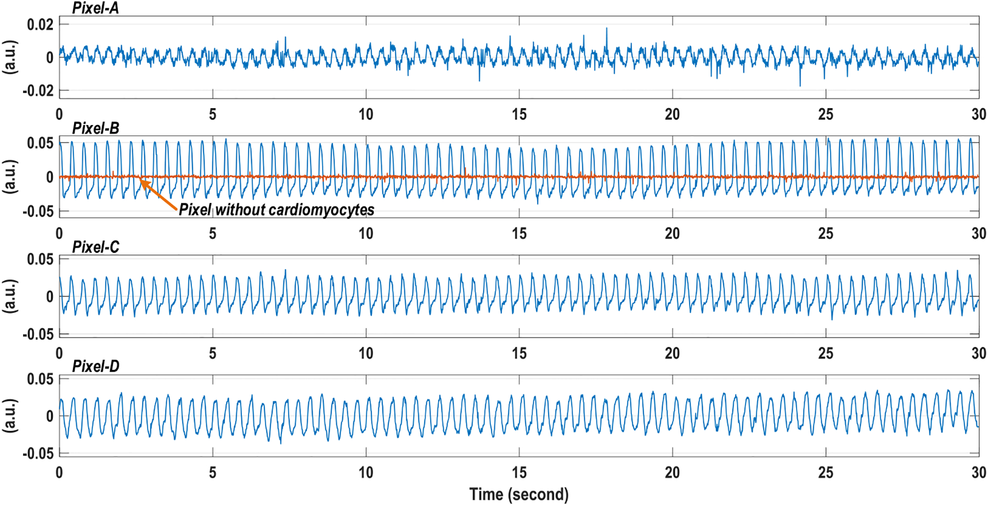
Measured transient light intensities at four parallel recording sites in Fig. 18. A pixel without cardiomyocytes is also recorded as the control experiment.
The cell pacing experiments with the on-chip cultured rat cardiomyocytes are also performed. The fluorescent-microscope image of the on-chip cultured rat cardiomyocytes is shown in Fig. 24. The rat cardiomyocyte spheroids achieve full confluency and very slow synchronized autonomous beating is observed (1 beat/min). For cell pacing experiments, the rat cardiomyocyte spheroids are first stimulated at 4 independent sites (Fig. 24) with the pulse frequency of 1 Hz, the pulse width of 200 μs, and the current amplitude of 33 μA. Then, we gradually increase the pulse width from 200 μs to 4 ms to measure the pacing threshold while keeping the pulse frequency and the current amplitude same. At the same time, the extracellular potential recordings are enabled at 4 independent sites (Fig. 24) to monitor the stimulation response of the on-chip cultured rat cardiomyocytes. Note that since the stimulation artifact could saturate the potential recording amplifier, simultaneous stimulation and potential recording on the same location are challenging [62], [63]. Therefore, the extracellular potential recordings are enabled on the recording sites which are 656 μm apart from the biphasic current stimulation sites (Fig. 24) to allow response time delay.
Fig. 24.
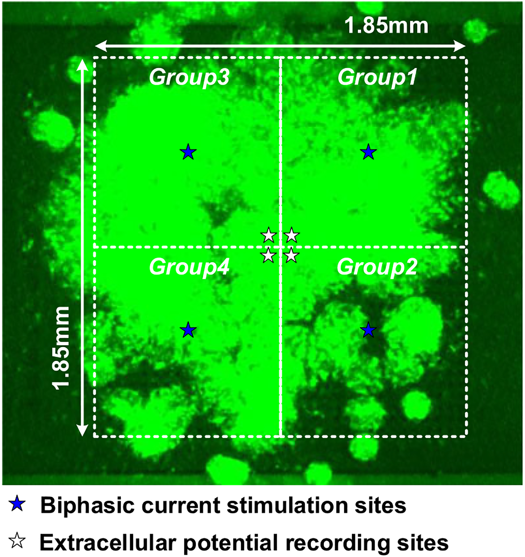
The fluorescent-microscope image of the on-chip cultured rat cardiomyocytes.
The overlay plot of the measured extracellular potentials at the pixel group1 (Fig. 24) with the biphasic current stimulations is shown in Fig. 25. The measurement results show that the on-chip cultured rat cardiomyocyte spheroids are successfully paced with the pulse width greater than 2 ms and the measured capture rate is 100% with the pulse width greater than 2 ms. The output referred evoked action potential spike amplitude is 538 mV, which is corresponding to the input referred voltage amplitude of 1.34 mV. It also shows that the time delay between the current stimulations and evoked action potential spikes, the amplitude of the spikes, and the shape of the spikes are consistent for 10 continuous biphasic current stimulations.
Fig. 25.
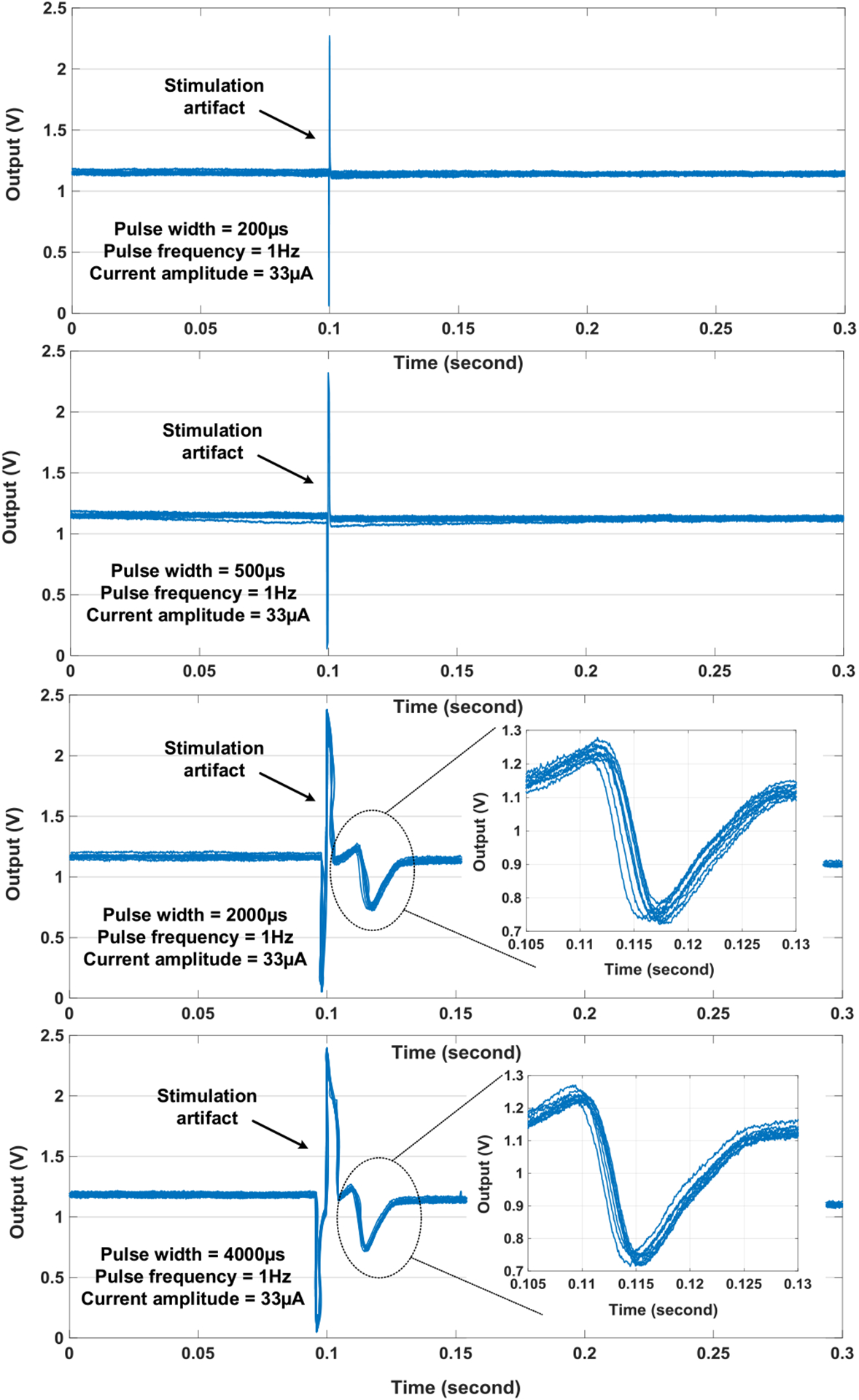
The overlay plot of the measured extracellular potential recordings at the pixel group 1 with the on-chip biphasic current stimulation versus different biphasic current stimulation pulse width.
VI. Conclusion
In this paper, we present a 1024-pixel CMOS multimodality cellular interfacing array chip for holistic cell characterization and cell-based drug screening applications. Each pixel can be independently configured to perform extracellular potential recording, cellular impedance sensing, optical detection, and biphasic current stimulation. Each pixel size is 58 μm × 58 μm including a 28 μm × 28 μm gold-plated electrode and four 12 μm × 12 μm photodiodes. We also present our in-house biocompatible packaging with robust solution resistance and demonstrate successful culturing of rat cardiomyocytes on the CMOS chip. The measured optical opacity image of on-chip cultured rat cardiomyocytes achieves high spatial resolution and closely matches the reference stereo microscope image. The measured extracellular potentials achieve high SNR and accurately capture the isoproterenol drug effects. Furthermore, real-time optical measurement of cardiomyocyte beating is demonstrated to record the transient cardiac muscle contraction and relaxation events and measure the cardiac beating rate, which aligns well with extracellular potential recording. The on-chip cultured rat cardiomyocytes are successfully paced with the on-chip biphasic current stimulator, and the pacing threshold and capture rate are also measured. The cell-based measurement results demonstrate the utility and benefit of the proposed CMOS multimodality cellular interfacing array system for fully automated and massively paralleled drug screening and new drug development in the pharmaceutical industry (Table I). The proposed concept of multi-modality sensing may also benefit other biomedical sensing platforms [65]–[70].
TABLE I.
Comparison Table of State-of-the-Art Silicon-Based Biosensors
| Modality | Pixel Size (μm2) | Number of Pixels | Field of View (mm2) | On-Chip Cell Assay | Measured Cellular Phenotype | Tech (nm) | |
|---|---|---|---|---|---|---|---|
| This work | Potential Recording, Impedance Sensing, Optical Detection, Current Stimulation | 58 × 58 | 1024 | 1.85 × 1.85 | Rat CMs | Extracellular Potential, Impedance/Optical Imaging, Cardiac Muscle Contraction/Relaxation, Stimulation | CMOS 130 |
| [11] | Magnetic Movement Tracking | 180 × 180 | 64 | 1.2 × 1.2 | Cardiac Progenitors | Cardiac Muscle Contraction/Relaxation | CMOS 65 |
| [16] | Potential Recording | 7.5 × 7.5 | 16k | 1 × 1 | Snail Neurons | Extracellular Potential | CMOS 500 |
| [17] | Potential Recording, Current Stimulation | 17.5 × 17.5 | 26k | 3.85 × 2.1 | Rat Cortical Neurons | Extracellular Potential | CMOS 350 |
| [18] | Impedance Sensing | 90 × 90 | 100 | 1 × 1 | DNA, Protein | DNA Hybridization, Protein Detection | CMOS 350 |
| [21] | PH Sensing | 10.2 × 10.2 | 65k | 2.87 × 2.87 | Hexokinase, Glucose | Glucose Concentration | CMOS 350 |
| [22] | Optical Detection, PH Sensing | 10 × 10 | 4096 | 0.64 × 0.64 | 45 μm Microbeads | N.A | CMOS 180 |
| [29] | Fluorescence | 250 × 250 | 56 | 3 × 3 | DNA Molecule | DNA Hybridization | CMOS 350 |
| [43] | Potential Recording, Impedance Sensing, Optical Detection | 80 × 100 | 144 | 1.5 × 1.68 | CMs, Neurons, Cancer | Extracellular Potential, Impedance/Optical Imaging, Bioluminescent | CMOS 130 |
| [64] | Potential Recording, Impedance Sensing, Stimulation, Neurotransmitter Detection | 13.5 × 1.35 | 59,760 | 4.48 × 2.43 | Rat Cortical Neurons | Extracellular Potential, Stimulation | CMOS 180 |
Acknowledgment
The authors would like to thank Dr. Todd McDevitt and Dr. Tracy Hookway of Gladstone/UCSF, Dr. Mark Styczynski and Amy Su of Georgia Tech, and the members of Georgia Tech GEMS lab for technical discussions.
This work was in part sponsored by the Semiconductor Research Corporation under task 2484.001 and National Science Foundation under Award 1454555 and Award 1610677. This work was supported by the National Science Foundation Graduate Research Fellowship Program under Grant DGE-1148903. Any opinions, findings, and conclusions or recommendations expressed in this material are those of the author(s) and do not necessarily reflect the views of the National Science Foundation. This paper was recommended by Associate Editor G. Yuan.
Biographies

Jong Seok Park (S’13) received the B.S. degree in electrical and electronic engineering (highest honors) from Yonsei University, Seoul, South Korea, in 2012. He is currently working toward the Ph.D. degree in electrical and computer engineering with Georgia Institute of Technology, Atlanta, GA, USA. His current research interests include novel electromagnetic structure, RF and millimeter-wave circuits, and sensors for biomedical applications.
Mr. Park received a study-abroad scholarship from the Korea Foundation for Advanced Studies in 2012. He was also the recipient of the Analog Device Inc. Outstanding Student Designer Award in 2014, the co-recipient of the RFIC Best Student Paper Award (first Place) in 2014, the recipient of the IEEE Custom Integrated Circuits Conference Best Student Paper Award in 2015, the recipient of the Sensors Conference Best Live Demo Award (second place) in 2016, and the recipient of the SSCS Predoctoral Achievement Award for 2016–2017.

Moez Karim Aziz (S’16) received the B.S.E. degree in bioengineering (summa cum laude) and the B.A. degree in biophysics with distinction (summa cum laude) from the University of Pennsylvania, Philadelphia, PA, USA. He is currently a National Science Foundation Graduate Research Fellow completing the M.S. and Ph.D. degrees in electrical and computer engineering under Prof. H. Wang with Georgia Institute of Technology, Atlanta, GA, USA.
Mr. Aziz received the Herman P. Schwan Award in Bioengineering at the University of Pennsylvania as an undergraduate student and the Georgia Tech Presidential Fellowship as a graduate student. He is also a co-recipient of the IEEE Sensors Best Live Demo Award (second place) for the paper “Live Demonstration: A 1024-Pixel CMOS Multi-Modality Sensing Array for Cell-Based Assays.” He is a member of Tau Beta Pi and Phi Beta Kappa.

Sensen Li (S’16) received the B.Eng. and B.A. degrees from Zhejiang University, Hangzhou, China, in 2013. He is currently working toward the Ph.D. degree in electrical engineering with Georgia Institute of Technology, Atlanta, GA, USA. His current research interests include millimeter-wave integrated circuits and packaging, antenna, and electronics codesign.

Taiyun Chi (S’11) received the B.S.(Hons.) degree from the University of Science and Technology of Chin, Hefei, China, in 2012. He is currently working toward the Ph.D. degree in electrical engineering with Georgia Institute of Technology, Atlanta, GA, USA. His current research interests include RF/millimeter-wave/terahertz integrated circuits and integrated biomedical sensors and actuators.
Mr. Chi received the Microwave Theory and Techniques Society (MTT-S) Graduate Fellowship for Medical Applications in 2016, the Analog Devices Inc. Outstanding Student Designer Award in 2015, the Texas Instruments IEEE Custom Integrated Circuits Conference Student Scholarship Award in 2014, the Georgia Tech GEDC Fellowship in 2012, and the USTC Guo Moruo Presidential Scholarship in 2012. He was also a co-recipient of the IEEE Sensors Best Live Demo Award (second place) in 2016, and the IEEE Radio Frequency Integrated Circuits Symposium Best Student Paper Award (second place) in 2016.

Sandra Ivonne Grijalva received the B.S. degree in biomedical engineering from the University of Arizona, Tucson, AZ, USA, in 2014. She is currently working toward the Ph.D. degree in biomedical engineering from the joint program between Georgia Institute of Technology and Emory University, Atlanta, GA, USA. Her current research interests include creating 2-D and 3-D models of the sinoatrial node (pacemaker) in the heart to understand source-sink mismatch.
Ms. Grijalva has received the Ford Foundation Fellowship, the NRSA NIH F31 Fellowship, the Alfred P. Sloan Foundation Fellowship, the Goizueta Foundation Fellowship, and the GT Presidential Fellowship to fund her doctoral research.

Jung Hoon Sung received the M.D. degree from Yonsei University College of Medicine, Wonju, South Korea, in 1998, and the Ph.D. degree in neuroimmunopharmacology from Korea University College of Medicine, Seoul, South Korea, in 2006. He was a Visiting Professor with the Department of Biomedical Engineering, Emory University and Georgia Institute of Technology, Atlanta, GA, USA, in 2015. He is currently an Associate Professor in electrophysiology with the Department of Cardiology, CHA Bundang Medical Center, CHA University, Seoul. His current research interests include biological pacemaker and sinus node function for biomedical applications.

Hee Cheol Cho received the Ph.D. degree in the field of cardiac electrophysiology from the University of Toronto, Toronto, ON, Canada, in 2003. He received postdoctoral fellowship training at Johns Hopkins Medical Institution in the Division of Cardiology. During his fellowship at Johns Hopkins from 2003 to 2006, he has pioneered the concept of biological pacemakers as alternatives to electronic cardiac pacemaker devices. This led to an investment of $1M/year for three years from Medtronic, Inc., to form a venture biotech company in Baltimore, MD, USA, where he was the Director of the R&D program. In 2009, he resumed his academic career at Cedars-Sinai Medical Center, Los Angeles, CA, USA, and at University of California, Los Angeles, as an Assistant Professor. There, he made breakthrough discovery that a single-gene transfer sufficed to create biological pacing in a small and large animal models. In 2014, he joined Emory University, Atlanta, GA, USA, and substantially expanded his research group to advance the concept of biological pacemakers toward clinical reality. He and his team are working with Emory Hospital’s cardiologists to validate long-term biological pacing in a clinically relevant porcine model of complete heart block.

Hua Wang (M’05-SM’15) received the M.S. and Ph.D. degrees in electrical engineering from California Institute of Technology, Pasadena, CA, USA, in 2007 and 2009, respectively. He worked at Intel Corporation and Skyworks Solutions. He joined the School of Electrical and Computer Engineering (ECE), Georgia Institute of Technology, Atlanta, GA, USA, as an Assistant Professor in 2012. His research interests include innovating mixed-signal, RF, and millimeter-wave integrated circuits and hybrid systems for wireless communication, radar, imaging, and bioelectronics applications.
Dr. Wang received the National Science Foundation CAREER Award in 2015, the IEEE MTT-S Outstanding Young Engineer Award in 2017, the Georgia Tech Sigma Xi Young Faculty Award in 2016, the DURIP Award in 2014, the Georgia Tech ECE Outstanding Junior Faculty Member Award in 2015, and the Lockheed Dean’s Excellence in Teaching Award in 2015. He currently holds the Demetrius T. Paris Junior Professorship of the School of ECE at Georgia Tech. His research group Georgia Tech Electronics and Micro-System (GEMS) Lab has received multiple best paper awards, including the IEEE RFIC Best Student Paper Awards in 2014 (first place) and 2016 (second place), the IEEE Custom Integrated Circuits Conference (CICC) Best Student Paper Awards in 2015, the 2016 IEEE Microwave Magazine Best Paper Award, the 2016 IEEE SENSORS Best Live Demo Award (second place), as well as multiple best paper award finalists at IEEE conferences. He is an Associate Editor of the IEEE Microwave and Wireless Components Letters. He is a Technical Program Committee Member for the IEEE International Solid-State Circuits Conference, the IEEE Radio Frequency Integrated Circuits Symposium (RFIC), the IEEE CICC, and the IEEE Biopolar/BiCMOS Circuits and Technology Meeting. He is a Steering Committee Member for IEEE RFIC and IEEE CICC. He serves as the Chair of the Atlanta’s IEEE Circuits and Systems Society/IEEE Solid-State Circuits Society (SSCS) joint chapter, which received the IEEE SSCS Outstanding Chapter Award in 2014.
Contributor Information
Sandra Ivonne Grijalva, Department of Biomedical Engineering, Emory University, Atlanta, GA 30322 USA.
Jung Hoon Sung, CHA Bundang Medical Center, CHA University, Seoul 135-081, South Korea.
Hee Cheol Cho, Department of Biomedical Engineering, Emory University, Atlanta, GA 30322 USA.
Hua Wang, School of Electrical and Computer Engineering, Georgia Institute of Technology, Atlanta, GA 30332 USA.
References
- [1].Lee H, Liu Y, Westervelt R, and Ham D, “IC/Microfluidic hybrid system for magnetic manipulation of biological cells,” IEEE J. Solid-State Circuits, vol. 41, no. 6, pp. 1471–1480, Jun. 2006. [Google Scholar]
- [2].Tunuguntla R et al. , “Bioelectronic light-gated transistors with biologically tunable performance,” Adv. Mater, vol. 27, pp. 831–836, Nov. 2014. [DOI] [PubMed] [Google Scholar]
- [3].Jenkner M, Tartagni M, Hierlemann A, and Thewes R, “Cell-based CMOS sensor and actuator array,” IEEE J. Solid-State Circuits, vol. 39, no. 12, pp. 2431–2437, Dec. 2004. [Google Scholar]
- [4].Iniewski K, Integrated Microsystems: Electronics, Photonics, and Biotechnology. Boca Raton, FL, USA: CRC Press, 2012. [Google Scholar]
- [5].Wang H, “Integrated biosensors in CMOS,” in Proc. 54th IEEE Int. Midwest Symp. Circuits Syst, Aug. 2011, pp. 1–4. [Google Scholar]
- [6].Shamah S and Cunningham B, “Label-free cell-based assays using photonic crystal optical biosensors,” Analyst, vol. 136, pp. 1090–1102, Jan. 2011. [DOI] [PubMed] [Google Scholar]
- [7].Wang H, “Magnetic sensors for diagnostic medicine: CMOS-based magnetic particle detectors for medical diagnosis applications,” IEEE Microw. Mag, vol. 14, no. 5, pp. 110–130, Jul-Aug 2013. [Google Scholar]
- [8].Wilke R et al. , “Identifying generic risk factors for serious adverse drug reactions: Current progress and challenges,” Nature Rev. Drug Discovery, vol. 6, no. 11, pp. 904–916, Nov. 2007. [DOI] [PMC free article] [PubMed] [Google Scholar]
- [9].Shah R, “Cardiac repolarization and drug regulation,” Drug Safety, vol. 30, no. 12, pp. 1093–1110, Dec. 2007. [DOI] [PubMed] [Google Scholar]
- [10].Esch E, Bahinski A, and Huh D, “Organs-on-chips at the frontiers of drug discovery,” Nature Rev. Drug Discovery, vol. 14, no. 4, pp. 248–260, Apr. 2015. [DOI] [PMC free article] [PubMed] [Google Scholar]
- [11].Wang H, Mohdavi A, Tirrell D, and Hajimiri A, “A magnetic cell-based sensor,” Lab Chip, vol. 12, pp. 4465–4471, 2012. [DOI] [PubMed] [Google Scholar]
- [12].Banerjee P and Bhunia AK, “Mammalian cell-based biosensors for pathogens and toxins,” Trends Biotechnol, vol. 27, no. 3, pp. 179–188, Mar. 2009. [DOI] [PubMed] [Google Scholar]
- [13].Gil G, Mitchell R, Chang S, and Gu M, “A biosensor for the detection of gas toxicity using a recombinant bioluminescent bacterium,” Biosens. Bioelectron, vol. 15, nos. 1/2, pp. 23–30, Mar. 2000. [DOI] [PubMed] [Google Scholar]
- [14].Kubisch R, Bohrn U, Fleischer M, and Stutz E, “Cell-based sensor system using L6 cells for broad band continuous pollutant monitoring in aquatic environments,” Sensors, vol. 12, pp. 3370–3393, Mar. 2012. [DOI] [PMC free article] [PubMed] [Google Scholar]
- [15].Harrison RR and Charles C, “A low-power low-noise CMOS amplifier for neural recording applications,” IEEE J. Solid-State Circuits, vol. 38, no. 6, pp. 958–965, Jun. 2003. [Google Scholar]
- [16].Eversmann B et al. , “A 128 × 128 CMOS biosensor array for extracellular recording of neural activity,” IEEE J. Solid-State Circuits, vol. 38, no. 12, pp. 2306–2317, Dec. 2003. [Google Scholar]
- [17].Ballini M et al. , “A 1024-channel CMOS microelectrode array with 26,400 electrodes for recording and stimulation of electrogenic cells in vitro,” IEEE J. Solid-State Circuits, vol. 49, no. 11, pp. 2705–2719, Nov. 2014. [DOI] [PMC free article] [PubMed] [Google Scholar]
- [18].Manickam A, Chevalier A, McDermont M, Ellington A, and Hassibi A, “A CMOS electrochemical impedance spectroscopy (EIS) biosensor array,” IEEE Trans. Biomed. Circuits Syst, vol. 4, no. 6, pp. 379–390, Dec. 2010. [DOI] [PubMed] [Google Scholar]
- [19].Yufera A, Rueda A, Munoz J, Doldan R, Leger G, and Rodriguez-Villegas E, “A tissue impedance measurement chip for myocardial ischemia detection,” IEEE Trans. Circuits Syst. I, Reg. Papers, vol. 52, no. 12, pp. 2620–2628, Dec. 2005. [Google Scholar]
- [20].Schmid Y, Burgel S, Misun P, Hierlemann A, and Frey O, “Electrical impedance spectroscopy for microtissue spheroid analysis in hanging-drop networks,” ACS Sens, vol. 1 no. 8, pp. 1028–1035, Jul. 2016. [DOI] [PMC free article] [PubMed] [Google Scholar]
- [21].Cheah B et al. , “An integrated circuit for chip-based analysis of enzyme kinetics and metabolite quantification,” IEEE Trans. Biomed. Circuits Syst, vol. 10, no. 3, pp. 721–730, Jun. 2016. [DOI] [PubMed] [Google Scholar]
- [22].Huang X, Yu H, Liu X, Jiang Y, Yan M, and Wu D, “A dual-mode large-array CMOS ISFET sensor for accurate and high-throughput pH sensing in biomedical diagnosis,” IEEE Trans. Biomed. Eng, vol. 62, no. 9, pp. 2224–2233, Sep. 2015. [DOI] [PubMed] [Google Scholar]
- [23].Lee I et al. , “A reconfigurable and portable highly sensitive biosensor platform for ISFET and enzyme-based sensors,” IEEE Sens. J, vol. 16, no. 11, pp. 4443–4451, Jun. 2016. [Google Scholar]
- [24].Wang H, Chen Y, Hassibi A, Scherer A, and Hajimiri A, “A frequency-shift CMOS magnetic biosensor array with single-bead sensitivity and no external magnet,” in Proc. IEEE Int. Solid-State Circuits Conf., Feb. 2009, pp. 438–439. [Google Scholar]
- [25].Wang H, Sideris C, and Hajimiri A, “A frequency-shift based CMOS magnetic biosensor with spatially uniform sensor transducer gain,” in Proc. IEEE Custom Integr. Circuits Conf., Sep. 2010, pp. 1–4. [Google Scholar]
- [26].Liu PP et al. , “Magnetic relaxation detector for microbead labels,” IEEE J. Solid-State Circuits, vol. 47, no. 4, pp. 1056–1064, Apr. 2012. [DOI] [PMC free article] [PubMed] [Google Scholar]
- [27].Wang H, Weng C, and Hajimiri A, “Phase noise and fundamental sensitivity of oscillator-based reactance sensors,” IEEE Trans. Microw. Theory Techn, vol. 61, no. 5, pp. 2215–2229, May 2013. [Google Scholar]
- [28].Pai A, Khachaturian A, Chapman S, Hu A, Wang H, and Hajimiri A, “A handheld magnetic sensing platform for antigen and nucleic acid detection,” Analyst, vol. 139, no. 6, pp. 1403–1411, Dec. 2013. [DOI] [PubMed] [Google Scholar]
- [29].Jang B, Cao P, Chevalier A, Ellington A, and Hassibi A, “A CMOS fluorescent-based biosensor microarray,” in Proc. IEEE Int. Solid-State Circuits Conf., 2009, pp. 436–437. [Google Scholar]
- [30].Patounakis G, Shepard KL, and Levicky R, “Active CMOS array sensor for time-resolved fluorescence detection,” IEEE J. Solid-State Circuits, vol. 41, no. 11, pp. 2521–2530, Nov. 2006. [DOI] [PMC free article] [PubMed] [Google Scholar]
- [31].Eltoukhy H, Salama K, and Gamal A, “A 0.18-μm CMOS bioluminescence detection lab-on-chip,” IEEE J. Solid-State Circuits, vol. 41, no. 3, pp. 651–662, Mar. 2006. [Google Scholar]
- [32].Manaresi N et al. , “A CMOS chip for individual cell manipulation and detection,” IEEE J. Solid-State Circuits, vol. 38, no. 12, pp. 2297–2305, Dec. 2003. [Google Scholar]
- [33].Lee H, Kwon K, Li W, and Ghovanloo M, “A power-efficient switched-capacitor stimulating system for electrical/optical deep brain stimulation,” IEEE J. Solid-State Circuits, vol. 50, no. 1, pp. 360–374, Jan. 2015. [Google Scholar]
- [34].Christen J and Andreou A, “Design, fabrication, and testing of a hybrid CMOS/PDMS microsystem for cell culture and incubation,” IEEE Trans. Biomed. Circuits Syst, vol. 1, no. 1, pp. 3–18, Mar. 2007. [DOI] [PubMed] [Google Scholar]
- [35].Feng Y, Mitchison T, Bender A, Young D, and Tallarico J, “Multi-parameter phenotypic profiling: Using cellular effects to characterize small-molecule compounds,” Nature Rev. Drug Discovery, vol. 8, pp. 567–578, Jul. 2009. [DOI] [PubMed] [Google Scholar]
- [36].Stefano P et al. , “Monophasic and biphasic electrical stimulation induces a precardiac differentiation in progenitor cells isolated from human heart,” Stem Cells Develop, vol. 23, no. 8, pp. 888–898, Dec. 2013. [DOI] [PMC free article] [PubMed] [Google Scholar]
- [37].Chan Y et al. , “Electrical stimulation promotes maturation of cardiomyocytes derived from human embryonic stem cells,” J. Cardiovascular Transl. Res, vol. 6, no. 6, pp. 989–999, Dec. 2013. [DOI] [PubMed] [Google Scholar]
- [38].Davidovics N, Fridman G, Chiang B, and Santina C, “Effects of biphasic current pulse frequency, amplitude, duration, and interphase gap on eye movement responses to prosthetic electrical stimulation of the vestibular nerve,” IEEE Trans. Neural Syst. Rehabil. Eng, vol. 19, no. 1, pp. 84–94, Feb. 2011. [DOI] [PMC free article] [PubMed] [Google Scholar]
- [39].Wong J, Olson J, Morhart M, and Chan K, “Electrical stimulation enhances sensory recovery; a randomized controlled trial,” Ann. Neurol, vol. 77, no. 6, pp. 996–1006, May 2015. [DOI] [PubMed] [Google Scholar]
- [40].Heck CN et al. , “Two-year seizure reduction in adults with medically intractable partial onset epilepsy treated with responsive neurostimulation: Final results of the RNS system pivotal trial,” Epilepsia, vol. 55, no. 3, pp. 432–441, 2014. [DOI] [PMC free article] [PubMed] [Google Scholar]
- [41].Kringelbach ML, Jenkinson N, Owen SLF, and Aziz TZ, “Translational principles of deep brain stimulation,” Nature Rev. Neurosci, vol. 8, no. 8, pp. 623–635, 2007. [DOI] [PubMed] [Google Scholar]
- [42].Berényi A, Belluscio M, Mao D, and Buzsáki G, “Closed-loop control of epilepsy by transcranial electrical stimulation,” Science, vol. 337, no. 6095, pp. 735–737, Aug. 2012. [DOI] [PMC free article] [PubMed] [Google Scholar]
- [43].Park J, Chi T, Butts J, Hookway T, McDevitt T, and Wang H, “A multimodality CMOS sensor array for cell-based assay and drug screening,” in Proc. IEEE Int. Solid-State Circuits Conf., Feb. 2015, pp. 208–209. [DOI] [PubMed] [Google Scholar]
- [44].Chi T et al. , “A multi-modality CMOS sensor array for cell-based assay and drug screening,” IEEE Trans. Biomed. Circuits Syst, vol. 9, no. 6, pp. 801–814, Dec. 2015. [DOI] [PubMed] [Google Scholar]
- [45].Park J et al. , “Live demonstration; A multi-modality CMOS sensor array for cell-based assay and drug screening,” in Proc. IEEE Biomed. Circuits Syst. Conf., Oct. 2015, p. 1. [DOI] [PubMed] [Google Scholar]
- [46].Park J et al. , “A high-density CMOS multi-modality joint sensor/stimulator array with 1024 pixels for holistic real-time cellular characterization,” in Proc. IEEE Symp. VLSI Circuits, Jun. 2016, pp. 1–2. [Google Scholar]
- [47].Park J et al. , “Live demonstration: A 1024-pixel CMOS multi-modality sensing array for cell-based assays,” in Proc. IEEE Sens, Oct. 2016, p. 1. [Google Scholar]
- [48].Franks W, Schenker I, Schmutz P, and Hierlemann A, “Impedance characterization and modeling of electrodes for biomedical applications,” IEEE Trans. Biomed. Eng, vol. 52, no. 7, pp. 1295–1302, Jul. 2005. [DOI] [PubMed] [Google Scholar]
- [49].Weiland J, Anderson D, and Humayun M, “In vitro electrical properties for iridium oxide versus titanium nitride stimulating electrodes,” IEEE Trans. Biomed. Eng, vol. 49, no. 12, pp. 1574–1579, Dec. 2002. [DOI] [PubMed] [Google Scholar]
- [50].Aryan N, Kaim H, and Rothermel A, Stimulation and Recording Electrodes for Neural Prostheses. New York, NY, USA: Springer, 2015. [Google Scholar]
- [51].Merrill D, Bikson M, and Jefferys J, “Electrical stimulation of excitable tissue: Design of efficacious and safe protocols,” J. Neurosci. Methods, vol. 141, no. 2, pp. 171–198, Feb. 2005. [DOI] [PubMed] [Google Scholar]
- [52].Moulton S, Barisci J, Bath A, Stella R, and Wallace G, “Studies of double layer capacitance and electron transfer at a gold electrode exposed to protein solutions,” Electrochimica Acta, vol. 49, no. 24, pp. 4223–4230, Sep. 2004. [Google Scholar]
- [53].Zia M et al. , “A microfabricated electronic microplate platform for low-cost repeatable biosensing applications,” in Proc. IEEE Int. Electron Devices Meeting, Dec. 2015, pp. 29.4.1–29.4.4. [Google Scholar]
- [54].Zia M et al. , “3-D integrated electronic microplate platform for low-cost repeatable biosensing applications,” IEEE Trans. Compon., Packag., Manuf. Technol, vol. 6, no. 12, pp. 1827–1833, Dec. 2016. [Google Scholar]
- [55].Wang H, Kosai S, Sideris C, and Hajimiri A, “An ultrasensitive CMOS magnetic biosensor array with correlated double counting noise suppression,” in Proc. IEEE Int. Microw. Symp, May 2010, pp. 616–619. [Google Scholar]
- [56].Thurgood B, Warren D, Ledbetter N, Clark G, and Harrison R, “A wireless integrated circuit for 100-channel charge-balanced neural stimulation,” IEEE Trans. Biomed. Circuits Syst, vol. 3, no. 6, pp. 405–414, Dec. 2009. [DOI] [PubMed] [Google Scholar]
- [57].Kapoor N, Liang W, Marbán E, and Cho H, “Direct conversion of quiescent cardiomyocytes to pacemaker cells by expression of Tbx18,” Nature Biotechnol. vol. 31, pp. 54–62, Jan. 2013. [DOI] [PMC free article] [PubMed] [Google Scholar]
- [58].Kapoor N, Galang G, Marbin E, and Cho H, “Transcriptional suppression of connexin43 by TBX18 undermines cell-cell electrical coupling in postnatal cardiomyocytes,” J. Biol. Chem, vol. 286, no. 16, pp. 14073–14079, Apr. 2011. [DOI] [PMC free article] [PubMed] [Google Scholar]
- [59].Wang H et al. , “Cell culture and cell based sensor on CMOS,” in Proc. IEEE Biomed. Circuits Syst. Conf., Oct. 2014, pp. 1–4. [Google Scholar]
- [60].Shen H, Illustrated Pharmacology Memory Cards: PharMnemonics, 1st ed. Minireview, Twinsburg, Ohio, 2007. [Google Scholar]
- [61].Hossain MM et al. , “Non-invasive characterization of mouse embryonic stem cell derived cardiomyocytes based on the intensity variation in digital beating video,” Analyst, vol. 135, pp. 1624–1630, Jun. 2010. [DOI] [PubMed] [Google Scholar]
- [62].Dura B, Chen M, Inan O, Kovacs G, and Giovangrandi L, “High-frequency electrical stimulation of cardiac cells and application to artifact reduction,” IEEE Trans. Biomed. Circuits Syst, vol. 59, no. 5, pp. 1381–1390, May 2012. [DOI] [PubMed] [Google Scholar]
- [63].Mendrela A et al. , “A bidirectional neural interface circuit with active stimulation artifact cancellation and cross-channel common-mode noise suppression,” IEEE J. Solid-State Circuits, vol. 51, no. 4, pp. 955–965, Apr. 2016. [Google Scholar]
- [64].Dragas J et al. , “In vitro multi-functional microelectrode array featuring 59 760 electrodes, 2048 electrophysiology channels, stimulation, impedance measurement, and neurotransmitter detection channels,” IEEE J. Solid-State Circuits, vol. 52, no. 6, pp. 1576–1590, Jun. 2017. [DOI] [PMC free article] [PubMed] [Google Scholar]
- [65].Zhu C, Zhang L, Geng J, Shi X, and Qian H, “A micro-array bio detection system based on a GMR sensor with 50-ppm sensitivity,” Sci. China Inf. Sci, vol. 60, Aug. 2017, Art. no. 082403. [Google Scholar]
- [66].Zhou X, Huang C, and Hall D, “Giant magnetoresistive biosensor array for detecting magnetorelaxation,” IEEE Trans. Biomed. Circuits Syst, vol. 11, no. 4, pp. 755–764, Aug. 2017. [DOI] [PubMed] [Google Scholar]
- [67].Geng J, Zhang L, Zhu C, and Qian H, “An oscillator-based CMOS magneto-sensitive biosensor with in-situ switched capacitor calibration scheme,” IEEE Microw. Wireless Compon. Lett, vol. 26, no. 8, pp. 640–642, Aug. 2016. [Google Scholar]
- [68].Zhang L, Yu Z, and He X, “Design and implementation of ultralow current-mode amplifier for biosensor applications,” IEEE Trans. Circuits Syst. II, Exp. Briefs, vol. 56, no. 7, pp. 540–544, Jul. 2009. [Google Scholar]
- [69].Zhang L, He X, Wang Y, and Yu Z, “A fully integrated CMOS nanoscale biosensor microarray,” IEEE Custom Integrated Circuits Conf., Sep. 2011. [Google Scholar]
- [70].Evander M, Ricco A, Morser J, Kovacs G, Leung L, and Giovangrandi L, ”Microfluidic impedance cytometer for platelet analysis,” Lap Chip, 2013, 13, 722–729. [DOI] [PubMed] [Google Scholar]


